Application Note 01/2007 IonScan 800 – Ultra ... - Roth & Rau AG
Application Note 01/2007 IonScan 800 – Ultra ... - Roth & Rau AG
Application Note 01/2007 IonScan 800 – Ultra ... - Roth & Rau AG

Create successful ePaper yourself
Turn your PDF publications into a flip-book with our unique Google optimized e-Paper software.
<strong>Roth</strong> & <strong>Rau</strong> <strong>AG</strong>, Gewerbering 3, 09337 Hohenstein-Ernstthal, Germany<br />
source along the surface normal and to control the etching<br />
distance. An axis system for such applications should have 2<br />
tilt and 3 linear axes.<br />
2. <strong>IonScan</strong> <strong>800</strong> system layout<br />
The <strong>IonScan</strong> <strong>800</strong> system is designed for wafer based film<br />
thickness trimming in semiconductor technology. With the<br />
handler and the process module, it is possible to create a<br />
cluster layout of the entire system, which is able to integrate<br />
both two load-locks and up to three process modules<br />
(Fig. 2).<br />
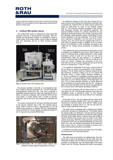
Process<br />
Chamber<br />
Ion Beam<br />
Chamber<br />
Fig. 2: General view of the <strong>IonScan</strong> <strong>800</strong><br />
Handler with<br />
Load-Lock<br />
The process chamber is fed with a 4 port handling robot<br />
(Fig. 2 right) by Brooks Automation Inc. or ASYS Automatisierungssysteme<br />
GmbH & Co. KG. The robot comprises a<br />
separately pumped load-lock, fitted with cassette lift and indexer,<br />
as well as a prealigner with combined OCR and barcode<br />
reader. A cluster system with a number of process<br />
chambers can be set up by any residual port allocation desired.<br />
The system components for ion beam trimming are housed<br />
in the process chamber (Fig. 2 left). The chamber size is<br />
about 0.80 m x 0.80 m x 0.50 m. Approximately 5 x 10 -5 Pa<br />
residual gas pressure is feasible with the turbomolecular<br />
pump set (2300 l/s). All door flanges are fitted with double V i-<br />
ton O-rings and are pumped differentially.<br />
Impedane<br />
Matching<br />
Discharge<br />
Arrangement<br />
Neutraliser<br />
Z Axis<br />
Fig. 3: Filament-free RF ion beam source cyberis 40-i<br />
(Shields to protect against redeposition removed.)<br />
An additional chamber at the front door houses the ion<br />
beam source to be accessed for maintenance activities upon<br />
a separate lid. A filament-free ion beam source cyberis 40-i<br />
made by <strong>Roth</strong> & <strong>Rau</strong> is used in the <strong>IonScan</strong> system<br />
(Fig. 3) 6 . The source is mounted completely in the vacuum<br />
with discharge chamber and impedance matching. The<br />
plasma excitation consists of a primary cylindrical coil supporting<br />
the discharge housing in the middle. According to the<br />
ICP principle, radio frequency power (13.65 MHz) is transferred<br />
inductively to the gas discharge. The full RF impedance<br />
matching is integrated in the rear part of the source<br />
housing. Thus, the source may be supplied with a 50 Ω coaxial<br />
cable of arbitrary length. In addition to the ion beam<br />
source, a hot filament or a RF neutraliser are used to neutralise<br />
the ion charge during processing of isolating substrates.<br />
Three different focussing multi-aperture grid systems made<br />
of graphite are available for the source. Each system consists<br />
of 3 individual grids of different geometry, which enable<br />
intentional control of both the ion flow and the focus<br />
characteristics. With the grid systems, it is possible to<br />
achieve a maximal total ion flow to 100 mA, as well as up to<br />
2 keV ion energy. Typically, the processes on the Ion-<br />
Scan <strong>800</strong> are run at a current ranging from 30 mA to 50 mA<br />
and an ion energy from 1.2 keV to 1.5 keV.<br />
It is possible to adequately fit the beam current profile of<br />
the ion beam by means of superposition of the Gaussian<br />
functions. The ion beam width is a relevant criterion for the<br />
film thickness correction quality (s. pt. 3). For typical film<br />
thickness errors, a beam profile standard deviation of<br />
5...10 mm is sufficient for a satisfying machining result. With<br />
the cyberis 40-i, it is also possible to achieve standard deviations<br />
down to 2 mm without reduction of the total beam current.<br />
The ion beam standard deviation is mostly influenced<br />
by the geometry of the grid system and the D.C. voltage applied.<br />
Ion current densities up to 20 mA/cm 2 are generated in<br />
the ion beam focus under typical operating conditions.<br />
In most of the processes, the ion beam source is run with<br />
inert gases (Ar, Xe). The discharge chamber of the source is<br />
completely made of aluminium oxide, so that fluorinecontaining<br />
process gases are used without any constraint,<br />
too.<br />
At the right of Fig. 4, the axis system with the wafer chuck<br />
are shown at opened chamber door. The axis system is dimensioned<br />
to machine wafers up to 200 mm. Wafer chucks<br />
are available in versions with 4“, 5“, 150 mm and 200 mm,<br />
both for w afers with flat and with notch.<br />
The wafer chuck is equipped with a clamping and transfer<br />
mechanism actuated by compressed air. The handler places<br />
the aligned wafer on 4 lift-off pins. The pins and the clamping<br />
ring are pneumatically operated and press the wafer against<br />
the body of the wafer chuck. A helium back side cooling is<br />
used for efficient heat transfer from the wafer to the water<br />
cooled chuck body. With this cooling principle, a power input<br />
of typically 100 W may be deduced efficiently out of the ion<br />
beam. As a rule, the resultant temperature at the wafer front<br />
side is below 120 o C, so that it is possible to process even<br />
wafers with photoresist without any problem.<br />
In addition to ion beam source and wafer chuck, the following<br />
components are functionally relevant:<br />
Rotational axis:<br />
The wafer chuck is mounted on a rotational axis. The rotational<br />
axis is first of all designed to tilt the wafer from the<br />
horizontal handling into the vertical processing pos ition. It is<br />
possible to continuously vary the tilting angle of the wafer<br />
holder from 0 to 100 deg. Generally the wafer is processed