Download - Saia-Support
Download - Saia-Support
Download - Saia-Support

You also want an ePaper? Increase the reach of your titles
YUMPU automatically turns print PDFs into web optimized ePapers that Google loves.
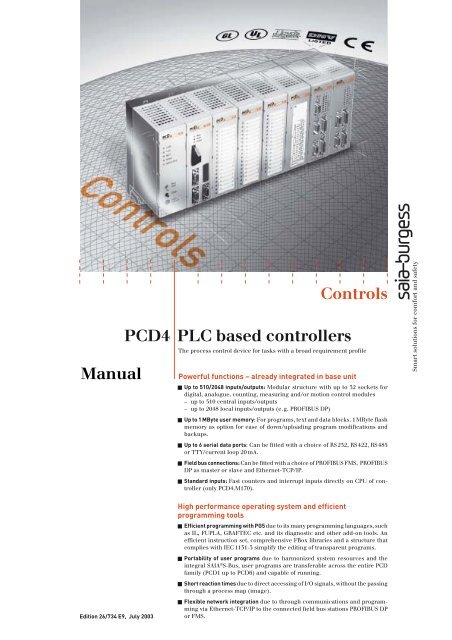
Manual<br />
PCD4 PLC based controllers<br />
Controls<br />
The process control device for tasks with a broad requirement profile<br />
Powerful functions – already integrated in base unit<br />
! Up to 510/2048 inputs/outputs: Modular structure with up to 32 sockets for<br />
digital, analo gue, counting, measuring and/or motion control modules<br />
– up to 510 central inputs/outputs<br />
– up to 2048 local inputs/outputs (e. g. PROFIBUS DP)<br />
! Up to 1 MByte user memory: For programs, text and data blocks. 1 MByte flash<br />
memory as option for ease of down/uploading program modifications and<br />
backups.<br />
! Up to 6 serial data ports: Can be fitted with a choice of RS 232, RS 422, RS 485<br />
or TTY/current loop 20 mA.<br />
! Field bus connections: Can be fitted with a choice of PROFIBUS FMS, PROFIBUS<br />
DP as master or slave and Ethernet-TCP/IP.<br />
! Standard inputs: Fast counters and interrupt inputs directly on CPU of controller<br />
(only PCD4.M170).<br />
Smart solutions for comfort and safety<br />
Edition 26/734 E9, July 2003<br />
High performance operating system and efficient<br />
programming tools<br />
! Efficient programming with PG5 due to its many programming languages, such<br />
as IL, FUPLA, GRAFTEC etc. and its diagnostic and other add-on tools. An<br />
efficient instruction set, comprehensive FBox libraries and a structure that<br />
complies with IEC 1131-3 simplify the editing of transparent programs.<br />
! Portability of user programs due to harmonized system resources and the<br />
integral SAIA ® S-Bus, user programs are transferable across the entire PCD<br />
family (PCD1 up to PCD6) and capable of running.<br />
! Short reaction times due to direct accessing of I/O signals, without the passing<br />
through a process map (image).<br />
! Flexible network integration due to through communications and programming<br />
via Ethernet-TCP/IP to the connected field bus stations PROFIBUS DP<br />
or FMS.
The adaptive controller platform<br />
The PCD4 series is an extremely flexible system. From the minimum system with<br />
the simplest processor, one serial interface, a low-cost power supply module<br />
and 2 I/O modules, through to the fully equipped system with up to 32 I/O and<br />
function modules, processor module ..M170, up to 6 independent serial interfaces<br />
or SAIA ® S-Bus, PROFIBUS FMS/DP or Ethernet-TCP/IP network connections. The<br />
system can be assembled in one go, or expanded in stages.<br />
All modules are in the form of equal sized cassettes. Cassette modules are plugged<br />
into the appropriate bus modules. The bus modules are in turn snapped onto<br />
mounting rails and connected together to form the system bus. Connections to<br />
the external process are wired to the bus modules, which means that cassette<br />
modules can be inserted or removed without affecting the wiring.<br />
Power supply<br />
modules Page 10<br />
Processor and<br />
public memory modules Page 6<br />
SAIA ® S-Bus (RS 485)<br />
The efficient protocol for this master-slave network is supported<br />
by every PCD both as master and as slave. Economical design across a<br />
serial RS 485 data port.<br />
Pages 8/9<br />
Combined bus module PCD4.C340<br />
with sockets for processor module, power supply module, 4 I/O modules<br />
and 3 sockets for serial data ports.<br />
Page 7<br />
Serial data ports<br />
sockets A1, A2, A3 on PCD4.C340<br />
up to 3 serial data ports as RS 422/RS 485, RS 485<br />
electrically isolated, RS 232 for modem or TTY/<br />
current loop 20 mA.<br />
Pages 8/9<br />
A1<br />
A2<br />
A3<br />
Flexible and modular I/O level using bus modules<br />
The I/O bus modules with 2 or 6 module sockets allow expansion up to 510<br />
inputs/outputs or 32 I/O modules.<br />
Page 7<br />
Digital input/output modules Pages 11–13 Analogue input/output modules Pages 14–16
PCD4<br />
up to 428 KBytes<br />
user memory as<br />
RAM or EPROM<br />
Page 5<br />
Processor module<br />
PCD4.M170 Page 6<br />
User memory<br />
1 MByte RAM and plug-on flash card for saving<br />
user memory.<br />
Pages 4/5<br />
Field bus connections<br />
sockets B1 and/or B2<br />
PROFIBUS FMS / DP: For both networks<br />
various modules are available as master<br />
or slave, also with additional RS 485 serial<br />
data port.<br />
Pages 8/9<br />
Serial data ports<br />
socket B2<br />
Counting, measuring and motion control modules Pages 18–20<br />
Ethernet-TCP/IP socket B2<br />
2 × RS 232 or RS 232 for modem, RS 232 and<br />
RS 422/RS 485<br />
Pages 8/9<br />
Intelligent co-processor module with fast<br />
dual-port RAM interface to the CPU, Ethernet<br />
10 Base-T/100 Base-TX. SAIA ® S-Bus with UDP/IP<br />
for PG5⇔PCD communication and PCD⇔PCD<br />
multimaster communication. Trans mission and<br />
receipt of TCP and UDP data packages for<br />
communication with any choice of system.<br />
Pages 8/9<br />
Manual operation modules Page 17<br />
System overview: Hardware
<strong>Saia</strong>-Burgess Controls Ltd. I<br />
Manual PCD4<br />
SAIA®Programmable Control Devices<br />
<strong>Saia</strong>-Burgess Controls Ltd.. All rights reserved<br />
HB-PCD4 26/734 E9, Chapter 5.1 07.2003<br />
Subject to technical changes<br />
Manual PCD4 26/734 E9-AT I General I 19.06.03
II<br />
<strong>Saia</strong>-Burgess Controls Ltd.<br />
Updates<br />
Chronology<br />
Date Chapter Page Description<br />
20.06.03 5 5.1-1 to -44 PCD4.M170 with 1 MByte flash card<br />
20.06.03 5 5.1-30, 39 Reference to termination box PCD7.T160<br />
Manual PCD4 26/734 E9-AT I General I 19.06.03
<strong>Saia</strong>-Burgess Controls Ltd.<br />
III<br />
Reliability and safety of electronic controllers<br />
Anlagen- bzw. Maschinenbauer<br />
<strong>Saia</strong>-Burgess Controls Ltd. is a company which devotes the greatest care to the design,<br />
development and manufacture of its products:<br />
· state-of-the-art technology<br />
· compliance with standards<br />
· ISO 9001 certification<br />
· international approvals: e.g. Germanischer Lloyd,<br />
United Laboratories (UL), Det Norske Veritas, CE mark ...<br />
· choice of high-quality componentry<br />
· quality control checks at various stages of production<br />
· in-circuit tests<br />
· run-in (burn-in at 85°C for 48h)<br />
Despite every care, the excellent quality which results from this does have its limits. It is<br />
therefore necessary, for example, to reckon with the natural failure of components. For this<br />
reason <strong>Saia</strong>-Burgess Controls Ltd. provides a guarantee according to the "General terms and<br />
conditions of supply".<br />
The plant engineer must in turn also contribute his share to the reliable operation of an<br />
installation. He is therefore responsible for ensuring that controller use conforms to the technical<br />
data and that no excessive stresses are placed on it, e.g. with regard to temperature ranges,<br />
overvoltages and noise fields or mechanical stresses.<br />
In addition, the plant engineer is also responsible for ensuring that a faulty product in no case<br />
leads to personal injury or even death, nor to the damage or destruction of property. The<br />
relevant safety regulations should always be observed. Dangerous faults must be recognized by<br />
additional measures and any consequences prevented. For example, outputs which are<br />
important for safety should lead back to inputs and be monitored from software. Consistent use<br />
should be made of the diagnostic elements of the PCD, such as the watchdog, exception<br />
organization blocks (XOB) and test or diagnostic instructions.<br />
If all these points are taken into consideration, the SAIA PCD will provide you with a modern,<br />
safe programmable controller to control, regulate and monitor your installation with reliability for<br />
many years.<br />
Manual 26/737 PCD2 E9 AT I General I 20.06.03
<strong>Saia</strong>-Burgess Controls Ltd. 1-3<br />
1 Read me<br />
1.1 About ourselves<br />
<strong>Saia</strong>-Burgess Controls Ltd (SBC) is a medium-sized European controls technology<br />
company. SBC is committed to the values, standards and culture of PLC engineering.<br />
All hardware, operating systems, software tools, CPUs, interfaces, etc. have been<br />
developed by SBC itself and are marketed as embedded controls.<br />
With full technical knowledge of all system elements and with quality-oriented<br />
business processes, SBC is equipped to provide unique, custom solutions regarding<br />
range of use, functionality, openness, flexibility, reliability and price.<br />
These core competencies, combined with innovative strength, a broad product range<br />
and a readiness to implement special customer requests rapidly, have made SBC the<br />
attractive, competitive partner of choice for a large number of international customers.<br />
Chapter 1 I 26/737-1 E2 Read me I 20.06.03<br />
PCD-K1-RM E3, 20.06.03
1-4 <strong>Saia</strong>-Burgess Controls Ltd.<br />
1.2 Product and documentation concept<br />
The SAIA ® PCD product range is rigorously modular in structure. It demonstrates a<br />
clear hierarchy of systems, sub-systems, functions and diverse accessories. Fully<br />
developed software tools allow the efficient creation of user programs.<br />
All SAIA ® PCD systems ( up to PCD6) work with the same operating system. The<br />
PCD systems communicate easily with each other and PCD user programs run on all<br />
systems.<br />
PCDn xx7 series controllers have a special operating system. This enables them to<br />
be programmed with Siemens ® STEP ® 7 and to communicate readily with the<br />
corresponding systems of other manufacturers.<br />
SAIA ® PCD customer documentation comprises pre-sales and after-sales<br />
documents that complement each other. As a rule, they are published in three<br />
language versions (German, English, French).<br />
Technical information Manuals References<br />
Technical Information (TI) documents offer overviews of a system (e.g. the SAIA ®<br />
PCD operating system OS), sub-system (e.g. PCD2) or product family with common<br />
features (e.g. digital I/O modules, etc.).<br />
TIs have been designed as pre-sales documents. They describe the system or<br />
product features and contain all the selection criteria necessary for a preliminary<br />
project. They offer the prospective customer more information than a normal<br />
brochure.<br />
TIs are available free-of-charge as brochures or in electronic form (on CD for a token<br />
fee or free of charge via Internet http://www.sbc-support.ch).<br />
Manuals are after-sales documents. They contain all the detailed information and<br />
application examples necessary for the efficient realization of a project. Manuals are<br />
available to the SAIA ® PCD customer in electronic form on CD (for a token fee) and<br />
free of charge via Internet http://www.sbc-support.ch.<br />
Chapter 1 I 26/737-1 E2 Read me I 20.06.03<br />
PCD-K1-RM E3, 20.06.03
<strong>Saia</strong>-Burgess Controls Ltd. 1-5<br />
References describe projects that have been successfully realized with SAIA ® PCDs<br />
(after-sales). The solutions outlined in them will provide many ideas for the use of<br />
SAIA ® PCDs in similar projects (pre-sales, closing the loop with the TI). References<br />
are available free-of-charge as brochures or in electronic form (on CD or via Internet<br />
http://www.sbc-support.ch). Please read also our Controls News published on<br />
internet side: http://www.controls-news.ch.<br />
P documentation (P = preliminary) describes new or extensively redeveloped<br />
products. After extensive internal testing of function and integration, these products<br />
are supplied to external commercial partners for field trials under more difficult<br />
conditions. P documentation is provided for these field trials. Improvements<br />
suggested by these external partners influence the definitive documentation. P<br />
documents can be requested as PDF files and some are available free-of-charge via<br />
Internet http://www.sbc-support.ch.<br />
1.3 Technical support<br />
Any questions that you cannot answer by referring to the documentation will be dealt<br />
with promptly and reliably for you by the SAIA ® PCD <strong>Support</strong> Team. The team is<br />
based in Switzerland and can be reached by telephoning ++41 26 672 72 72 or by<br />
E-Mail pcdsupport@saia-burgess.com.<br />
The addresses of <strong>Saia</strong>-Burgess sales companies and agents for other sales areas<br />
can be found under http://www.saia-burgess.com.<br />
1.4 Workshops, training literature<br />
Interesting, informative SAIA ® PCD workshops offer technically qualified people the<br />
opportunity to make valuable contacts and extend their technical knowledge of the<br />
PCD, taking home with them both the training literature and the solutions produced<br />
collaboratively during the workshop.<br />
Workshops are your route to joining the large group of enthusiastic SAIA ® PCD users.<br />
Current workshop programs are among a wealth of other useful information to be<br />
found under http://www.sbc-support.ch/<br />
Chapter 1 I 26/737-1 E2 Read me I 20.06.03<br />
PCD-K1-RM E3, 20.06.03
1-6 <strong>Saia</strong>-Burgess Controls Ltd.<br />
1.5 Navigation in electronic-based PDF documents<br />
To navigate in PDF documents, press the "hand tool (H)" button.<br />
1.5.1 Structure of PCD manuals<br />
PCD manuals comprise a "General section" and the chapter sections or sub-sections.<br />
These in turn comprise a number of document modules. The latter are uniquely<br />
identified with their own number, version details and issue date. This is necessary<br />
because many document modules are used in more than one manual.<br />
Blue web links, e.g. http://www.sbc-support.ch/ serve to establish an Internet<br />
connection.<br />
1.5.2 Navigation<br />
Navigation is via bookmarks. Clicking the mouse on “+” will display ancillary<br />
bookmarks.<br />
The pictograms offer further navigation possibilities (after clicking the mouse on the<br />
appropriate index card), as do the "Contents lists” of individual chapters.<br />
(Scrolling with the arrow keys<br />
or<br />
takes a little longer. They are<br />
practical for going to the title page or to the back page, which has the ordering<br />
information and addresses with blue web links.)<br />
A mouse click on the desired chapter heading will take you to the beginning of that<br />
chapter. From there, it is best to use the arrow keys for scrolling, or the links identified<br />
by blue key words.<br />
Right-clicking once on the mouse will open a menu with various options (e.g. "Go to<br />
previous view"). Normally, bookmarks will be a faster way of arriving at the starting<br />
point or any new destination (e.g. another chapter).<br />
1.5.3 Summary of navigational aids<br />
• Bookmarks (on left margin of screen, outside the document)<br />
• Any pictograms (after clicking mouse on index card)<br />
• Contents lists with links to topics required<br />
• Blue web links, for establishing Internet connections quickly<br />
• Key words marked blue, for accessing more detailed information<br />
(within any one chapter section or subsection)<br />
Chapter 1 I 26/737-1 E2 Read me I 20.06.03<br />
PCD-K1-RM E3, 20.06.03
<strong>Saia</strong>-Burgess Controls Ltd. 1-7<br />
1.6 Icons<br />
In manuals, this symbol refers the reader to further information in other manuals or<br />
technical information documents (e.g. “For details see TI 26/365”).<br />
As a rule there is no direct link to such documents.<br />
This symbol warns the reader of the risk to components from electrostatic<br />
discharges caused by touch.<br />
Recommendation: at least touch the Minus of the system (cabinet of PGU<br />
connector) before coming in contact with the electronic parts. Better is to use a<br />
grounding wrist strap with its cable attached to the Minus of the system.<br />
The caution sign accompanies instructions that must always be followed.<br />
Chapter 1 I 26/737-1 E2 Read me I 20.06.03<br />
PCD-K1-RM E3, 20.06.03
1-8 <strong>Saia</strong>-Burgess Controls Ltd.<br />
Chapter 1 I 26/737-1 E2 Read me I 20.06.03 PCD-K1-RM E3, 20.06.03
PCD4<br />
Contents<br />
Contents<br />
Page<br />
1. The modular system structure of the PCD4 series<br />
1.1 Block diagram 1-2<br />
1.2 System information 1-4<br />
2. The mechanical structure of the PCD4 series<br />
2.1 Arrangement of the bus modules 2-3<br />
2.2 PCD4 assembly in one row for maximum of 256 I/O 2-4<br />
2.3 PCD4 assembly in two rows for maximum of 256 I/O 2-5<br />
2.4 PCD4 assembly for a maximum of 512 I/O 2-6<br />
2.5 Addressing input and output modules 2-8<br />
2.6 Coding the module edge connectors 2-10<br />
3. The bus modules of the PCD4 series<br />
3.1 Bus modules PCD4.C1x0 for supply and processor 3-3<br />
3.2 Screw terminal assignments of the PCD4.C1x0 bus<br />
modules for supply and processor 3-5<br />
3.3 Screw terminal assignments of the PCD4.C1x0 bus<br />
modules for communication interfaces 3-6<br />
3.3.1 Interface RS 232 3-6<br />
3.3.2 Interface 20 mA current loop 3-9<br />
3.3.3 Interface RS 422 3-11<br />
3.3.4 Interface RS 485 3-12<br />
3.4 Bus module PCD4.C340 for supply, processor,<br />
4 I/O modules and 3 serial interfaces 3-15<br />
3.4.1 RS 422 / RS 485 with module PCD7.F110 3-18<br />
3.4.2 RS 232 with module PCD7.F120 3-20<br />
3.4.3 20 mA current loop with module PCD7.F130 3-21<br />
3.4.4 RS 485, electrically isolated, with PCD7.F150 3-23<br />
3.5 Bus modules PCD4.C2x0 for input/output modules 3-24<br />
3.6 Bus module PCD4.C225 for coupling the PCD4 I/O<br />
modules in expansion to a PCD2.M… 3-25<br />
26/734 E7 (D4-00-E.DOC) © SAIA-Burgess Electronics Ltd. Page 1
Contents<br />
PCD4<br />
Page<br />
3.7 Power supply and connection plan 3-27<br />
3.7.1 External power supply 3-27<br />
3.7.2 Grounding plan 3-29<br />
3.7.3 Connection plan 3-30<br />
3.8 Quick guide to handling the PCD4 3-32<br />
3.8.1 Bus module assembly 3-32<br />
3.8.2 Entering a lamp flasher program 3-34<br />
3.8.3 Outputting texts to the PCD7.D202 terminal<br />
via the RS 232 serial interface 3-35<br />
4. The earlier processor modules of the PCD4 series<br />
4.1 Points common to all processor modules 4-2<br />
4.1.1 General 4-2<br />
4.1.2 Shared characteristics 4-3<br />
4.1.3 Operating states of the processor module 4-4<br />
4.1.4 "RESET OUTPUT" - "ENABLE" jumper 4-5<br />
4.1.5 "HALT/CLEAR" - "ENABLE" jumper 4-6<br />
4.1.6 The "EXTERNAL RESET" function 4-6<br />
4.1.7 The firmware 4-7<br />
4.1.8 The PGU serial interface 4-7<br />
4.2 The processor modules PCD4.M110 and PCD4.M1x5<br />
with 1 processor 4-9<br />
4.2.1 Front panel and board layout 4-9<br />
4.2.2 Processor module PCD4.M110 4-10<br />
4.2.3 Interfaces of processor module PCD4.M125 4-10<br />
4.2.4 Interfaces of processor module PCD4.M145 4-11<br />
4.3 The processor module PCD4.M445 with 2 processors<br />
and an additional PROFIBUS-FMS co-processor 4-13<br />
4.3.1 Front panel and board layout 4-13<br />
4.3.2 Block diagram 4-15<br />
4.3.3 Serial interfaces of the PCD4.M445 processor 4-16<br />
4.3.4 The PROFIBUS-FMS interface 4-17<br />
4.3.5 PROFIBUS-FMS utilities and data types 4-17<br />
4.3.6 SAIA ® PCD PROFIBUS configurator 4-18<br />
4.3.7 PROFIBUS-FMS connection 4-18<br />
4.4 Summary of bus and processor module combinations 4-22<br />
Page 2 © SAIA-Burgess Electronics Ltd. (D4-00-E.DOC) 26/734 E7
PCD4<br />
Contents<br />
Page<br />
5. CPU options<br />
Contents chapter 5.1<br />
6. The public memory modules PCD7.R…<br />
6.1 Common specifications 6-2<br />
6.2 The battery 6-3<br />
6.3 PCD7.R110 with user memory up to 256 KBytes 6-4<br />
6.4 PCD7.R310 with user memory up to 428 KBytes 6-6<br />
7. The power supply modules PCD4.N2..<br />
7.1 General 7-1<br />
7.2 Use of the “Watch Dog” 7-5<br />
7.3 Power requirements of the PCD4 modules 7-6<br />
8. Digital input/output modules<br />
8.1 PCD4.E110/E111 (without electrical isolation)<br />
Module with 16 digital inputs 8-3<br />
8.2 PCD4.E600/E601 (with electrical isolation)<br />
Module with 16 digital inputs 8-7<br />
8.3 PCD4.A200 (with contact protection)<br />
Output module with 8 relay contacts, "normally. open" 8-9<br />
8.4 PCD4.A250 (without contact protection)<br />
Output module with 16 relay contacts, "normally. open" 8-15<br />
8.5 PCD4.A350 (with electrical isolation)<br />
Module with 8 digital outputs, 24 VDC / 2 A 8-21<br />
8.6 PCD4.A400 (without electrical isolation)<br />
Module with 16 digital outputs, 0.5 A 8-25<br />
8.7 PCD4.A410 (with electrical isolation)<br />
Module with 16 digital outputs, 0.5 A 8-27<br />
8.8 PCD4.B900/B901 (without electrical isolation)<br />
Digital I/O module, with 16 inputs and 16 outputs 8-29<br />
26/734 E7 (D4-00-E.DOC) © SAIA-Burgess Electronics Ltd. Page 3
Contents<br />
PCD4<br />
Page<br />
9. Analogue input/output modules<br />
9.1 PCD4.W100<br />
Analogue input/output module, 6 channels (4I + 2O),<br />
12 bit resolution 9-3<br />
9.2 PCD4.W300<br />
Analogue input module, 8 channels,<br />
12 bit resolution and sign bit 9-19<br />
9.3 PCD4.W400<br />
Analogue output module, 8 channels,<br />
8 bit resolution 9-35<br />
9.4 PCD4.W500 (with galvanic isolation)<br />
Analogue input module, 8 channels,<br />
12/15 bit resolution 9-41<br />
9.5 PCD4.W600 (with galvanic isolation)<br />
Analogue output module, 8 channels,<br />
12 bit resolution 9-45<br />
10. Manual Operation modules<br />
10.1 PCD4.A810<br />
Digital output module with manual overrides, 1 level 10-3<br />
10.2 PCD4.A820<br />
Digital output module with manual overrides, 2 levels 10-13<br />
10.3 PCD4.W800<br />
Analogue output module with manual overrides 10-25<br />
11. Fast counter and positioning modules<br />
12. Dimensions of the PCD4<br />
13. PCD4 - Hardware type designations<br />
Page 4 © SAIA-Burgess Electronics Ltd. (D4-00-E.DOC) 26/734 E7
PCD4<br />
The modular system structure of the PCD4 series<br />
1. The modular system structure of the<br />
PCD4 series<br />
The modular design of PCD4 series offers great flexibility. Within addressing<br />
limits, a range of processor and memory modules, power supplies,<br />
digital I/O modules, analogue I/O modules, fast counter modules<br />
and DC and stepper motor controllers can be combined to satisfy almost<br />
any application.<br />
The system can be built up in stages : from the minimal system, with one<br />
processor, one serial interface and a power supply, to the full system with<br />
two processors, four serial interfaces, 32 add-on modules and a S-Bus or<br />
a PROFIBUS connection.<br />
All modules are produced in the form of cartridges with the same dimensions.<br />
Each cartridge is plugged into a bus module. The bus modules are<br />
snapped onto mounting rails, and connect electrically to form the PCD4<br />
bus.<br />
Apart from mechanical design, the PCD4 differs from the PCD1- PCD2<br />
and PCD6 series in only four areas :<br />
PCD1 PCD2 PCD4 PCD6<br />
Max. Inputs/Outputs 64 256 512 5120<br />
Number of CPU’s 1 1 1 or 2 1 to 6<br />
Nb. of serial interfaces 1 to 2 1 to 4 1 to 4 5 to 30<br />
User memory 17 to 140 KBytes 32 to 640 KBytes 64 to 428 KBytes 256 KB to 1 MBytes<br />
The PCD4 has the same number of flags (8192), timers/counters (1600),<br />
registers (4096), program blocks, texts and data blocks as the PCD6 series.<br />
The instruction sets are identical, and the same programming tools<br />
are used for all series.<br />
26/734 E7 (D4-10-E.DOC) © SAIA-Burgess Electronics Ltd. Page 1-1
The modular system structure of the PCD4 series<br />
PCD4<br />
1.1 Block diagram<br />
The following block diagram shows the internal structure of the<br />
PCD4 system :<br />
1 - 4 DATALINES<br />
PROFIBUS<br />
SUPPLY<br />
WD<br />
CPUO<br />
CPU 1<br />
ex LAN 2<br />
ARBITRATOR<br />
SERIAL<br />
INTERFACES<br />
I/O<br />
0 - 511<br />
P C D 4 - B U S<br />
M<br />
E<br />
M<br />
O<br />
R<br />
Y<br />
M<br />
A<br />
P<br />
P P<br />
Tx Tx<br />
DB DB<br />
CPUO CPU 1<br />
F<br />
VOL<br />
NVOL<br />
F<br />
T<br />
VOL<br />
...<br />
NVOL<br />
C<br />
R<br />
NVOL<br />
CLOCK<br />
NVOL<br />
PUBLIC-MEMORY-<br />
MODULE PCD7.R<br />
USER MEMORY<br />
PUBLIC ELEMENTS<br />
P Program F Flags CLOCK Date-time<br />
TX Text T Timers VOL Volatile<br />
DB Data blocks C Counters NVOL Non-volatile<br />
R Registers<br />
The power supply module supplies the voltages for the internal electronics.<br />
The supervisory "Watch dog" timer (WD) is also located in this<br />
module.<br />
The memory module, which is plugged into the processor module,<br />
contains the memory for user programs, texts and data blocks in the form<br />
of RAM or EPROM, with the necessary memory map. It also holds all<br />
shared resources : flags, timers, counters, data registers and the real-time<br />
clock.<br />
Page 1-2 © SAIA-Burgess Electronics Ltd. (D4-10-E.DOC) 26/734 E7
PCD4<br />
The modular system structure of the PCD4 series<br />
As the diagram shows, the 8192 flags (F) can be defined as volatile<br />
(VOL) or non-volatile (NVOL) flags, as desired. The user can also select<br />
which of the 1600 x 32-bit timer/counters will be timers (T) and which<br />
will be counters (C) in accordance with his requirements. The timers are<br />
always volatile, the counters are always non-volatile. The 4096 x 32 bit<br />
data registers (R) are always non-volatile. Flags, timers, counters and<br />
registers can be accessed by both processors, if present.<br />
The user memory for programs, texts and data blocks (P / TX / DB)<br />
on the memory module is battery-backed in the RAM version. The "Configure"<br />
programming utility carries out the allocation of memory for user<br />
program and text for one or two processors, according to the application.<br />
The PCD4 bus, formed by the bus modules, extends through the whole<br />
system as the block diagram shows. This bus provides the data path between<br />
all system components and is used by the processors and all addon<br />
I/O modules. The internal power is also supplied via this bus.<br />
The positions to the right of the processor module can be fitted with I/O<br />
modules for digital and analogue signals, or with special modules such as<br />
the fast counters or stepper motor controllers.<br />
26/734 E7 (D4-10-E.DOC) © SAIA-Burgess Electronics Ltd. Page 1-3
The modular system structure of the PCD4 series<br />
PCD4<br />
1.2 System information<br />
Processor module<br />
Processing time<br />
User memory<br />
Number of I/Os<br />
Serial interfaces<br />
Serial interface types<br />
Flags<br />
Timers/counters<br />
Timebase for timers<br />
Data registers<br />
Data formats<br />
Index register<br />
With 1 or 2 processors for 1 bit or word processing<br />
and communication. Or with1 processor<br />
and a co-processor for connection to the<br />
PROFIBUS-FMS network.<br />
Approx. 4 µs per bit instruction<br />
(read directly, without a process copy).<br />
Either battery-backed RAM, or<br />
EPROM memory. Total 64K x 32 bits.<br />
This allows 64K of user program lines or 256K<br />
of text characters, or a mixture of both, and additional<br />
172 KByte RAM for TX and DB.<br />
Max. 512 in up to 32 modules<br />
(each module has 8 or 16 I/Os)<br />
1 to 4 independent serial channels<br />
RS 232, RS 422 or RS 485 as well as 20mA<br />
current loop.<br />
Serial interface 0 is always RS232, since it is<br />
used for connection to the programming unit.<br />
8192 x 1 bit<br />
(divided between volatile and non-volatile)<br />
1600 x 31 bits, programmable division.<br />
(timers are always volatile, counters are<br />
non-volatile.<br />
Programmable from 10ms to 10 seconds<br />
4096 x 32 bits (non-volatile),<br />
can be loaded by the user program, or via the<br />
programming unit from/to diskette.<br />
Additional max. 32K registers in data blocks if<br />
the user memory (RAM or EPROM) is used.<br />
Decimal, hexadecimal, BCD, binary or floating<br />
point (exponential representation)<br />
17 x 13 bits per processor<br />
(1 for each COB and 1 for all XOBs)<br />
Page 1-4 © SAIA-Burgess Electronics Ltd. (D4-10-E.DOC) 26/734 E7
PCD4<br />
The modular system structure of the PCD4 series<br />
Cyclic Organization<br />
Blocks (COB)<br />
Exception Organization<br />
Blocks (XOB)<br />
Program Blocks<br />
(PB)<br />
Function Blocks<br />
(FB)<br />
Sequential Blocks<br />
(SB)<br />
Texts (TX) and<br />
data blocks (DB)<br />
Special texts<br />
Date/time<br />
(hardware clock)<br />
Operating<br />
temperature<br />
16 per processor<br />
Up to 32 per processor<br />
300 per processor<br />
1000 per processor, with run-time parameters<br />
32 per processor (for GRAFTEC programming<br />
with 2000 steps and 2000 transitions with up to<br />
32 active parallel branches)<br />
8000 per processor,<br />
with up to 3 levels of sub-texts<br />
For output of date, time, logic states, contents<br />
of registers and counters in various formats<br />
(also with decimal point),<br />
addressed directly or indirectly.<br />
Week, day of week, year, month, date,<br />
hour, minute, second.<br />
Precision :<br />
Better than 60s/month<br />
Battery power reserve : 2 months<br />
0...55°C (below modules)<br />
Resistance to inter- In accordance with IEC 801-4<br />
ference of digital I/Os Class III (4000 V)<br />
and power supply<br />
Supply voltages For supply module : 24 VDC<br />
(nominal) For I/Os 24 VDC<br />
26/734 E7 (D4-10-E.DOC) © SAIA-Burgess Electronics Ltd. Page 1-5
The modular system structure of the PCD4 series<br />
PCD4<br />
Notes :<br />
Page 1-6 © SAIA-Burgess Electronics Ltd. (D4-10-E.DOC) 26/734 E7
PCD4<br />
The mechanical structure of the PCD4 series<br />
2. The mechanical structure of the PCD4 series<br />
As the following diagrams show, the clip-on bus modules are connected<br />
together to form the backbone and bus of the PCD4.<br />
The cartridge-style power supply, processor and I/O modules are plugged<br />
into these bus modules.<br />
Inputs/Outputs modules<br />
o<br />
o<br />
o<br />
o<br />
o<br />
o<br />
o<br />
SAIA<br />
O<br />
O<br />
The bus modules Supply Processor module Bus module with<br />
clip onto this module for with memory screw terminals<br />
DIN rail connection module inserted<br />
to 24 VDC<br />
A double mounting rail (35 mm, DIN/EN 50022) is used to support the<br />
bus modules. The required number of bus modules are snapped onto this<br />
rail and connected together electrically and mechanically (see drawing on<br />
next page). External connections should be wired next, using the screw<br />
terminals.<br />
After completion of assembly and wiring, insert and fasten the supply<br />
module, the processor module and up to 32 add-on I/O or special modules.<br />
26/734 E7 (D4-20-E.DOC) © SAIA-Burgess Electronics Ltd. Page 2-1
The mechanical structure of the PCD4 series<br />
PCD4<br />
The sequence of assembly is shown in these diagrams :<br />
Assembly PCD4<br />
Disassembly PCD4<br />
1<br />
4<br />
7<br />
2<br />
5<br />
8<br />
3<br />
6<br />
9<br />
1. Pull the retaining clip<br />
down and slot the bus<br />
module onto the DIN rail<br />
2. Push the retaining clip<br />
upwards<br />
3. Connect the wires with<br />
a no. 1 screwdriver<br />
4. Pull up the module<br />
retaining clip<br />
5. Insert the module<br />
6. Push the module retaining<br />
clip downwards<br />
7/8. Pull up the module<br />
retaining clip using<br />
a no. 1 screwdriver<br />
9. Unplug the module<br />
Important note : (risk of damage)<br />
Modules must never be inserted onto or removed from<br />
the bus module when the supply voltage is present !<br />
Page 2-2 © SAIA-Burgess Electronics Ltd. (D4-20-E.DOC) 26/734 E7
PCD4<br />
The mechanical structure of the PCD4 series<br />
2.1 Arrangement of the bus modules<br />
Bus connector<br />
for I/O modules<br />
Continuous I/O bus<br />
connector or cable<br />
Edge connector for<br />
add-on I/O modules<br />
Connector between<br />
two bus modules with<br />
cover plate<br />
Bus module type<br />
PCD4.C1x0 for supply<br />
and processor modules<br />
Tab for unclipping<br />
bus modules<br />
Bus modules type PCD4.C2x0<br />
for add-on I/O modules<br />
The bus modules for the supply and processor modules must each be installed<br />
on the left side of every assembled PCD4 (PCD4.C1x0 or ..C340).<br />
The I/O bus modules (PCD4.C2x0) are placed on the right.<br />
To unclip and remove a bus module, the lower tab must be pulled downwards.<br />
Connection between bus modules is via connector plugs and the accessories<br />
which accompany every bus module<br />
(re-order with no. 4 421 8698 0).<br />
After insertion of the bus connector, the cover plate (supplied as an accessory)<br />
should be screwed down with two screws. This metal cover protects<br />
the bus and ensures good mass distribution throughout the system.<br />
Bus connector plug<br />
(re-order no. 4 421 8698 0)<br />
26/734 E7 (D4-20-E.DOC) © SAIA-Burgess Electronics Ltd. Page 2-3
The mechanical structure of the PCD4 series<br />
PCD4<br />
2.2 PCD4 assembly in one row for a maximum of 256 I/O *)<br />
N M<br />
218<br />
Number of<br />
I/O modules<br />
2<br />
Address<br />
range<br />
0 to 31<br />
N M<br />
327<br />
4<br />
0 to 63<br />
N M<br />
436<br />
6<br />
0 to 95<br />
N M<br />
8<br />
0 to 127<br />
545<br />
N M<br />
10<br />
0 to 159<br />
654<br />
N M<br />
12<br />
0 to 191<br />
763<br />
N M<br />
14<br />
0 to 223<br />
872<br />
N M<br />
16<br />
0 to 254<br />
981<br />
The PCD4 series allows from 2 to 16 add-on I/O modules to be arranged<br />
in one row. For this purpose, bus modules with sites for either 2 add-on<br />
modules (PCD4.C220) or 6 add-on modules (PCD4.C260) are available.<br />
If possible, the above combinations should be used.<br />
Note that the fewest possible bus connectors should be used. The upper<br />
limit is around 5 connectors. This includes the connecting cable in case<br />
of assembly in two rows, see next page.<br />
*) This number can be doubled by use of the digital ..B900 modules<br />
(16 inputs + 16 outputs).<br />
Page 2-4 © SAIA-Burgess Electronics Ltd. (D4-20-E.DOC) 26/734 E7
PCD4<br />
The mechanical structure of the PCD4 series<br />
2.3 PCD4 assembly in two rows for a maximum of 256 I/O *)<br />
o<br />
o<br />
o<br />
o<br />
o<br />
o<br />
o<br />
O<br />
O<br />
Bus extension cable :<br />
PCD4.K200 , length 100 cm<br />
PCD4.K210 , length 80 cm<br />
If there is insufficient space for all I/O modules in one row, they can be<br />
arranged in a second row above or below the row which contains the<br />
processor module.<br />
The bus extension cable PCD4.K200 or ..K210 is required for extending<br />
the bus. This is fitted into the bus connector and secured with a screw.<br />
Since it is well screened, the bus extension cable can be layed in the cable<br />
channel of the installation wiring. The length of the bus extension cable<br />
must not be changed.<br />
Addressing the I/O modules continues via the bus extension cable in the<br />
same way, as if they were assembled in one row.<br />
*) This number can be doubled by use of the digital ..B900 modules<br />
(16 inputs + 16 outputs).<br />
26/734 E7 (D4-20-E.DOC) © SAIA-Burgess Electronics Ltd. Page 2-5
The mechanical structure of the PCD4 series<br />
PCD4<br />
2.4 PCD4 assembly for a maximum of 512 I/O *)<br />
While paying attention to the internal power requirements placed on the<br />
power supply module, it is possible to add a maximum of 32 I/O modules,<br />
providing 512 I/Os (or more with ..B900 modules).<br />
Addressing from the basic package (consisting of N2.. and M.. to ..C1x0<br />
or ..C340 modules) is done on two sides :<br />
- right bus connector addresses 0 to 254<br />
- left bus connector addresses 256 to 510<br />
N2<br />
M...<br />
I/O addresses<br />
I/O addresses<br />
256 ... 510 0 ... 254<br />
Addresses 255<br />
and 511 are<br />
occupied by the<br />
watchdog<br />
PCD4.C1..<br />
With the help of two additional bus cables, the following assemblies can<br />
be constructed in two to four rows :<br />
• In 2 rows :<br />
2a) 2b)<br />
NM<br />
0 254<br />
256 510<br />
..K250<br />
256 510<br />
..K250<br />
N M<br />
0<br />
254<br />
*) The maximum number of I/O modules is limited by internal power<br />
requirements. The table in chapter 7 "Power Supply Modules" must<br />
be consulted.<br />
Page 2-6 © SAIA-Burgess Electronics Ltd. (D4-20-E.DOC) 26/734 E7
PCD4<br />
The mechanical structure of the PCD4 series<br />
• In 3 rows :<br />
3a) 3b)<br />
256<br />
..K260<br />
N<br />
M<br />
0<br />
254<br />
..K200 / 210<br />
..K260<br />
510<br />
..K200 / 210<br />
256<br />
(510)<br />
N M<br />
0<br />
(254)<br />
• In 4 rows :<br />
4a) 4b)<br />
256<br />
..K260<br />
N<br />
M<br />
0<br />
254<br />
..K200 / 210<br />
..K260<br />
510<br />
..K200 / 210<br />
256<br />
510<br />
..K200 / 210<br />
N M<br />
0<br />
..K200 / 210<br />
254<br />
The following spacing should be observed between rows of modules :<br />
Remarks :<br />
PCD4.K260<br />
PCD4.K250<br />
- Maximum length of 2.5 m<br />
between the CPU and the<br />
last I/O module.<br />
- Maximum 5 interconnections<br />
max.<br />
170<br />
max.<br />
170<br />
max. 530<br />
26/734 E7 (D4-20-E.DOC) © SAIA-Burgess Electronics Ltd. Page 2-7
The mechanical structure of the PCD4 series<br />
PCD4<br />
2.5 Addressing input and output modules<br />
o<br />
o<br />
o<br />
o<br />
o<br />
o<br />
o<br />
SAIA<br />
A<br />
E<br />
A<br />
E<br />
A<br />
E<br />
A<br />
E<br />
A<br />
E<br />
A<br />
O<br />
O<br />
0 16 32 48 64 80<br />
Address locations<br />
for I/O modules<br />
0 16 32 48 64 80<br />
15 31 47 63 79 95<br />
Label with<br />
base<br />
address<br />
Each add-on I/O module reserves 16 addresses. Starting with the base<br />
address 0 (zero) at the first module position to the right of the processor<br />
module, the addresses increase towards the right in steps of 16. The same<br />
also applies for modules which occupy only 8 addresses. If modules with<br />
8 addresses are used, 8 addresses are lost for each module.<br />
If the bus extension cable is used to form a second row of modules, addressing<br />
continues similarly in the second row.<br />
It is recommended that the sticky labels with base address 0, 16, 32, etc.<br />
are applied to the bus modules for each module position, so that each<br />
I/O module can be easily labelled.<br />
As shown in the preceding section, cables ..K250 and ..K260 can be used<br />
to expand addressing from 256 to 510.<br />
Caution :<br />
Since the Watch Dog (see chapter 7.2) uses addresses<br />
255 and 511, only digital I/O modules may be inserted in<br />
these fields.<br />
Analogue modules (types ..W) and counting or positioning<br />
modules (types ..H) cannot be run in the addresses<br />
ranges 240 to 255 and 496 to 511.<br />
Page 2-8 © SAIA-Burgess Electronics Ltd. (D4-20-E.DOC) 26/734 E7
PCD4<br />
The mechanical structure of the PCD4 series<br />
The numbered labels, which accompany the modules, serve to identify<br />
the I/O modules by address location. These labels slide onto the front of<br />
each module. On the left is the absolute address (belonging to the LED);<br />
on the right is the terminal number. (The terminal numbers are the same<br />
for every I/O module).<br />
After each address, a blank space is provided for writing the associated<br />
I/O name or reference. Analogue and other special modules have different<br />
labels.<br />
Sticky labels for the base addresses on the bus modules and front plates<br />
for the digital I/O modules for addresses 0...127 are supplied as accessories<br />
with every PCD4.C1x0 or PCD4.C340 bus module.<br />
Other sets are available :<br />
4'310'8567'0 for addresses 0 ... 127<br />
4'310'8568'0 for addresses 128 ... 255<br />
4'310'8569'0 for addresses 256 ... 511<br />
4'310'8570'0 for ..W and ..H modules<br />
PCD4.E10<br />
O 96.............0<br />
O 97.............1<br />
O 98.............2<br />
O 99.............3<br />
O 100............4<br />
O 101............5<br />
O 102............6<br />
O 103............7<br />
O 104............8<br />
O 105............9<br />
O 106..........10<br />
O 107..........11<br />
O 108..........12<br />
O 109..........13<br />
O 110..........14<br />
O 111..........15<br />
Absolute element address<br />
Terminal number<br />
Space for labelling<br />
26/734 E7 (D4-20-E.DOC) © SAIA-Burgess Electronics Ltd. Page 2-9
The mechanical structure of the PCD4 series<br />
PCD4<br />
2.6 Coding the module edge connectors<br />
To prevent the insertion of the wrong plug-in module, the edge connectors<br />
on the bus modules can be specially keyed. Each module type has an<br />
identification key in the form of slots cut into the edge connector, according<br />
to the following table :<br />
C1x0 /<br />
C2x0 / C340<br />
C340 Inputs Outputs Function modules<br />
N M E E E B A A A A A A W W W W W W H H H H<br />
2<br />
x<br />
0<br />
x<br />
x<br />
x<br />
1<br />
0<br />
x<br />
1<br />
1<br />
x<br />
6<br />
0<br />
x<br />
9<br />
0<br />
x<br />
2<br />
0<br />
0<br />
2<br />
5<br />
0<br />
3<br />
5<br />
0<br />
4<br />
x<br />
0<br />
8<br />
1<br />
0<br />
8<br />
2<br />
0<br />
1<br />
0<br />
0<br />
3<br />
0<br />
0<br />
4<br />
0<br />
0<br />
5<br />
0<br />
0<br />
6<br />
0<br />
0<br />
8<br />
0<br />
0<br />
1<br />
2<br />
0<br />
2<br />
x<br />
x<br />
3<br />
x<br />
x<br />
4<br />
x<br />
0<br />
A x x x x<br />
B x x<br />
C x x x x x x x<br />
D x x x x<br />
E x x x x x x x<br />
F x x x<br />
G x x x x x x<br />
H x x x<br />
I x x x<br />
K x x x<br />
L<br />
Keys are already inserted for the power supply and processor modules on<br />
the bus module PCD4.C1x0 or ..C340.<br />
For the I/O modules, the keys should be located according to the above<br />
table.<br />
Edge connector on<br />
bus module with inserted<br />
keys<br />
A<br />
B<br />
C<br />
D<br />
E<br />
F<br />
G<br />
H<br />
I<br />
K<br />
L<br />
PCD4.E100<br />
Page 2-10 © SAIA-Burgess Electronics Ltd. (D4-20-E.DOC) 26/734 E7
PCD4<br />
The mechanical structure of the PCD4 series<br />
Connecting terminals to I/O addresses<br />
Terminals<br />
Addresses for the modules PCD4.E110 / E600 / A400 / B900<br />
0 0 16 32 48 64 80 96 112<br />
1 1 17 33 49 65 81 97 113<br />
2 2 18 34 50 66 82 98 114<br />
3 3 19 35 51 67 83 99 115<br />
4 4 20 36 52 68 84 100 116<br />
5 5 21 37 53 69 85 101 117<br />
6 6 22 38 54 70 86 102 118<br />
7 7 23 39 55 71 87 103 119<br />
8 8 24 40 56 72 88 104 120<br />
9 9 25 41 57 73 89 105 121<br />
10 10 26 42 58 74 90 106 122<br />
11 11 27 43 59 75 91 107 123<br />
12 12 28 44 60 76 92 108 124<br />
13 13 29 45 61 77 93 109 125<br />
14 14 30 46 62 78 94 110 126<br />
15 15 31 47 63 79 95 111 127<br />
Terminals<br />
Addresses for the modules PCD4.E110 / E600 / A400 / B900<br />
0 128 144 160 176 192 208 224 240<br />
1 129 145 161 177 193 209 225 241<br />
2 130 146 162 178 194 210 226 242<br />
3 131 147 163 179 195 211 227 243<br />
4 132 148 164 180 196 212 228 244<br />
5 133 149 165 181 197 213 229 245<br />
6 134 150 166 182 198 214 230 246<br />
7 135 151 167 183 199 215 231 247<br />
8 136 152 168 184 200 216 232 248<br />
9 137 153 169 185 201 217 233 249<br />
10 138 154 170 186 202 218 234 250<br />
11 239 155 171 187 203 219 235 251<br />
12 140 156 172 188 204 220 236 252<br />
13 141 157 173 189 205 221 237 253<br />
14 142 158 174 190 206 222 238 254<br />
15 143 159 175 191 207 223 239 255<br />
26/734 E7 (D4-20-E.DOC) © SAIA-Burgess Electronics Ltd. Page 2-11
The mechanical structure of the PCD4 series<br />
PCD4<br />
Connecting terminals to I/O addresses<br />
Terminals<br />
Addresses for the modules PCD4.A200 / A350<br />
0 0 16 32 48 64 80 96 112<br />
1 0 + 16 + 32 + 48 + 64 + 80 + 96 + 112 +<br />
2 1 17 33 49 65 81 97 113<br />
3 1 + 17 + 33 + 49 + 65 + 81 + 97 + 113 +<br />
4 2 18 34 50 66 82 98 114<br />
5 2 + 18 + 34 + 50 + 66 + 82 + 98 + 114 +<br />
6 3 19 35 51 67 83 99 115<br />
7 3 + 19 + 35 + 51 + 67 + 83 + 99 + 115 +<br />
8 4 20 36 52 68 84 100 116<br />
9 4 + 20 + 36 + 52 + 68 + 84 + 100 + 116 +<br />
10 5 21 37 53 69 85 101 117<br />
11 5 + 21 + 37 + 53 + 69 + 85 + 101 + 117 +<br />
12 6 22 38 54 70 86 102 118<br />
13 6 + 22 + 38 + 54 + 70 + 86 + 102 + 118 +<br />
14 7 23 39 55 71 87 103 119<br />
15 7 + 23 + 39 + 55 + 71 + 87 + 103 + 119 +<br />
Terminals<br />
Addresses for the modules PCD4.A200 / A350<br />
0 128 144 160 176 192 208 224 240<br />
1 128 + 144 + 160 + 176 + 192 + 208 + 224 + 240 +<br />
2 129 145 161 177 193 209 225 241<br />
3 129 + 145 + 161 + 177 + 193 + 209 + 225 + 241 +<br />
4 130 146 162 178 194 210 226 242<br />
5 130 + 146 + 162 + 178 + 194 + 210 + 226 + 242 +<br />
6 131 147 163 179 195 211 227 243<br />
7 131 + 147 + 163 + 179 + 195 + 211 + 227 + 243 +<br />
8 132 148 164 180 196 212 228 244<br />
9 132 + 148 + 164 + 180 + 196 + 212 + 228 + 244 +<br />
10 133 149 165 181 197 213 229 245<br />
11 133 + 149 + 165 + 181 + 197 + 213 + 229 + 245 +<br />
12 134 150 166 182 198 214 230 246<br />
13 134 + 150 + 166 + 182 + 198 + 214 + 230 + 246 +<br />
14 135 151 167 183 199 215 231 247<br />
15 135 + 151 + 167 + 183 + 199 + 215 + 231 + 247 +<br />
Page 2-12 © SAIA-Burgess Electronics Ltd. (D4-20-E.DOC) 26/734 E7
PCD4<br />
The bus modules of the PCD4 series<br />
3. The bus modules of the PCD4 series<br />
As previously stated, the bus modules and connections to the plug-in<br />
modules form the basic mechanical structure, electrical data paths and<br />
the power connection for all system components (PCD4 bus).<br />
The I/O bus modules (PCD4.C2x0) are relatively simply organized :<br />
each has connectors for addressing and I/O data exchange, plus the screw<br />
terminals for individual inputs/outputs and the power supply for output<br />
elements (transistors, relays).<br />
The bus modules for the power supply and the processors (PCD4.C1x0<br />
and PCD4.C340) are slightly different, because in addition to the connections<br />
to the bus and the screw terminals for the main supply, they also<br />
carry the drivers and terminals for the serial interfaces nos. 1, 2 and 3.<br />
26/734 E7 (D4-30-E.DOC) © SAIA-Burgess Electronics Ltd. Page 3-1
The bus modules of the PCD4 series<br />
PCD4<br />
Notes :<br />
Page 3-2 © SAIA-Burgess Electronics Ltd. (D4-30-E.DOC) 26/734 E7
PCD4<br />
The bus modules of the PCD4 series<br />
3.1 Bus modules PCD4.C1x0 for supply and processor<br />
These are always the width of two module units. The various types differ<br />
in the number and types of serial interface.<br />
For serial interfaces no. 1, 2 and 3 the electronics (UART) are in the<br />
processor module. But the drivers for these interfaces are contained in<br />
the bus module. A series of various bus modules is offered, according to<br />
the interface type (RS 232, RS 422 / RS 485, 20 mA current loop) and<br />
number of interfaces.<br />
Note :<br />
The RS 232 serial interface is a 9-pin D-type connector (female)<br />
on the front panel of each processor module. The electronics<br />
(UART) of this interface is contained on the CPU card 0. This interface<br />
is not connected to the bus modules. During commissioning<br />
the PGU connector is used with the programming unit. Upon<br />
completion of the commissioning phase then the PGU connector<br />
can be used for a general purpose interface (channel 0).<br />
PCD4.C100<br />
PCD4.C110<br />
PCD4.C120<br />
PCD4.C130<br />
Simplest bus module of the C1x0 series,<br />
without serial interfaces no. 1, 2 or 3 (unequipped).<br />
Bus module with 1 serial interface<br />
no. 1 : 20 mA current loop<br />
- on screw terminals 10 ... 17<br />
no. 2 and 3 : unequipped<br />
Bus module with 3 serial interfaces<br />
no. 1 : RS 232<br />
- on screw terminals 10 ... 17<br />
no. 2 : 20 mA current loop<br />
- on screw terminals 20 ... 27<br />
no. 3 : 20 mA current loop<br />
- on screw terminals 30 ... 37<br />
Bus module with 3 serial interfaces<br />
no. 1 : RS 422 / RS 485<br />
- on screw terminals 10 ... 17<br />
no. 2 : RS 422<br />
- on screw terminals 20 ... 27<br />
no. 3 : RS 232<br />
- on screw terminals 30, 31 and 34, 35<br />
26/734 E7 (D4-30-E.DOC) © SAIA-Burgess Electronics Ltd. Page 3-3
The bus modules of the PCD4 series<br />
PCD4<br />
PCD4.C340<br />
Bus module for supply, processor and 4 I/O modules.<br />
The interfaces can be fitted as desired with the pluggable<br />
interface modules :<br />
- PCD7.F110 → RS 422 / RS 485<br />
- PCD7.F120 → RS 232<br />
- PCD7.F130 → 20 mA current loop<br />
- PCD7.F150 → RS 485 electrically isolated<br />
See description of the module in the chapter 3.4<br />
Terminals (for all bus modules)<br />
All screw terminals of the bus modules are provided for the following<br />
wire sections :<br />
1 st HW version from Q4 / 1994<br />
- Rigid wires 1 x 2.5 mm 2 1 x 0.5 ... 4 mm 2<br />
2 x 0.75 mm 2<br />
- Flexible wires with ferrules 1 x 1.5 mm 2 1 x 0.5 ... 2.5 mm 2<br />
2 x 0.5 mm 2<br />
- Tightening torque 0.5 Nm 0.5 Nm<br />
The terminals and the PCB connectors generally have a rated current<br />
of 2 A. For the PCD4.A400 and ..B900 modules, the exceptions to this<br />
are noted.<br />
UL and C-UL requirements<br />
Wire data Temperature : 60/75°C<br />
Copper wire only<br />
Tightening torque : 0.5 Nm<br />
Page 3-4 © SAIA-Burgess Electronics Ltd. (D4-30-E.DOC) 26/734 E7
PCD4<br />
The bus modules of the PCD4 series<br />
3.2 Screw terminal assignments of the PCD4.C1x0 bus<br />
modules for supply and processor<br />
Supply, Watch Dog, Reset<br />
Supply<br />
WD<br />
Reset<br />
Enable<br />
(ex LAN2)<br />
+ + + C R E D /D<br />
11<br />
13 15 17<br />
NO NC HC RO GND<br />
10<br />
12 14 16<br />
Supply<br />
24 VDC<br />
WD<br />
Halt / Clear<br />
Reset Output<br />
Supply<br />
+ + 24 V Supply voltage for the PCD4 system<br />
– 0 V, GND (for details see PCD4.N2..)<br />
Watch Dog (WD)<br />
C Common Switch contact of the WD relay<br />
NC Normally closed (for details see PCD4.N2..)<br />
NO Normally open<br />
External Reset<br />
R External Reset (for details see 4.1.6)<br />
CPU (Processor)<br />
E Enable Define the behaviour of<br />
RO Reset Output the system when reset<br />
HC Halt/Clear (for details see 4.1.4 and 4.1.5)<br />
26/734 E7 (D4-30-E.DOC) © SAIA-Burgess Electronics Ltd. Page 3-5
The bus modules of the PCD4 series<br />
PCD4<br />
3.3 Screw terminal assignments of the PCD4.C1x0 bus<br />
modules for communication interfaces<br />
Communication interfaces<br />
11 13 15 17 21 23 25 27<br />
31 33 35 37<br />
10 12 14 16 20 22 24 26<br />
30<br />
32 34 36<br />
Nr. 1 Nr. 2<br />
Nr. 3<br />
Connection of serial interfaces<br />
Each serial interface uses 8 terminals :<br />
- Interface no. 1 : Terminals 10 ... 17 (x = 1)<br />
- Interface no. 2 : Terminals 20 ... 27 (x = 2)<br />
- Interface no. 3 : Terminals 30 ... 37 (x = 3)<br />
3.3.1 Interface RS 232<br />
*)<br />
*)<br />
*)<br />
*)<br />
Terminal x0 : TX Transmit Data<br />
Terminal x1 : RX Receive Data<br />
Terminal x2 : DTR Data Terminal Ready<br />
Terminal x3 : DSR Data Set Ready<br />
Terminal x4 : RTS Request To Send<br />
Terminal x5 : CTS Clear To Send<br />
Terminal x6 : RSV Reserve<br />
Terminal x7 : DCD Data Carrier Detect<br />
*) These terminals are wired only on serial interface no. 1.<br />
Signal type Logical state Required Value Nominal Value<br />
Data signal 0 (space) +3 V ... +15 V +7 V<br />
1 (mark) –15 V ... –3 V –7 V<br />
Control/ 0 (off) –15 V ... –3 V –7 V<br />
Message signal 1 (on) +3 V ... +15 V +7 V<br />
The idle state for data signals is "mark", the idle state for control/message<br />
signals is "off".<br />
Page 3-6 © SAIA-Burgess Electronics Ltd. (D4-30-E.DOC) 26/734 E7
PCD4<br />
The bus modules of the PCD4 series<br />
Connection examples for RS 232<br />
• For serial interface no. 1 :<br />
PCD4 terminals Cable Peripheral<br />
TX 10 TX<br />
RX 11 RX<br />
DTR 12 DTR 1)<br />
DSR 13 DSR 1)<br />
RTS 14 RTS 1)<br />
TS 15 CTS 1)<br />
RSV 16 RSV<br />
DCD 17<br />
DCD<br />
GND<br />
SGN<br />
Adapt connector type and connections according to the peripheral.<br />
• For serial interface no. 3 :<br />
PCD4 terminals Cable Peripheral<br />
TX 30 TX<br />
RX 31 RX<br />
RTS 34 RTS 1)<br />
CTS 35 CTS 1)<br />
GND<br />
SGN<br />
Adapt connector type and connections according to the peripheral.<br />
1) For communication with serial terminals (VDUs), check which connections<br />
should be made. Set/clear the control signals using the<br />
SOCL instruction<br />
26/734 E7 (D4-30-E.DOC) © SAIA-Burgess Electronics Ltd. Page 3-7
The bus modules of the PCD4 series<br />
PCD4<br />
• For serial interface no. 0 :<br />
The PGU interface is located on the front panel of the processor module.<br />
This is primarily used for connection of the programming unit. However,<br />
the PGU interface can also be used as general purpose serial interface 0<br />
for connection to another peripheral device, providing the following<br />
points are noted :<br />
- During power-up, the firmware automatically configures the PGU interface<br />
to 9600 Baud for connection to the programming unit.<br />
- If another peripheral device is to be connected, then serial interface 0<br />
should be assigned accordingly using the SASI instruction.<br />
- If the programming unit is subsequently connected in place of the peripheral<br />
during operation, the interface automatically switches back to<br />
PGU mode (connection pin 6 to pin 8).<br />
- To use the interface once again for connection to the peripheral device,<br />
interface 0 must again be reassigned using the SASI instruction.<br />
- See section 4.1.8 for PGU connection details.<br />
PCD4 pin Cable Peripheral<br />
(9-pole D-type, female)<br />
TX<br />
RX<br />
RTS<br />
CTS<br />
GND<br />
NC<br />
DSR<br />
+5V<br />
PGD<br />
3<br />
2<br />
7<br />
8<br />
5<br />
4<br />
6<br />
9<br />
1<br />
not used<br />
for PGU only<br />
for PCD8.P100 only<br />
TX<br />
RX<br />
RTS 1)<br />
CTS 1)<br />
SGN<br />
PGD<br />
Adapt connector type and connections according to the peripheral.<br />
1) For communication with serial terminals (VDUs), check which connections<br />
should be made. Set/clear the control signals using the<br />
SOCL instruction.<br />
Page 3-8 © SAIA-Burgess Electronics Ltd. (D4-30-E.DOC) 26/734 E7
PCD4<br />
The bus modules of the PCD4 series<br />
3.3.2 Interface 20 mA current loop *)<br />
Terminal x0 : TS Transmitter Source<br />
Terminal x2 : TA Transmitter Anode<br />
Terminal x4 : TC Transmitter Cathode<br />
Terminal x6 : TG Transmitter Ground<br />
Terminal x1 : RS Receiver Source<br />
Terminal x3 : RA Receiver Anode<br />
Terminal x5 : RC Receiver Cathode<br />
Terminal x7 : RG Receiver Ground<br />
Transmitter<br />
Receiver<br />
Signal type Required value Nominal value<br />
Power for logic L (space) –20 mA ... + 2 mA 0 mA<br />
Power for logic H (mark) +12 mA ... +24 mA +20 mA<br />
Neutral Voltage on TS, RS +11.1 V ... +14.9 V +13 V<br />
Short circuit power on TS, RS +18 mA ...+29.6 mA +23.2 mA<br />
The idle state for data signals is "mark".<br />
The user selects "active" or "passive" switching by means of wire jumpers<br />
on the screw terminals.<br />
Connection examples for 20 mA current loop<br />
a) PCD4 Active<br />
PCD4 Cable Peripheral device<br />
(active)<br />
(passive)<br />
Terminals<br />
Transmitter<br />
Receiver<br />
x0<br />
x2<br />
x4<br />
x6<br />
x1<br />
x3<br />
x5<br />
x7<br />
Receiver<br />
Transmitter<br />
*) max. baud rate for 20 mA current loop limited to 9600 Baud<br />
26/734 E7 (D4-30-E.DOC) © SAIA-Burgess Electronics Ltd. Page 3-9
The bus modules of the PCD4 series<br />
PCD4<br />
b) PCD4 Passive<br />
PCD4 Cable Peripheral device<br />
(passive)<br />
(active)<br />
Terminals<br />
Transmitter<br />
Receiver<br />
x0<br />
x2<br />
x4<br />
x6<br />
x1<br />
x3<br />
x5<br />
x7<br />
Receiver<br />
Transmitter<br />
c) PCD4 transmitter and peripheral transmitter active<br />
PCD4 Cable Peripheral device<br />
Terminals<br />
Transmitter<br />
(active)<br />
Receiver<br />
x0<br />
x2<br />
x4<br />
x6<br />
x1<br />
x3<br />
x5<br />
x7<br />
Receiver<br />
Transmitter<br />
(active)<br />
Page 3-10 © SAIA-Burgess Electronics Ltd. (D4-30-E.DOC) 26/734 E7
PCD4<br />
The bus modules of the PCD4 series<br />
3.3.3 Interface RS 422<br />
Terminal x0 : TX Transmit Data<br />
Terminal x2 : /TX Transmit Data<br />
Terminal x1 : RX 1) Receive Data<br />
Terminal x3 : /RX Receive Data<br />
Terminal x4 : RTS Request To Send<br />
Terminal x6 : /RTS Request To Send<br />
Terminal x5 : CTS 1) Clear To Send<br />
Terminal x7 : /CTS Clear To Send<br />
Signal type Logical state Polarity<br />
Data signal 0 (space) TX positive to /TX<br />
1 (mark) /TX positive to TX<br />
Control/Message 0 (off) /RTS positive to RTS<br />
signal 1 (on) RTS positive to /RTS<br />
5V<br />
Mark<br />
Space<br />
(e.g. start bit)<br />
/TX<br />
2,5V<br />
VOH<br />
VOL<br />
TX<br />
0V<br />
VOH = 2 V min (with load) to 5 V max (without load)<br />
VOL = –2 V ... –5 V<br />
1) Between RX - /RX and between CTS - /CTS there is in each case a<br />
termination resistance of 150 Ω.<br />
Terminal example for RS 422<br />
PCD4 terminals Cable Peripheral<br />
TX x0 TX<br />
/TX x2 /TX<br />
RX x1 RX<br />
/RX x3 /RX<br />
RTS x4 RTS<br />
/RTS x6<br />
/RTS<br />
CTS x5 CTS<br />
/CTS x7<br />
/CTS<br />
GND<br />
SGN<br />
Adapt connector type and connections according to the peripheral.<br />
26/734 E7 (D4-30-E.DOC) © SAIA-Burgess Electronics Ltd. Page 3-11
The bus modules of the PCD4 series<br />
PCD4<br />
3.3.4 Interface RS 485 *)<br />
Interface no. 1 of bus module ..C130<br />
Terminal 10 : RX - TX Data<br />
Terminal 12 : /RX - /TX /Data<br />
Terminal 11 :<br />
Terminal 13 :<br />
Terminal 14 :<br />
Terminal 16 :<br />
Terminal 15 :<br />
Terminal 17 :<br />
Terminal 32 :<br />
not used<br />
Terminal 33 : Terminals for termination and<br />
Terminal 36 : pull up and pull down resistors<br />
Terminal 37 :<br />
Signal type Logical state Polarity<br />
Data signal 0 (space) RX-TX positive to /RX-/TX<br />
1 (mark) /RX-/TX positive to RX-TX<br />
no driver active<br />
Mark<br />
Space<br />
5V<br />
= Mark<br />
e.g. start bit<br />
2.5V<br />
4V<br />
3V<br />
2V<br />
/TX<br />
TX<br />
VOZ<br />
VOH<br />
VOL<br />
1V<br />
0V<br />
VOZ = 0.9 V min ... 1.7 V max (no driver active)<br />
VOH = 2 V min (with load) to 5 V max (without load)<br />
VOL = –2 V ... –5 V<br />
*) Serial interface no. 1 works as RS 422 by assignation in the SASI<br />
modes MC0 to MC3 or MD0/SD0. Using the assignation in the SASI<br />
modes MC4 or SM1/SS1 the interface no. 1 works as RS 485.<br />
Page 3-12 © SAIA-Burgess Electronics Ltd. (D4-30-E.DOC) 26/734 E7
PCD4<br />
The bus modules of the PCD4 series<br />
Connection example for RS 485 and S-Bus<br />
RS 485 is a multi-point standard, which usually connects more than two<br />
stations. Screened twisted pair cable of at least 2 x 0.5 mm 2 should be<br />
used, wired in accordance with the diagram below. Note that terminal 10<br />
is always connected to terminal 10, and terminal 12 to 12.<br />
The cable's screening must always be connected at both ends, to produce<br />
a continuous, solid earth line, and so reduces potential differences to a<br />
minimum.<br />
First station Middle stations End station<br />
.. C130<br />
33 37<br />
.. C130<br />
.. C130<br />
33 37<br />
GND 10 12 32 36<br />
10 GND 12<br />
GND 10 12 32 36<br />
GND<br />
It is recommended that the RS 485 cable is not laid in direct proximity to<br />
motor cables which may produce interference, unless these cables are<br />
also well screened.<br />
See also the manual "Installation components for RS 485 networks",<br />
order code 26/740 E.<br />
26/734 E7 (D4-30-E.DOC) © SAIA-Burgess Electronics Ltd. Page 3-13
The bus modules of the PCD4 series<br />
PCD4<br />
Line termination resistors for RS 485 and S-Bus<br />
To suppress noise and avoid reflections, every PCD4.C130 bus module<br />
incorporates damping resistors, which should be connected according to<br />
the following diagram. Spur cables must not exceed 0.5 m.<br />
First station Middle stations End station<br />
PCD4.C130<br />
...C130<br />
...C130<br />
PCD4.C130<br />
+5V<br />
/RX - /TX<br />
RX - TX<br />
/RX - /TX<br />
RX - TX<br />
+5V<br />
12 10<br />
12 10 12 10<br />
12 10<br />
Pull up<br />
330 Ohm<br />
Pull up<br />
330 Ohm<br />
32<br />
/RX-/TX<br />
32<br />
Termination<br />
resistor<br />
150 Ohm<br />
33<br />
36<br />
RX- TX<br />
RS 485<br />
33<br />
36<br />
Termination<br />
resistor<br />
150 Ohm<br />
Pull down<br />
330 Ohm<br />
37<br />
Segmant length max. 1200 m<br />
Max. 32 stations<br />
37<br />
Pull down<br />
330 Ohm<br />
Important : If a network is expanded or an end station<br />
is replaced, care should always be taken<br />
to ensure that the ends correspond to the<br />
above diagram.<br />
See also the manual "Installation components for RS 485 networks",<br />
order code 26/740 E.<br />
Page 3-14 © SAIA-Burgess Electronics Ltd. (D4-30-E.DOC) 26/734 E7
PCD4<br />
The bus modules of the PCD4 series<br />
3.4 Bus module PCD4.C340 for supply, processor,<br />
4 I/O modules and 3 serial interfaces<br />
The PCD4.C340 bus module has 6 sockets :<br />
Socket 1 2 3 4 5 6<br />
O<br />
O<br />
O<br />
O<br />
O<br />
O<br />
Terminals<br />
0<br />
A<br />
B<br />
C<br />
D<br />
E<br />
F<br />
G<br />
H<br />
I<br />
K<br />
L<br />
0<br />
A<br />
B<br />
C<br />
D<br />
E<br />
F<br />
G<br />
H<br />
I<br />
K<br />
L<br />
0<br />
A<br />
B<br />
C<br />
D<br />
E<br />
F<br />
G<br />
H<br />
I<br />
K<br />
L<br />
16<br />
N.. M.. E/A E/A E/A E/A<br />
Socket no. 1<br />
Socket no. 2<br />
Socket no. 3 to 6<br />
for power supply module PCD4.N2..<br />
for processor module PCD4.M..<br />
for I/O modules, ..W and ..H modules<br />
The 3 interfaces can be ..F110 (RS 422 / RS 485)<br />
fitted with the required ..F120 (RS 232)<br />
pluggable interface<br />
..F130 (20 mA current loop)<br />
modules PCD7.F1x0 ..F150 (RS 485 electrically isolated)<br />
Arrangement of<br />
pluggable interface<br />
modules :<br />
Fastening screws<br />
Factory setting<br />
of jumpers :<br />
RS 485<br />
422<br />
485<br />
Jumper for selecting<br />
RS 422 or RS 485<br />
(CH2 and CH3)<br />
422<br />
485<br />
Pluggable interface<br />
modules<br />
PCD7.F110/F120<br />
/F130/F150<br />
26/734 E7 (D4-30-E.DOC) © SAIA-Burgess Electronics Ltd. Page 3-15
The bus modules of the PCD4 series<br />
PCD4<br />
The interface modules can be reached by removing the plastic cover of<br />
sockets 1 and 2 (far left cover), which is fastened with 3 screws. The interface<br />
modules are now accessible and can be manipulated. After completion<br />
of assembly, the cover should be screwed down again.<br />
Connection of the supply, watch dog and reset ("External Reset") is the<br />
same as for the PCD4.C1x0 bus modules and can referred to in section<br />
3.2. Connection of the I/O modules is as described in section 3.5.<br />
Connections for the serial interfaces, terminals 10 to 37 :<br />
11 13 15 17 21 23 25 27 31 33 35 37<br />
10 12 14 16 20 22 24 26 30 32 34 36<br />
N° 1<br />
N° 2<br />
N° 3<br />
Each interface occupies 8 terminals :<br />
Interface no. 1 : Terminals 10 … 17 (x = 1)<br />
Interface no. 2 : Terminals 20 … 27 (x = 2)<br />
Interface no. 3 : Terminals 30 … 37 (x = 3)<br />
Caution !<br />
The pin configurations of the PCD4.C340 are not the same<br />
as the pin configurations of PCD4.C1x0 bus modules !<br />
Pluggable interface modules<br />
Terminal<br />
PCD7.F110 PCD7.F120 PCD7.F130 PCD7.F150<br />
RS 422 RS 485 RS 232 20 mA CL RS 485<br />
x0 TX > D TX > TS > D<br />
x1 / TX > / D RX < RS > / D<br />
x2 RX < RTS > TA <<br />
x3 / RX < CTS < RA <<br />
x4 RTS > DTR > *) TC ><br />
x5 / RTS > DSR < *) RC ><br />
x6 CTS < RSV > *) TG > SGND<br />
x7 / CTS < DCD < *) RG ><br />
GND<br />
GND<br />
*) These signals can only be used if the interface module PCD7.F120<br />
is plugged onto communications interface no. 1 (CH1).<br />
Page 3-16 © SAIA-Burgess Electronics Ltd. (D4-30-E.DOC) 26/734 E7
PCD4<br />
The bus modules of the PCD4 series<br />
Important :<br />
The PCD7.F110 interface module can only be configured<br />
at interface no. 1 with application software as<br />
RS 422 or RS 485.<br />
For interfaces no. 2 and 3 the function must be defined<br />
with the jumper "RS 422/RS 485" on the PCD4.C340<br />
bus module when the interface module is installed.<br />
Nameplate :<br />
MURTEN SWITZERLAND<br />
BUS MODULE<br />
Type PCD4.C340<br />
Version A<br />
Modif. 1 2 3 4 5<br />
CH1:<br />
CH2:<br />
CH3:<br />
The actual configuration<br />
should be entered on the<br />
nameplate of the module.<br />
Connection examples :<br />
As connection examples, refer to the specific serial interfaces in the<br />
following pages.<br />
26/734 E7 (D4-30-E.DOC) © SAIA-Burgess Electronics Ltd. Page 3-17
The bus modules of the PCD4 series<br />
PCD4<br />
3.4.1 Interface RS 422 / RS 485 with module PCD7.F110<br />
• Connection for RS 422<br />
Point-to-point communications in all modes with the exception of<br />
MC4 and SS../SM.. (S-Bus) modes.<br />
PCD4.C340<br />
PCD7.F110<br />
J1<br />
OPEN<br />
CLOSED<br />
Connector designation<br />
on PCD4.C340<br />
x0<br />
x1<br />
x2<br />
x3<br />
GND<br />
x4<br />
x5<br />
x6<br />
x7<br />
PGND<br />
TX<br />
/TX<br />
RX<br />
/RX<br />
PGND<br />
RTS<br />
/RTS<br />
CTS<br />
/CTS<br />
Cable<br />
Peripheral<br />
PGND<br />
TX<br />
/TX<br />
RX<br />
/RX<br />
SGND<br />
RTS<br />
/RTS<br />
CTS<br />
/CTS<br />
Note :<br />
- For RS 422 each pair of receiver lines is terminated on the ..F110<br />
module with a 150 Ω line termination resistor.<br />
- For this, jumper J1 must be left in the "OPEN" position (factory<br />
setting). The jumper J1 is located on the rear side of the F1-board.<br />
Page 3-18 © SAIA-Burgess Electronics Ltd. (D4-30-E.DOC) 26/734 E7
PCD4<br />
The bus modules of the PCD4 series<br />
• Connection for RS 485 and S-Bus<br />
In order to define the interface according to RS 485, the SASI instruction<br />
must be used to select one of the following modes :<br />
- MC4 : RS 485 in C mode<br />
- SS../SM.. : RS 485 in S-Bus mode<br />
PCD4.C340<br />
Connector designation<br />
on PCD4.C340<br />
Bus cable<br />
PCD7.F110<br />
J1<br />
OPEN<br />
CLOSED<br />
GND<br />
x0<br />
x1<br />
x2<br />
x3<br />
x4<br />
x5<br />
x6<br />
x7<br />
PGND<br />
D<br />
/D<br />
not used<br />
GND<br />
Bus RS 485<br />
- Tx --> D<br />
(/Rx - /Tx --> /D)<br />
PGND<br />
D<br />
/D<br />
Selection of line termination resistors<br />
First station Middle stations End station<br />
PCD4.C340<br />
PCD4.C340<br />
PCD1/2.M..<br />
PCD1/2.M..<br />
+5V<br />
+5V<br />
x0 x1 11 12<br />
Pull up<br />
330 Ohm<br />
Termination<br />
resistor<br />
150 Ohm<br />
x1<br />
Bus RS 485<br />
/D<br />
12<br />
x0<br />
D<br />
11<br />
Pull down<br />
330 Ohm<br />
Segment length max. 1200m<br />
max. 32 stations<br />
Note :<br />
- At the first and last stations jumper J1 must be set to the "CLOSED"<br />
position.<br />
- For all other stations, jumper J1 must be left in the "OPEN" position<br />
(factory setting).<br />
The jumper J1 is located on the rear side of the F1-board.<br />
See also manual "Installation Components for RS 485 Networks",<br />
order code 26/740 E.<br />
26/734 E7 (D4-30-E.DOC) © SAIA-Burgess Electronics Ltd. Page 3-19
The bus modules of the PCD4 series<br />
PCD4<br />
3.4.2 Interface RS 232 with module PCD7.F120<br />
This interface allows a connection to a modem<br />
PCD4.C340<br />
Connector designation<br />
on PCD4.C340<br />
Cable<br />
Peripheral<br />
(DTE)<br />
PCD7.F120<br />
GND<br />
x0<br />
x1<br />
x2<br />
x3<br />
GND<br />
x4<br />
x5<br />
x6<br />
x7<br />
PGND<br />
TX<br />
RX<br />
RTS<br />
CTS<br />
PGND<br />
DTR *)<br />
DSR *)<br />
RSV *)<br />
DCD *)<br />
PGND<br />
TX<br />
RX<br />
RTS<br />
CTS<br />
SGND<br />
DTR<br />
DSR<br />
DCD<br />
PCD4.C340<br />
Connector designation<br />
on PCD4.C340<br />
Cable<br />
Modem<br />
(DCE)<br />
PCD7.F120<br />
GND<br />
x0<br />
x1<br />
x2<br />
x3<br />
GND<br />
x4<br />
x5<br />
x6<br />
x7<br />
PGND<br />
TX<br />
RX<br />
RTS<br />
CTS<br />
PGND<br />
DTR *)<br />
DSR *)<br />
RSV *)<br />
DCD *)<br />
PGND<br />
TX<br />
RX<br />
RTS<br />
CTS<br />
SGND<br />
DTR<br />
DSR<br />
DCD<br />
(RSV →<br />
Reserve)<br />
*) These signals can only be used, if the interface module PCD7.F120<br />
is plugged in on place (CH1).<br />
DTE :<br />
DCE :<br />
Data Terminal Equipment<br />
Data Communication Equipment<br />
Page 3-20 © SAIA-Burgess Electronics Ltd. (D4-30-E.DOC) 26/734 E7
PCD4<br />
The bus modules of the PCD4 series<br />
3.4.3 Interface 20 mA current loop with module PCD7.F130 *)<br />
Terminal x0 : TS Transmitter Source<br />
Terminal x2 : TA Transmitter Anode<br />
Terminal x4 : TC Transmitter Cathode<br />
Terminal x6 : TG Transmitter Ground<br />
Terminal x1 : RS Receiver Source<br />
Terminal x3 : RA Receiver Anode<br />
Terminal x5 : RC Receiver Cathode<br />
Terminal x7 : RG Receiver Ground<br />
Transmitter<br />
Receiver<br />
Signal type Required value Nominal value<br />
Power for logic L (space) –20 mA ... + 2 mA 0 mA<br />
Power for logic H (mark) +12 mA ... +24 mA +20 mA<br />
Neutral Voltage on TS, RS +16.0 V ... +24.0 V +24.0 V<br />
Short circuit power on TS, RS +18 mA ...+29.6 mA +23.2 mA<br />
The idle state for data signals is "mark".<br />
The user selects "active" or "passive" switching by means of wire jumpers<br />
on the screw terminals.<br />
Connection examples for 20 mA current loop<br />
a) PCD4 Active<br />
PCD7.F130<br />
(active)<br />
Terminal<br />
Cable<br />
Peripheral<br />
(passive)<br />
x0<br />
Transmitter<br />
x2<br />
x4<br />
Receiver<br />
x6<br />
x1<br />
Receiver<br />
x3<br />
x5<br />
x7<br />
Transmitter<br />
*) max. baud rate for 20 mA current loop limited to 9600 Baud<br />
26/734 E7 (D4-30-E.DOC) © SAIA-Burgess Electronics Ltd. Page 3-21
The bus modules of the PCD4 series<br />
PCD4<br />
b) PCD4 Passive<br />
PCD7.F130<br />
(passive)<br />
Terminal<br />
Cable<br />
Peripheral<br />
(active)<br />
Transmitter<br />
Receiver<br />
x0<br />
x2<br />
x4<br />
x6<br />
x1<br />
x3<br />
x5<br />
x7<br />
Receiver<br />
Transmitter<br />
c) PCD4 transmitter and peripheral transmitter active<br />
PCD7.F130 Cable Peripheral<br />
Terminal<br />
Transmitter<br />
(active)<br />
Receiver<br />
x0<br />
x2<br />
x4<br />
x6<br />
x1<br />
x3<br />
x5<br />
x7<br />
Receiver<br />
Transmitter<br />
(active)<br />
Page 3-22 © SAIA-Burgess Electronics Ltd. (D4-30-E.DOC) 26/734 E7
PCD4<br />
The bus modules of the PCD4 series<br />
3.4.4 Interface RS 485, electrically isolated, with PCD7.F150<br />
Electrical isolation is achieved with 3 optocouplers and a DC/DC converter.<br />
Data signals D and /D are each protected against overvoltages by<br />
a suppressor diode (10 V). The line termination resistors can be connected<br />
or disconnected with the jumper J1.<br />
Connection<br />
PCD4.C340<br />
Connector designation<br />
on PCD4.C340<br />
PCD7.F150<br />
J1<br />
x0<br />
x1<br />
D<br />
/D<br />
Bus RS 485<br />
- Tx --> D<br />
(/Rx - /Tx --> /D)<br />
D<br />
/D<br />
OPEN<br />
CLOSED<br />
x6<br />
SGND (electrically isolated)<br />
must be connected<br />
to the cables shield<br />
Block diagram<br />
TXD<br />
OPTO-0601<br />
Transmit<br />
75176<br />
+5VE<br />
330 Ohm<br />
RXD<br />
Receive<br />
Driver<br />
RS485<br />
/D<br />
(x1)<br />
150 Ohm<br />
RTS<br />
EN<br />
D<br />
(x0)<br />
SGND<br />
330 Ohm<br />
+5V<br />
PGND<br />
DC<br />
DC<br />
+5VE<br />
SGND<br />
SGND (x6)<br />
Note : Common mode voltage :<br />
50 V, limited by capacitors between the data lines and SGND<br />
(on the base module)<br />
For the installation, see the manual "Installation components for<br />
RS 485 networks", order code 26/740 E.<br />
26/734 E7 (D4-30-E.DOC) © SAIA-Burgess Electronics Ltd. Page 3-23
The bus modules of the PCD4 series<br />
PCD4<br />
3.5 Bus modules PCD4.C2x0 for input/output modules<br />
There is a choice of three types :<br />
- PCD4.C220 : for attaching 2 add-on I/O modules<br />
- PCD4.C260 : for attaching 6 add-on I/O modules<br />
- PCD4.C225 : for coupling the PCD4 I/O modules in expansion to<br />
a PCD2.M…<br />
(see description in the chapter 3.6)<br />
Bus connector<br />
for I/O modules<br />
Locking tab for<br />
I/O modules<br />
Continuous I/O<br />
bus connector<br />
Edge connector<br />
from terminals<br />
to I/O modules<br />
Place for label with<br />
base address<br />
0<br />
A<br />
B<br />
C<br />
D<br />
E<br />
F<br />
G<br />
H<br />
I<br />
K<br />
L<br />
16<br />
Tab for unclipping<br />
bus module<br />
Screw terminal assignment of PCD4.C2x0 bus modules<br />
1 3 5 7 9 11 13 15 + a<br />
0 2 4 6 8 10 12 14 _ b<br />
The designations of screw terminals are the same for all PCD4.C2x0 bus<br />
modules.<br />
The terminals for other I/O and special modules have different assignments.<br />
Consult the data sheets for the module.<br />
See chapter 3.1 for the information regarding the wire sections and rated<br />
current of the terminals and PCB connectors.<br />
Page 3-24 © SAIA-Burgess Electronics Ltd. (D4-30-E.DOC) 26/734 E7
PCD4<br />
The bus modules of the PCD4 series<br />
3.6 Bus module PCD4.C225 for coupling the PCD4 I/O<br />
modules in expansion to a PCD2.M…<br />
The PCD4.C225 bus module version 'A', enables the manual control<br />
modules PCD4.A810, PCD4.A820 and PCD4.W800 (which are mainly<br />
used in building automation) to be coupled to the PCD2 series.<br />
From version 'B' on, all PCD4 I/O modules with exception of ..H3/..H4<br />
and ..W1/..W3/..W4 (±15 V not wired) can be used (see table next page).<br />
The PCD4.C225 has 2 module sockets. On the left of the module it is<br />
connected by the PCD2.K1x0 extension cable to the PCD2.M... .<br />
On the right of the module it is possible, as with every PCD4.C1x0 or<br />
..C340 bus module, to connect an additional PCD4.C2x0 bus module via<br />
the PCD4 bus extension connector. Expansion can take place up to a<br />
maximum of 8 modules (3 x PCD4.C220 or 1 x PCD4.C260).<br />
The PCD2 expansion cable PCD2.K1x0 is available in different lengths.<br />
The cable with the maximum length of 2 m, order reference PCD2.K120,<br />
is provided for local assembly of the PCD4.C225 with the PCD2.M… .<br />
It is, of course, also possible to use the shorter cable (..K100/..K110).<br />
PCD2.M120/M150<br />
0 63<br />
Supply 24 VDC<br />
Batt ery<br />
Watch Dog<br />
Run<br />
Halt<br />
Error<br />
PGU<br />
PCD2.K1.. extension cable<br />
127<br />
64<br />
PCD4.C225 bus module<br />
address: 128 255<br />
PCD4.C260 bus module<br />
for a max. expansion<br />
26/734 E7 (D4-30-E.DOC) © SAIA-Burgess Electronics Ltd. Page 3-25
The bus modules of the PCD4 series<br />
PCD4<br />
As with a PCD2.C100 expansion unit, addressing of the PCD4.C225<br />
starts at 128 and extends, if fully equipped with a maximum of 8 modules,<br />
to 255. If an attempt is made to fit a 9th module, addressing starts at<br />
zero and then runs parallel to the address range of the PCD2.M… base<br />
module (addresses 0 - 15).<br />
Caution : It should be noted that, due to addressing conflicts with<br />
the watch dog, some restrictions for the 8th socket (addresses<br />
240 - 255) or for address 255 only have to be<br />
respected (see table below).<br />
Restrictions regarding the use of the PCD4 I/O modules :<br />
Modules not allowed<br />
on the 8th socket<br />
Modules not allowed<br />
to work address 255<br />
Modules not possible<br />
to use on PCD4.C225<br />
PCD4.A810 PCD4.A250 PCD4.H3xx<br />
PCD4.H120 PCD4.A400 PCD4.H4x0<br />
PCD4.H2x0 PCD4.A410 PCD4.W100<br />
PCD4.W500 PCD4.B900/B901 PCD4.W300<br />
PCD4.W600 PCD4.E110/E11x PCD4.W400<br />
PCD4.E600/E601<br />
Current is supplied exclusively via the PCD2’s +5 V supply.<br />
Nameplate :<br />
MURTEN SWITZERLAND<br />
BUS MODULE<br />
Type PCD4.C225<br />
Version B<br />
Modif. 1 2 3 4 5<br />
Page 3-26 © SAIA-Burgess Electronics Ltd. (D4-30-E.DOC) 26/734 E7
PCD4<br />
The bus modules of the PCD4 series<br />
3.7 Power supply and connection plan<br />
3.7.1 External power supply<br />
• Application : simple and small installations<br />
+18V<br />
19 VAC<br />
±10%<br />
0V<br />
L<br />
N<br />
GND<br />
Transformator min. 100 VA<br />
- Sensors Electromechanical switches<br />
- Actuators Relays, lamps and small valves with<br />
< 0.5 A switching current<br />
- For modules PCD4.N2.., PCD4.M1.., PCD4.M4..<br />
PCD4.E1.., E6.., A2.., A4.., A8.., B9..<br />
PCD4.W1.., W3.., W4.., W8..<br />
• Application : small to medium installations<br />
Transformator min. 100 VA<br />
+18V<br />
19 VAC<br />
±10%<br />
0V<br />
GND<br />
L<br />
N<br />
Controller<br />
24VDC<br />
± 20%<br />
+24V =<br />
0V<br />
L<br />
N<br />
- Sensors Electromechanical switches, proximity<br />
switches and photoelectric barriers<br />
- Actuators Relays, lamps, displays and small valves with<br />
< 0.5 A switching current<br />
- For modules PCD4.N2.., PCD4.M1.., PCD4.M4..<br />
PCD4.E1.., E6.., A2.., A4.., A8.., B9..<br />
PCD4.W1.., W3.., W4.., W5.., W6.., W8..<br />
PCD4.H1.. *) , H2.. *) , H3.. *) , H4.. *)<br />
PCD7.D1.. *) , D2.. *) , PCA2.D12 *) , D14 *)<br />
*) These modules must be connected to 24 VDC smoothed.<br />
26/734 E7 (D4-30-E.DOC) © SAIA-Burgess Electronics Ltd. Page 3-27
The bus modules of the PCD4 series<br />
PCD4<br />
• Application : medium to large installations<br />
24 VDC ± 20%<br />
Si 16A<br />
+24V =<br />
400 VAC / 19 VAC<br />
+24V =<br />
+24V =<br />
470-2200 µ F/40V<br />
R S T<br />
0V<br />
GND<br />
- Sensors Electromechanical switches, proximity<br />
switches and photoelectric barriers<br />
- Actuators Relays, lamps, large valves and large<br />
contactors with consumption up to 2 A<br />
- For modules PCD4.N2.., PCD4.M1.., PCD4.M4..<br />
PCD4.E1.., E6.., A2.., A3.., A4.., A8.., B9..<br />
PCD4.W1.., W3.., W4.., W5.., W6.., W8..<br />
PCD4.H1.., H2.., H3.., H4..<br />
PCD7.D1.., D2...<br />
PCA2.D12, D14<br />
Page 3-28 © SAIA-Burgess Electronics Ltd. (D4-30-E.DOC) 26/734 E7
PCD4<br />
The bus modules of the PCD4 series<br />
3.7.2 Grounding plan<br />
1<br />
Bus module<br />
backplate<br />
PCD4.C1.. PCD4.C2.. PCD4.C2..<br />
1<br />
3<br />
Stud boit<br />
4<br />
2<br />
3 3<br />
Cover plate with<br />
screw fastening<br />
GND<br />
2<br />
2,5mm<br />
5<br />
Earthing bar<br />
1) The bus module backplate forms the continuous protective ground<br />
(PGND) of the PCD4 system.<br />
2) The stud bolt connects the protective ground to the bus module,<br />
which should be well connected to the earthing bar using the shortest<br />
possible length of 2.5 mm 2 wire.<br />
3) The cover plates provide the earth connection between each bus<br />
module. It is important that the fastening screws are properly tightened:<br />
the lock washers ensure good contact.<br />
4) It is also advisable to connect the mounting rails to the earthing bar.<br />
The negative terminal (–) should also be earthed.<br />
5) Cable screening (RS 485 cables or those for ..H and ..W modules)<br />
should also be connected to the earthing bar.<br />
Importante note :<br />
To function perfectly, every PCD4 system must absolutely<br />
be connected in accordance with the above<br />
grounding plan.<br />
26/734 E7 (D4-30-E.DOC) © SAIA-Burgess Electronics Ltd. Page 3-29
The bus modules of the PCD4 series<br />
3.7.3 Connection plan<br />
L<br />
N<br />
+18V<br />
+24V =<br />
0V<br />
PCD4<br />
PCD4.N210 PCD4.M... PCD4.E100 PCD4.E600 PCD4.A400<br />
PCD4.A200<br />
+24V<br />
+5V<br />
+15V<br />
3<br />
-15V<br />
0V<br />
a<br />
+ b<br />
15 -<br />
13 14<br />
11 12<br />
9 10<br />
7 8<br />
6<br />
5<br />
3 4<br />
1 2<br />
0<br />
a<br />
b<br />
+<br />
-<br />
15<br />
14<br />
13<br />
11 12<br />
9 10<br />
8<br />
7<br />
6<br />
5<br />
4<br />
3<br />
2<br />
1<br />
0<br />
37<br />
35 36<br />
33 34<br />
31 32<br />
27 30<br />
26<br />
25<br />
24<br />
23<br />
21 22<br />
20<br />
17<br />
15 16<br />
14<br />
13<br />
12<br />
11<br />
/D 10<br />
D<br />
GND<br />
E<br />
RO<br />
HC<br />
R<br />
NC<br />
C<br />
+ NO<br />
+ -<br />
-<br />
+<br />
-<br />
2<br />
+ 2<br />
PNP<br />
+<br />
PNP<br />
Reset<br />
1 2 3<br />
4<br />
LAN2 Interfaces sérielles<br />
+18V<br />
+24V =<br />
0V<br />
1<br />
Bus module C1..<br />
Bus module C2..<br />
a<br />
+ b<br />
-<br />
15<br />
13 14<br />
12<br />
11<br />
10<br />
9<br />
8<br />
7<br />
6<br />
5<br />
4<br />
3<br />
2<br />
1<br />
0<br />
a<br />
+ b<br />
-<br />
15<br />
14<br />
13<br />
11 12<br />
9 10<br />
8<br />
7<br />
5 6<br />
3 4<br />
2<br />
1<br />
0<br />
The supply of inputs (I) should be designed so that, if voltage is interrupted, inputs remain<br />
supplied for longer that the CPU, since the CPU continues running for approx. 5 ms after its<br />
supply has been cut.<br />
GND<br />
Earthing bar<br />
Page 3-30 © SAIA-Burgess Electronics Ltd. (D4-30-E.DOC) 26/734 E7
PCD4<br />
The bus modules of the PCD4 series<br />
PCD4.A350 PCD4.W1.. PCD4.H2.. PCD4.H3.. PCD4.B900<br />
8<br />
9<br />
10<br />
11<br />
12<br />
13<br />
14<br />
15<br />
+<br />
-<br />
a<br />
b<br />
+<br />
-<br />
15<br />
14<br />
13<br />
12<br />
11<br />
10<br />
9<br />
8<br />
7<br />
6<br />
5<br />
3 4<br />
2<br />
1<br />
0<br />
a<br />
+ b<br />
-<br />
15<br />
14<br />
13<br />
11 12<br />
10<br />
9<br />
8<br />
7<br />
6<br />
5<br />
3 4<br />
2<br />
1<br />
0<br />
a<br />
b<br />
+<br />
-<br />
15<br />
14<br />
13<br />
12<br />
11<br />
10<br />
9<br />
8<br />
7<br />
6<br />
5<br />
4<br />
3<br />
2<br />
1<br />
0<br />
a<br />
b<br />
+<br />
-<br />
15<br />
13 14<br />
12<br />
11<br />
10<br />
9<br />
8<br />
7<br />
5 6<br />
4<br />
3<br />
2<br />
1<br />
0<br />
a<br />
b<br />
+<br />
-<br />
15<br />
14<br />
13<br />
12<br />
11<br />
10<br />
9<br />
8<br />
7<br />
6<br />
5<br />
4<br />
3<br />
2<br />
1<br />
0<br />
+18V<br />
+24V =<br />
0V<br />
1) Use a power supply with<br />
3-phase transformer and bridge rectifier<br />
allows all inputs and outputs to be<br />
supplied from the same source. In this<br />
case, the two lines "+18V rectified" and<br />
"+24V= smoothed" can be viewed as a<br />
single shared line.<br />
2) Regulated voltage is only necessary<br />
if required by the transmitting<br />
device. For example proximity switches<br />
demand narrower voltage tolerances<br />
and cannot generally cope with more<br />
than 10% ripple.<br />
3) The galvanically isolated modules<br />
A350 and E600 can be supplied<br />
by separate circuits, as long as the<br />
potential difference to system ground<br />
does not excess 50V.<br />
4) If relay modules are used, an<br />
external RC spark protection is recommanded,<br />
particulary when switching<br />
inductive loads. Apart from avoiding<br />
undesired noise, this has the adventage<br />
of incrasing the lifespan of the<br />
contacts. It is only permissible to connect<br />
either extralow voltages or low<br />
voltages to the same relay module (see<br />
instructions for installation in the detailed<br />
description of the A200 module).<br />
5) The positive terminals on the<br />
A350 module should be connected together<br />
(despite the internal connection).<br />
This prevents the current on an<br />
individual PCB contact from exceeding<br />
2A.<br />
6) The entire 24 VDC supply can<br />
(especialy for small systems) be provided<br />
by rectified direct current. However,<br />
smoothed direct curent is required<br />
for electronically protected outputs<br />
(A350) as well as for input modules<br />
with a typical input delay of less than<br />
6 ms (e.g.. E101, B901, H120, H2..,<br />
H3.., PCA2.D12 and D14).<br />
+18V<br />
+24V =<br />
0V<br />
1<br />
2<br />
3<br />
4<br />
5<br />
6<br />
7<br />
+<br />
-<br />
3<br />
5<br />
ABR<br />
2<br />
+<br />
E NCODE R<br />
PNP<br />
- +<br />
6<br />
6 6<br />
Earthing bar<br />
26/734 E7 (D4-30-E.DOC) © SAIA-Burgess Electronics Ltd. Page 3-31
The bus modules of the PCD4 series<br />
PCD4<br />
3.8 Quick guide to handling the PCD4<br />
3.8.1 Bus module assembly<br />
1) Snap the bus module PCD4.C1x0 or<br />
..C340 onto the DIN double mounting rail<br />
(by pulling the lower latch down).<br />
2) Then snap a PCD4.C220 or ..C260 bus<br />
module to the right of it.<br />
Bus connector with<br />
cover plate<br />
C1..<br />
Latch<br />
C2..<br />
3) Supplied with the ..C2x0 you will find :<br />
- the bus connector<br />
- the bus connector cover plate<br />
Insert the bus connector and push home<br />
at each end, and firmly tighten both<br />
screws on the cover plate (ground connection)<br />
• Inserting plug-in modules<br />
N M E A<br />
C1..<br />
R<br />
C2..<br />
4) To plug in the modules :<br />
- pull the top latch upwards as far as it<br />
will go<br />
- push then module in all the way<br />
- push the latch down again<br />
The following modules can be used :<br />
- position N : PCD4. N200<br />
(supply) PCD4. N210<br />
- position M : PCD4. M110<br />
(processor) PCD4. M125/M145<br />
PCD4. M445<br />
with on<br />
- position R : PCD7. R210/R220<br />
(memory) PCD7. R310<br />
(Caution : take care that the jumper<br />
is not in position WR)<br />
or<br />
- position M : PCD4.Mx70<br />
with on<br />
- position R : PCD7.R400<br />
- position E : PCD4. E110/E11x<br />
(inputs) PCD4. E600/E601<br />
PCD4. B900/B901<br />
- position A : PCD4. A200/A250<br />
(outputs) PCD4. A350<br />
PCD4. A400<br />
Page 3-32 © SAIA-Burgess Electronics Ltd. (D4-30-E.DOC) 26/734 E7
PCD4<br />
The bus modules of the PCD4 series<br />
• Connection of power supply<br />
PCD4.C1..<br />
18 VDC<br />
AC<br />
19 VAC<br />
5) Connect 24 VDC smoothed or 18 VDC full<br />
wave rectified to terminals + and –. For<br />
small-scale requirements, 24 VDC at<br />
0.5 A is adequate. An easy way to do this<br />
is to use the PCA2.SO5 input simulator<br />
(no longer available), which not only provides<br />
16 input switches but also offers<br />
24 VDC.<br />
ou<br />
12<br />
PCA2.S05<br />
24 V<br />
DC<br />
• Connection of inputs<br />
PCD4.E100<br />
PCD4.C2..<br />
6) The PCA2.SO5 applies +24 VDC to inputs<br />
0 to 15 via the switches.<br />
This can also be obtained from an external<br />
power source.<br />
1<br />
3<br />
15<br />
a<br />
0<br />
2<br />
14<br />
b<br />
0 1 2 3 14 15<br />
PCA2.S05<br />
• Connection of PCD8.P100<br />
programming unit<br />
N M E A<br />
7) Use cable PCD8.K101 to connect the<br />
PCD8.P100 programming unit to the PGU<br />
interface.<br />
(or the former ..K100 cable).<br />
R<br />
C1..<br />
C2..<br />
PCD8.K100 or ..K101<br />
PCD8.P100<br />
26/734 E7 (D4-30-E.DOC) © SAIA-Burgess Electronics Ltd. Page 3-33
The bus modules of the PCD4 series<br />
PCD4<br />
3.8.2 Entering a lamp flasher program<br />
8) Switch on 24 VDC. After completion of<br />
the power up tests, the P100 indicates<br />
status "STOP". All processor LEDs are<br />
off.<br />
ALT<br />
C P ENTER Y<br />
9) As a precaution, user memory should be<br />
cleared before entering the program.<br />
This is done with the "Clear Program<br />
and texts" command, by pressing the<br />
keys shown.<br />
W P 0<br />
(0) COB<br />
ENTER<br />
SP 0<br />
ENTER<br />
10) Type : "Write", "Programm",<br />
0, "ENTER".<br />
SP 0<br />
ENTER<br />
STH<br />
ANL<br />
LD<br />
COM<br />
SP<br />
SP<br />
SP<br />
SP<br />
SP<br />
SP<br />
SP<br />
SP<br />
I<br />
T<br />
T<br />
O<br />
SP 3<br />
SP 9<br />
SP 9<br />
SP 5<br />
SP 16<br />
ENTER<br />
ENTER<br />
ENTER<br />
ENTER<br />
ENTER<br />
11) The program can now be entered starting<br />
from address 0.<br />
Incorrect entries can be deleted by<br />
pressing "ALT" and "DEL" simultaneously<br />
("ALT+DEL").<br />
ECOB<br />
ENTER<br />
Note :<br />
The P100 always indicates<br />
both Timers "T" and<br />
Counters "C" with a "C"..<br />
• Cold start and RUN<br />
HOME<br />
E C ENTER<br />
ALT<br />
Y<br />
12) Next, a cold start must be done, then<br />
the PLC can be put into "RUN".<br />
R<br />
ENTER<br />
• Program<br />
COB 0 ; Start of Cyclic<br />
0 ; Organization Block 0<br />
---------------------------------<br />
STH I 3 ; If input 3 high<br />
ANL T 9 ; and timer 9 timed out<br />
LD T 9 ; then timer 9 starts<br />
5 ; again with 0.5 sec<br />
COM O 16 ; and toggles output 16<br />
---------------------------------<br />
ECOB ; End of Cyclic<br />
; Organization Block<br />
13) The "RUN" LED on the processor module<br />
goes on : the program is now running.<br />
If input 3 is switched on, output 16<br />
will flash at the rate 0.5 sec on and<br />
0.5 sec off.<br />
Page 3-34 © SAIA-Burgess Electronics Ltd. (D4-30-E.DOC) 26/734 E7
PCD4<br />
The bus modules of the PCD4 series<br />
3.8.3 Outputting texts to the PCD7.202 terminal via the RS 232<br />
serial interface<br />
• 14) The following modules must be present<br />
for channel 1 to be used as an RS 232<br />
N M E A<br />
interface :<br />
R<br />
- bus module PCD4.C120 or ..C340<br />
with interface PCD7.F120<br />
- processor module PCD4.M125/<br />
M145/M445 or PCD4.Mx70 series<br />
- output module PCD4.A400<br />
C1..<br />
C2..<br />
• Bus module Terminal<br />
PCD4.C120<br />
PCD7.D202<br />
Channel n°1 Cable<br />
TX 10<br />
RX 11<br />
GND<br />
TX<br />
RX<br />
RTS<br />
CTS<br />
SGND<br />
15) Make up the cable for connecting the<br />
PCD4 and the terminal in MC0 mode<br />
(no control lines needed).<br />
Do not forget the RTS-CTS jumper<br />
on the PCD7.D202<br />
or use the cable PCD7.K422<br />
• 16) Provide a 24 VDC supply to the terminal.<br />
• S ENTER<br />
17) To enter the additional program, put the<br />
CPU into "STOP". The "RUN" LED on<br />
the processor module should go out.<br />
• W P 0<br />
ALT<br />
INS<br />
ALT<br />
INS<br />
ALT<br />
INS<br />
ENTER<br />
ALT<br />
INS<br />
ALT<br />
INS<br />
XOB 16<br />
SASI 1 ; assign channel 1<br />
100 ; from text 100<br />
EXOB<br />
18) Entering the text output program on<br />
the P100.<br />
By simultaneously depressing the "ALT"<br />
and "INS" keys ("ALT+INS") we first insert<br />
five blank lines before the COB, in<br />
which we enter the code shown to initialize<br />
the interface (channel 1 is initialized<br />
from the definition in TEXT 100).<br />
26/734 E7 (D4-30-E.DOC) © SAIA-Burgess Electronics Ltd. Page 3-35
The bus modules of the PCD4 series<br />
PCD4<br />
• ,,, 14 ECOB<br />
19) Use the down arrow key to step down<br />
to line 14, and overwrite line 14 and<br />
subsequent lines with the program<br />
shown.<br />
STH O 16 ; if O 16 High<br />
DYN F 0<br />
ANK O 30 ; and XBSY Low<br />
CFB H 2 ; output text<br />
ECOB ; from PB 2<br />
PB 2 ; Program Block 2<br />
STXT 1 ; output to channel 1<br />
1 ; the text number 1<br />
EPB<br />
Note : After instructions such as STH<br />
or ANL, the P100 always shows<br />
"I" (Input), even if an Output "O"<br />
is being referenced.<br />
Text number 1, containing the date and<br />
time, should be output to the D100's<br />
display every second (synchronized with<br />
the flashing lamp).<br />
• 24<br />
20) Now enter the serial interface definition<br />
HOME<br />
text using : "Write" "teXt" "100"<br />
W X 100 ENTER<br />
U → To enter the underlined<br />
UART:9600,8,E,1;MODE<br />
:MC0;DIAG:O24.R100<br />
30<br />
31<br />
XBSY<br />
characters (red alphabetic<br />
keys) the "ALT" key must be<br />
pressed simultaneously.<br />
Note : If O24 is entered after "DIAG:",<br />
8 diagnostic flags (in this case,<br />
outputs) are actually used.<br />
In our example, only O30 is referenced<br />
as the "text bus flag"<br />
XBSY.<br />
ALT<br />
ENTER<br />
Save TEXT 100 by pressing<br />
"ALT+ENTER" simultaneously.<br />
• 1 ENTER<br />
21) The original "Write teXt 100"<br />
command is re-displayed.<br />
Now write TEXT 1 by pressing<br />
"1" then "ENTER".<br />
Page 3-36 © SAIA-Burgess Electronics Ltd. (D4-30-E.DOC) 26/734 E7
PCD4<br />
The bus modules of the PCD4 series<br />
• HAVE A NICE DAY<br />
22) Enter TEXT 1 to produce this display :<br />
WITH YOUR<br />
PCD4 $D<br />
$H<br />
HAVE A NICE DAY<br />
WITH YOUR PCD4<br />
91-07-26 (TIME)<br />
(Date) 17:30:42<br />
• ALT<br />
23) Save TEXT 1 with "ALT+ENTER".<br />
ENTER<br />
• HOME<br />
24) After entering program and text,<br />
ALT<br />
another cold start must be done<br />
E C ENTER Y<br />
to reset the PLC.<br />
•<br />
HOME R ENTER<br />
25) Select "RUN" from main menu.<br />
• 26) Closing switch I3 not only makes output<br />
I3<br />
O 16 blinks<br />
and text is<br />
LED O16 flash, but also outputs the text<br />
output<br />
every second (it may be necessary to<br />
correct the time with the "Write clocK"<br />
command).<br />
Output O30 is turned on briefly every<br />
second, while the text is output (this is<br />
the "text busy flag" XBSY).<br />
26/734 E7 (D4-30-E.DOC) © SAIA-Burgess Electronics Ltd. Page 3-37
The bus modules of the PCD4 series<br />
PCD4<br />
Notes :<br />
Page 3-38 © SAIA-Burgess Electronics Ltd. (D4-30-E.DOC) 26/734 E7
PCD4<br />
The earlier processor modules of the PCD4 series<br />
4. The earlier processor modules of the<br />
PCD4 series<br />
A range of different processor modules are available for the PCD4, so<br />
that the optimal solution for performance and price can be offered for<br />
every application.<br />
The processors can be divided into 4 groups which are briefly described<br />
below :<br />
The M110 series has 1 processor (10 MHz) and, apart from serial interface<br />
0 for the programming unit (always present) has no other serial interface.<br />
The M1x5 series has 1 processor (16 MHz) and, apart from serial interface<br />
0 for the programming unit (always present) has 1 or 3 additional serial<br />
interfaces.<br />
The M445 series has 2 independent processors (multi-processor system,<br />
16 MHz) and an additional PROFIBUS-FMS coprocessor. This series has,<br />
apart from the serial programming interface always provided, 3 additional<br />
independent serial interfaces. The PROFIBUS-FMS connection takes<br />
place via an additional connector on the front panel of the module.<br />
A new Mx70 series based on the technology of the PCD2.M170<br />
(25 MHz) is treated in the chapter 5 of this manual.<br />
Remarks about CPU’s from the preceding generation (10 MHz) :<br />
The M1.. series including the processor modules PCD4.M120 and M140<br />
has been replaced by the M1x5 series.<br />
The M2.. series including the processor module PCD4.M240 has been replaced<br />
by the M445 series.<br />
The M3.. series including the processor module PCD4.M340 (coprocessor<br />
for SAIA ® LAN2) has not been replaced (phased out module).<br />
The M4.. series including the processor module PCD4.M440 has been replaced<br />
by the M445 series.<br />
26/734 E7 (D4-40-E.DOC) © SAIA-Burgess Electronics Ltd. Page 4-1
The earlier processor modules of the PCD4 series<br />
PCD4<br />
4.1 Points common to all processor modules<br />
4.1.1 General<br />
The entire instruction set of the PCD range is available to all processor<br />
types. Therefore, every processor allows bit and word processing, integer<br />
and floating point calculation and PID control in BLOCTEC, GRAFTEC<br />
or as a flow chart. If serial interfaces are present, all communications<br />
possibilities can also be used.<br />
All PROFIBUS-FMS functions can be handled with the M445 processor.<br />
Other features are the programmable diagnostics using up to 32 system<br />
interrupts (XOBs), and test instructions which can be incorporated into<br />
all user programs.<br />
A summary of the combinations of bus and processor modules is found in<br />
section 4.4 at the end of this chapter.<br />
Page 4-2 © SAIA-Burgess Electronics Ltd. (D4-40-E.DOC) 26/734 E7
PCD4<br />
The earlier processor modules of the PCD4 series<br />
4.1.2 Shared characteristics<br />
Microprocessor M110/M1x5 32-bit µP 68000 10, resp. 16 MHz<br />
M445 32-bit µP 68340 16 MHz<br />
Number of instructions<br />
More than 100, with four different<br />
addressing modes.<br />
Processing time Bit processing :<br />
PCD4.M110 e. g. : ANH F 0 = 6…10 µs *)<br />
Word processing :<br />
e. g. : ADD R 0<br />
R 1 = 35…60 µs *)<br />
R 2<br />
Processing time Bit processing :<br />
PCD4.M1x5/M445 e. g. : ANH F 0 = 3.6…6 µs *)<br />
per system Number of I/Os 512<br />
Cyclic Organization 16<br />
Blocks (COB)<br />
Word processing :<br />
e. g. : ADD R 0<br />
R 1<br />
R 2<br />
= 20…40 µs *)<br />
*) Processing time is affected by the<br />
number of active serial interfaces<br />
and the speed of data exchange.<br />
Index registers<br />
17 x 13 bit<br />
(1 for each COB and 1 for all XOB’s)<br />
Exception Organization Up to 32<br />
Blocks (XOB)<br />
per CPU Program Blocks (PB) 1) 300<br />
Function Blocks (FB) 1)<br />
Sequential Blocks (SB)<br />
Texts (TX) and<br />
Data Blocks (DB)<br />
1000, with run-time parameters<br />
32, for GRAFTEC programming with<br />
2000 Steps and 2000 Transitions with<br />
up to 32 active parallel branches<br />
8000; with up to 3 levels of sub-texts<br />
All user memory (programs, texts, data blocks, flags, registers, counters,<br />
timers, etc...) and the hardware clock are located in the memory module<br />
PCD7.R1../R3.. .<br />
1) PB and FB calls can be nested up to 7 levels, in any combination.<br />
26/734 E7 (D4-40-E.DOC) © SAIA-Burgess Electronics Ltd. Page 4-3
The earlier processor modules of the PCD4 series<br />
PCD4<br />
4.1.3 Operating states of the processor module<br />
Every processor module can have the following operating states :<br />
START, RUN, CONDITIONAL RUN, STOP, HALT and RESET.<br />
Every processor has three LEDs on the front panel :<br />
• RUN Yellow LED<br />
• HALT Red LED<br />
• ERROR Yellow LED<br />
State LED Meaning<br />
START RUN on Self-check for approx. 1 sec when<br />
HALT on switched on, or after a "Restart".<br />
ERROR on (Lamp check)<br />
RUN RUN on Normal processing of the user<br />
HALT off program after START, if no PG<br />
ERROR off connected.<br />
COND. RUN RUN flashing Conditional RUN. A breakpoint has<br />
HALT off been set by the debugger (Run<br />
ERROR off Until..) which is not yet satisfied.<br />
STOP RUN off If the PCD is on and the PG<br />
HALT off connected and running the<br />
ERROR off debugger, then the CPU has not<br />
yet been put into RUN, or was<br />
stopped by the PG. Or a breakpoint<br />
has been satisfied.<br />
HALT RUN off Serious error in user program,<br />
HALT on hardware error or HALT<br />
ERROR off instruction processed, or<br />
no program loaded.<br />
RESET RUN on The supply voltage is<br />
HALT on too low or there is an<br />
ERROR on EXTERNAL RESET.<br />
RUN or RUN on A self-check interrupted during<br />
COND. RUN or flashing the processing of a program<br />
despite ERROR HALT off and the corresponding XOB<br />
ERROR on is not programmed.<br />
Page 4-4 © SAIA-Burgess Electronics Ltd. (D4-40-E.DOC) 26/734 E7
PCD4<br />
The earlier processor modules of the PCD4 series<br />
The jumpers "Enable", "Reset Output" and "Halt/Clear" on the<br />
PCD4.C1x0 or PCD4.C340 bus module, together with the two switches<br />
"Halt, Clear" on the front panel of the supply module PCD4.N2.., can influence<br />
the operating state of the processor, or else react to these operating<br />
states (e.g. in case of power loss all outputs are set low). The following<br />
chapters contain further information on this.<br />
4.1.4 "RESET OUTPUT" - "ENABLE" jumper<br />
If a wire jumper joins the screw terminals RESET OUTPUT (RO) and<br />
ENABLE (E) on the supply bus module and the processors (PCD4.C1x0<br />
or PCD4.C340), all outputs of the whole system are set low in case of a<br />
HALT or STOP of CPU 0.<br />
This HALT or STOP can be triggered off by the RUN/HALT switch on<br />
the supply module PCD4.N210, by the debugger, by the HALT instruction,<br />
or as a result of a serious error in a user program.<br />
Note :<br />
Important :<br />
If this jumper is fitted and the processor is being run in<br />
"Trace" or "Run Until" mode at start-up, all outputs are<br />
set low after every program stop, which can be very<br />
misleading.<br />
If analogue modules of the PCD4.W3.. and W4.. series are<br />
being used, operation in "Trace" mode with this jumper<br />
fitted is NOT allowed, this can lead to incorrect output !<br />
If no jumper is fitted between these terminals, the outputs retain their<br />
present state after a HALT or a STOP.<br />
If a processor module with 2 CPUs is being used and CPU 0 goes into<br />
HALT, then CPU 1 also goes into HALT. However, if CPU 1 goes into<br />
HALT, CPU 0 is not affected and the outputs are not set low, even if the<br />
jumper is fitted.<br />
26/734 E7 (D4-40-E.DOC) © SAIA-Burgess Electronics Ltd. Page 4-5
The earlier processor modules of the PCD4 series<br />
PCD4<br />
4.1.5 "HALT/CLEAR" - "ENABLE" jumper<br />
If a supply module of the type PCD4.N210 is fitted (this one has one<br />
RUN/HALT switch and a CLEAR button on the front panel), both these<br />
switches can be made active by inserting a wire jumper between the<br />
HALT/CLEAR (HC) and ENABLE (E) screw terminals of the supply<br />
and processor bus module (PCD4.C1x0 or PCD4.C340).<br />
If the RUN/HALT switch is in the HALT position, both processor modules<br />
immediately go into the HALT state. This switch has higher priority<br />
than the PG commands Run, Trace and Restart. The red "HALT" LED<br />
on the processor module is illuminated in the HALT state.<br />
If the RUN/HALT switch is switched from HALT to RUN, both processors<br />
execute a cold start, i.e. the self-check is executed, all volatile elements<br />
are set low and the cold start user routine (XOB 16) is executed.<br />
If the CLEAR button is pressed while the switch is being switched from<br />
the HALT to the RUN position, all elements, with the exception of the<br />
registers, are set low or to zero (also all non-volatile flags and counters).<br />
At all other times the CLEAR button has no effect.<br />
4.1.6 The "EXTERNAL RESET" function<br />
If an 0 volt signal (Ground) is connected to screw terminal "R" (External<br />
Reset) of the supply and processor bus module, the processor immediately<br />
goes into RESET and all outputs are set low within a maximum of<br />
2 ms, independently of the "Reset Output - Enable" jumper. Removal of<br />
the 0 volt signal gives a cold start.<br />
To prevent the processor starting itself up again, this should be done in<br />
user software. (e.g. wait at the beginning of XOB 16 until an input is<br />
switched on).<br />
This "Hardware Reset" has effects on the voltage monitoring of the<br />
power supply module, and works in the same way as the "Reset", if the<br />
supply voltage is too low.<br />
Page 4-6 © SAIA-Burgess Electronics Ltd. (D4-40-E.DOC) 26/734 E7
PCD4<br />
The earlier processor modules of the PCD4 series<br />
4.1.7 The firmware<br />
The firmware (system program) is located on 2 EPROMs numbered<br />
"1" and "2" and carry indications of the firmware version number V... .<br />
Processor EPROM Firmware version<br />
module type access time EPROM "1" EPROM "2"<br />
PCD4.M110 27C512 ≤ 120 ns V005/1 V005/2<br />
CPU 0 PCD4.M1x5 27C1001 ≤ 100 ns V0E0/1 V0E0/2<br />
CPU 1 *) PCD4.M445 27C1001 ≤ 100 ns V0E0/1 V0E0/2<br />
*) Caution ! Do not mixed the firmware CPU 0 and CPU 1, it is not the same.<br />
Firmware is subject to upward compatible firmware changes.<br />
4.1.8 The PGU serial interface<br />
This interface is a 9-pole D-type connector (female). The connector is located<br />
on the front panel of every processor module. During commissioning<br />
the PGU connector is used with the programming unit. Upon completion<br />
of the commissioning phase then the PGU connector can also be<br />
used for a general purpose interface as channel 0. (See chapter 3.3.1)<br />
This interface is of the type RS 232.<br />
Pin assignment and data are as follows :<br />
Pin no. Signal Meaning<br />
3 TX Transmit Data<br />
2 RX Receive Data<br />
7 RTS Request To Send<br />
8 CTS Clear To Send<br />
5 SGN Signal Ground<br />
4 NC Not Connected<br />
6 DSR PGU Connected<br />
9 +5V Supply P100<br />
1 PGD Protective Ground<br />
Signal type Logical state Required Value Nominal Value<br />
Data signal 0 (space) +3 V ... +15 V +7 V<br />
1 (mark) –15 V ... –3 V –7 V<br />
Control/ 0 (off) –15 V ... –3 V –7 V<br />
Message signal 1 (on) +3 V ... +15 V +7 V<br />
The idle state for data signals is "mark", the idle state for control/message<br />
signals is "off".<br />
26/734 E7 (D4-40-E.DOC) © SAIA-Burgess Electronics Ltd. Page 4-7
The earlier processor modules of the PCD4 series<br />
PCD4<br />
PCD8.K101 connecting cable (for P8 and S-Bus protocol)<br />
(as replacement for ..K100 which cannot be used for PCD1)<br />
D-type, 25 pole<br />
(female)<br />
D-type, 9 pole<br />
(male)<br />
PC<br />
or<br />
PCD8.P100<br />
1<br />
2<br />
3<br />
7<br />
4<br />
5<br />
16<br />
PGD<br />
TX<br />
RX<br />
SGN<br />
RTS<br />
CTS<br />
(P100)<br />
Switch<br />
PGD<br />
RX<br />
TX<br />
SGN<br />
DSR<br />
RTS<br />
CTS<br />
+5V<br />
1<br />
2<br />
3<br />
4<br />
5<br />
6<br />
7<br />
8<br />
9<br />
PGU<br />
PCD4<br />
(P8 and S-Bus<br />
protocol)<br />
PCD8.K110 connecting cable (for P8 protocol)<br />
D-type, 9 pole<br />
(female)<br />
D-type, 9 pole<br />
(male)<br />
PC<br />
1<br />
2<br />
3<br />
5<br />
7<br />
8<br />
RX<br />
TX<br />
SGN<br />
RTS<br />
CTS<br />
RX<br />
TX<br />
SGN<br />
DSR<br />
RTS<br />
CTS<br />
1<br />
2<br />
3<br />
4<br />
5<br />
6<br />
7<br />
8<br />
9<br />
PGU<br />
PCD4<br />
(P8 protocol)<br />
PCD8.K111 connecting cable (for P8 and S-Bus protocol)<br />
D-type, 9 pole<br />
(female)<br />
D-type, 9 pole<br />
(male)<br />
PC<br />
1<br />
2<br />
3<br />
4<br />
5<br />
7<br />
8<br />
RX<br />
TX<br />
DTR<br />
SGN<br />
RTS<br />
CTS<br />
RX<br />
TX<br />
SGN<br />
DSR<br />
RTS<br />
CTS<br />
1<br />
2<br />
3<br />
4<br />
5<br />
6<br />
7<br />
8<br />
9<br />
PGU<br />
PCD4<br />
(P8 and S-Bus<br />
protocol)<br />
Page 4-8 © SAIA-Burgess Electronics Ltd. (D4-40-E.DOC) 26/734 E7
PCD4<br />
The earlier processor modules of the PCD4 series<br />
4.2 The processor modules PCD4.M110 and PCD4.M1x5<br />
with 1 processor<br />
The M1.. series (PCD4.M110 and PCD4.M1x5) has 1 processor and,<br />
apart from the serial programming interface (always present), has either<br />
no additional serial interfaces, or 1 or 3 serial interfaces.<br />
4.2.1 Front panel and board layout<br />
Type plate<br />
Fastening screw<br />
for CPU 0 board<br />
Firmware<br />
PCD4.M1..<br />
/ 1<br />
o Run<br />
o Halt<br />
o Error<br />
o<br />
o<br />
o<br />
o<br />
o<br />
o<br />
o<br />
Module with front panel removed<br />
/ 2<br />
Recess and connector<br />
for memory module<br />
PGU connector<br />
To update the firmware, remove the processor module (cartridge) from<br />
the bus module, then remove the front panel from the processor module<br />
and unscrew and take out the board. Now both EPROMs can be easily<br />
changed. Re-assembly is done in the reverse order.<br />
26/734 E7 (D4-40-E.DOC) © SAIA-Burgess Electronics Ltd. Page 4-9
The earlier processor modules of the PCD4 series<br />
PCD4<br />
4.2.2 Processor module PCD4.M110<br />
This is the simplest processor module. Apart from the PGU interface, it<br />
has no other serial interfaces.<br />
Recommended bus module :<br />
Internal power consumption (5 V bus)<br />
PCD4.C100<br />
600 mA<br />
4.2.3 Interfaces of processor module PCD4.M125<br />
Apart from PGU interface no. 0, this processor module has one other interface<br />
(no. 1).<br />
Recommended bus module :<br />
• PCD4.C110 With this combination, interface no. 1 is of type<br />
20 mA current loop (CL).<br />
For other protocols, bus module PCD4.C120 can be<br />
used for RS 232, or PCD4.C130 for RS 422/RS 425.<br />
It should be noted that in both these combinations<br />
two interfaces of each bus module remain unused.<br />
• PCD4.C340 The interface no. 1 can be fitted with the required<br />
pluggable interfaces modules :<br />
- PCD7.F110 → RS 422 / RS 485<br />
- PCD7.F120 → RS 232 (modem possible)<br />
- PCD7.F130 → 20 mA current loop<br />
- PCD7.F150 → RS 485 electrically isolated<br />
Internal power consumption (5 V bus)<br />
740 mA<br />
Page 4-10 © SAIA-Burgess Electronics Ltd. (D4-40-E.DOC) 26/734 E7
PCD4<br />
The earlier processor modules of the PCD4 series<br />
4.2.4 Interfaces of processor module PCD4.M145<br />
Apart from PGU interface no. 0, this processor module has three other<br />
interfaces, nos. 1, 2 and 3.<br />
Recommended bus module :<br />
The types of serial interface are dependent<br />
on the bus module chosen.<br />
• PCD4.C120 Bus module with 3 interfaces :<br />
- no. 1 → RS 232 (modem possible)<br />
- no. 2 → 20 mA current loop *)<br />
- no. 3 → 20 mA current loop *)<br />
• PCD4.C130 Bus module with 3 interfaces :<br />
- no. 1 → RS 422 / RS 485 **)<br />
- no. 2 → RS 422<br />
- no. 3 → RS 232<br />
• PCD4.C340 The interfaces nos. 1, 2 and 3 can be fitted with the<br />
required pluggable interface modules :<br />
- PCD7.F110 → RS 422 / RS 485<br />
- PCD7.F120 → RS 232 (modem possible)<br />
- PCD7.F130 → 20 mA current loop<br />
- PCD7.F150 → RS 485 electrically isolated<br />
Bus module PCD4.C120 or PCD4.C340 (equipped with the communication<br />
module PCD7.F120 plugged in on place CH1 only) should be chosen<br />
for connecting the PCD4 to a modem, as only interface no. 1 of type<br />
RS 232 has all the control lines necessary for the control of a modem.<br />
Bus modules PCD4.C100 and PCD4.C110 can also be used with a<br />
PCD4.M145, but the processor module interfaces cannot be employed, or<br />
else only partially.<br />
Internal power consumption (5 V bus)<br />
740 mA<br />
*) max. baud rate limited to 9600 bps<br />
**) in SASI modes MC4, and SM1, SS1 or SM0, SS0<br />
26/734 E7 (D4-40-E.DOC) © SAIA-Burgess Electronics Ltd. Page 4-11
The earlier processor modules of the PCD4 series<br />
PCD4<br />
Notes :<br />
Page 4-12 © SAIA-Burgess Electronics Ltd. (D4-40-E.DOC) 26/734 E7
PCD4<br />
The earlier processor modules of the PCD4 series<br />
4.3 The processor module PCD4.M445 with 2 processors<br />
and an additional PROFIBUS-FMS co-processor<br />
This processor module has 2 independent processors (genuine multiprocessor<br />
system).<br />
In addition to the programming interface which is always there, it also has<br />
3 additional serial interfaces which are also independent of each other.<br />
The module has a further PROFIBUS-FMS co-processor, connected via a<br />
9-pole D-type connector on the front panel.<br />
4.3.1 Front panel and board layout<br />
Nameplate<br />
CPU boards<br />
CPU0<br />
CPU1<br />
PCD4.M44<br />
Run<br />
Firmware<br />
Firmware<br />
Halt<br />
Error<br />
ο<br />
Screw fastening<br />
CPU 0<br />
ο<br />
Screw fastening<br />
CPU 1<br />
ο<br />
ο<br />
PGU PROFIBUS Processor module<br />
connector connector without front panel<br />
Slot and connector for<br />
public memory module<br />
26/734 E7 (D4-40-E.DOC) © SAIA-Burgess Electronics Ltd. Page 4-13
The earlier processor modules of the PCD4 series<br />
PCD4<br />
Firmware CPU 0 Firmware CPU 1<br />
board<br />
board<br />
/ 1<br />
/ 2<br />
/ 1<br />
/ 2<br />
68000<br />
68340<br />
PROFIBUS<br />
processor<br />
with firmware<br />
description<br />
VP<br />
PGU Jumper for +5 V PROFIBUS<br />
connector at pin 6 connector<br />
The three types of firmware for the CPU 0, CPU 1 and for the<br />
PROFIBUS-FMS co-processor must co-ordinate with each other. Therefore<br />
any firmware updates should only be carried out in the factory.<br />
Internal power consumption (5 V bus)<br />
1440 mA<br />
Page 4-14 © SAIA-Burgess Electronics Ltd. (D4-40-E.DOC) 26/734 E7
PCD4<br />
The earlier processor modules of the PCD4 series<br />
4.3.2 Block diagram<br />
Serial interface<br />
PGU<br />
0 1 2 3 PROFIBUS<br />
Supply<br />
Watch dog<br />
CPUO<br />
CPU 1<br />
PROFIBUS<br />
processor<br />
Bus arbitrator<br />
I/O<br />
0 - 511<br />
P C D 4 - B U S<br />
M<br />
E<br />
M<br />
O<br />
R<br />
Y<br />
P<br />
Tx<br />
DB<br />
P<br />
Tx<br />
DB<br />
F<br />
VOL<br />
T<br />
VOL<br />
R<br />
CLOCK<br />
PUBLIC-MEMORY-<br />
MODULE PCD7.R<br />
M<br />
A<br />
P<br />
CPUO CPU 1<br />
NVOL<br />
F<br />
...<br />
NVOL<br />
C<br />
NVOL<br />
NVOL<br />
USER MEMORY<br />
PUBLIC ELEMENTS<br />
Access to the serial interfaces :<br />
• CPU 0 : no. 0 PGU and no. 1<br />
• CPU 1 : no. 0 PGU and nos. 1, 2, 3<br />
Important : The above-mentioned limitation regarding<br />
the access to the serial communication<br />
interfaces should be taken into account.<br />
In certain cases, user programs must be<br />
adapted.<br />
The PROFIBUS-FMS co-processor is situated on the printed circuit board<br />
of CPU 1. Its interface is accessible at an additional 9-pole, D-type connector<br />
(female) on the front panel (like the PGU connector).<br />
26/734 E7 (D4-40-E.DOC) © SAIA-Burgess Electronics Ltd. Page 4-15
The earlier processor modules of the PCD4 series<br />
PCD4<br />
4.3.3 Serial interfaces of the PCD4.M445 processor module<br />
This processor module has, apart from the PGU interface no. 0, three<br />
more interfaces numbered 1, 2 and 3. (The PROFIBUS-FMS interface is<br />
dealt with separately in the following section).<br />
Recommended bus module :<br />
The types of serial interface are dependent<br />
on the bus module chosen.<br />
• PCD4.C120 Bus module with 3 interfaces :<br />
- no. 1 → RS 232 (modem possible)<br />
- no. 2 → 20 mA current loop *)<br />
- no. 3 → 20 mA current loop *)<br />
• PCD4.C130 Bus module with 3 interfaces :<br />
- no. 1 → RS 422 / RS 485 **)<br />
- no. 2 → RS 422<br />
- no. 3 → RS 232<br />
• PCD4.C340 The interfaces nos. 1, 2 and 3 can be fitted with the<br />
required pluggable interface modules :<br />
- PCD7.F110 → RS 422 / RS 485<br />
- PCD7.F120 → RS 232 (modem possible)<br />
- PCD7.F130 → 20 mA current loop<br />
- PCD7.F150 → RS 485 electrically isolated<br />
Bus module PCD4.C120 or PCD4.C340 (equipped with the communication<br />
module PCD7.F120 plugged in on place CH1 only) should be chosen<br />
for connecting the PCD4 to a modem, as only interface no. 1 of type<br />
RS 232 has all the control lines necessary for the control of a modem.<br />
Bus modules PCD4.C100 and PCD4.C110 can also be used with a<br />
PCD4.M445, but the processor module interfaces cannot be employed, or<br />
else only partially.<br />
Internal power consumption (5 V bus)<br />
1440 mA<br />
*) max. baud rate limited to 9600 bps<br />
**) in SASI modes MC4, and SM1, SS1 or SM0, SS0<br />
Page 4-16 © SAIA-Burgess Electronics Ltd. (D4-40-E.DOC) 26/734 E7
PCD4<br />
The earlier processor modules of the PCD4 series<br />
4.3.4 The PROFIBUS-FMS interface<br />
Technical data in brief :<br />
• FMS protocol according to DIN 19245 parts 1 and 2<br />
• Status : PROFIBUS-FMS master or slave<br />
• Controller class 2 (extended)<br />
• Transmission speeds : 9.6, 19.2, 38.4, 93.75, 187.5 or 500 kBit/sec<br />
• Up to 127 addressable stations (divided by PCD7.T100 repeater into<br />
segments of 32 stations each)<br />
• Up to 90 connections established simultaneously (channels 10 to 99)<br />
for synchronous or asynchronous communications<br />
4.3.5 PROFIBUS-FMS utilities and data types<br />
• Initiate<br />
• Abort<br />
• Reject<br />
• Identify<br />
(as server)<br />
• Status<br />
• GET-OV<br />
(as server)<br />
Establish a connection<br />
Terminate a connection<br />
Rejection of a telegram<br />
Identification of "Virtual Field Device"<br />
(manufacturer, type and version)<br />
Advise functional status of station<br />
Advise object directory<br />
• Read ¦ Read/write contents of an object<br />
• Write ¦ with the following data types :<br />
- Boolean<br />
- Integer 8 / 16 / 32 Bit<br />
- Unsigned 8 / 16 / 32 Bit<br />
- Octet string<br />
- Bit string<br />
- Floating point<br />
26/734 E7 (D4-40-E.DOC) © SAIA-Burgess Electronics Ltd. Page 4-17
The earlier processor modules of the PCD4 series<br />
PCD4<br />
4.3.6 SAIA ® PCD PROFIBUS configurator<br />
The creation of a user program, i.e. the configuration of PROFIBUS<br />
in the PCD (SASI text), takes place with the SAIA ® PCD PROFIBUS<br />
configurator (PCD8.C20E). This configuration tool runs under<br />
MSWINDOWS (see PROFIBUS-FMS manual order code 26/742 E).<br />
The SAIA ® PCD PROFIBUS configurator provides user-prompting for<br />
entry of all parameters required by PROFIBUS, also enabling them to be<br />
loaded into the processor and documented.<br />
4.3.7 PROFIBUS-FMS connection<br />
The PROFIBUS-FMS is connected to the 9-pole, D-type connector<br />
(female), located on the front panel of the PCD4.M445 module.<br />
The pin assignment is as follows :<br />
Pin PROFIBUS SAIA Signification<br />
number standard<br />
3 RxD/TxD-P /D Receive/Transmit-Data-Positive<br />
8 RxD/TxD-N D Receive/Transmit-Data-Negative<br />
5 DGND SGND Data reference potential<br />
(Signal Ground)<br />
1 SHIELD PGND Shield, Protective Ground<br />
6 *) VP +5 V Supply voltage +5 V<br />
(+5 V output, max. 100 mA)<br />
The other pins are not connected.<br />
*) Connectable with jumper. Factory setting : disconnected<br />
The shielding must be connected to the metal case of the plug. The sleeve<br />
must be secured with an electrically conductive screw connection.<br />
All connections of the PROFIBUS-FMS interface, with the exception of<br />
pin 1 (PGND), are electrically isolated from the rest of the module,<br />
whereby a 100 Ω resistor between SGND and PGND draws the electrically<br />
isolated circuit towards PGND (frame ground).<br />
D and /D are protected against overvoltage peaks by built-in 10 V transient<br />
suppressor diodes.<br />
Page 4-18 © SAIA-Burgess Electronics Ltd. (D4-40-E.DOC) 26/734 E7
PCD4<br />
The earlier processor modules of the PCD4 series<br />
Connection, bus line routing and earthing plan<br />
Station 1<br />
Station 2<br />
3<br />
/D<br />
/D<br />
3<br />
8<br />
D<br />
D<br />
8<br />
5<br />
SGND<br />
SGND<br />
5<br />
100 Ohm<br />
1<br />
PGND<br />
PGND<br />
1<br />
100 Ohm<br />
Important :<br />
The two signal lines "D" and "/D" must<br />
not be confused !<br />
For the wiring diagram shown above, the potential difference between<br />
the data reference potentials SGND of all stations should not exceed ±7<br />
V.<br />
Bus cable<br />
For the bus cable, screened, twisted, 2-core cable should be used. The<br />
wave resistance should be in the range 100 to 130 Ω at f > 100 kHz, the<br />
cable capacity should be < 100 pF/m and the core section should be at<br />
least 0.22 mm 2 (AWG 24). Maximum signal loss allowed is 6 dB.<br />
Recommended, proven types of bus cable :<br />
Manufacturer : Cable type :<br />
• Volland AG<br />
• CABLOSWISS<br />
UNITRONIC-BUS<br />
1 x 2 x AWG24<br />
• Kromberg & Schubert 371’502<br />
1<br />
1<br />
3<br />
8<br />
3<br />
8<br />
Care should be taken to ensure that the bus line still remains continuously<br />
connected when one or more plugs are removed.<br />
26/734 E7 (D4-40-E.DOC) © SAIA-Burgess Electronics Ltd. Page 4-19
The earlier processor modules of the PCD4 series<br />
PCD4<br />
1<br />
Metallic part of connector<br />
3<br />
8<br />
The unshielded part of the cable at any connector, and from the shield<br />
alone to pin 1, should not exceed 10 cm.<br />
Station<br />
e.g.<br />
PCD<br />
Station<br />
e.g.<br />
PCD<br />
Stub cables<br />
T-piece with<br />
clamping joint<br />
T-piece with<br />
connector<br />
BUS<br />
In the case of a wiring plan using stub cables, care should be taken to ensure<br />
that the shielded stub cables are no longer than 100 cm for a transmission<br />
speed up to 19.2 kBit/s, and no longer than 30 cm for 500 kBit/s.<br />
Page 4-20 © SAIA-Burgess Electronics Ltd. (D4-40-E.DOC) 26/734 E7
PCD4<br />
The earlier processor modules of the PCD4 series<br />
Line termination<br />
To suppress interference and avoid reflections, the bus must be correctly<br />
terminated at both ends.<br />
Important :<br />
The termination networks must be applied to each<br />
bus, even if initial trials show that they would also<br />
work without them.<br />
General solution with external resistors :<br />
e.g. PCD<br />
PROFIBUS<br />
e.g. PCD<br />
PROFIBUS<br />
e.g. PCD<br />
PROFIBUS<br />
connection<br />
connection<br />
connection<br />
*) *)<br />
6 5 8 3 1<br />
6 5 8 3 1<br />
6 5 8 3 1<br />
VP (+5V)<br />
VP (+5V)<br />
390 Ω<br />
150 Ω<br />
390 Ω<br />
(DGND)<br />
*) Jumper VP (+5 V) connected<br />
390 Ω<br />
150 Ω<br />
390 Ω<br />
(DGND<br />
The PCD7.T160 termination boxes should be used to terminate the bus<br />
cleanly :<br />
e.g. PCD<br />
PROFIBUS<br />
connection<br />
6 5 8 3 1<br />
e.g. PCD<br />
PROFIBUS<br />
connection<br />
6 5 8 3 1<br />
e.g. PCD<br />
PROFIBUS<br />
connection<br />
6 5 8 3 1<br />
+24V<br />
PCD7.T160<br />
+5V<br />
PCD7.T160<br />
+5V<br />
+24V<br />
0V<br />
0V<br />
(DGND)<br />
(DGND)<br />
Further information on the correct installation of PROFIBUS can be obtained<br />
from the manual "Installation components for RS-485 networks",<br />
order number 26/740 E.<br />
For more detailed information, please consult the manual :<br />
"PROFIBUS-FMS with SAIA ® PCD"<br />
Order reference : PUBLI-26/742 E.<br />
26/734 E7 (D4-40-E.DOC) © SAIA-Burgess Electronics Ltd. Page 4-21
The earlier processor modules of the PCD4 series<br />
PCD4<br />
4.4 Summary of bus and processor module combinations<br />
The following table shows diagrams of the various processor modules<br />
and their valid combinations with bus modules.<br />
PCD4.M.. processor modules.<br />
Each has one RS232 connector<br />
for the programming unit (PGU)<br />
or for another peripheral<br />
Bus modules PCD4.C1.. with their serial interfaces<br />
..C100 ..C110 ..C120 ..C130 ..C340<br />
1<br />
1 2 3 1 2 3 1 2 3<br />
Processor modules with 1 CPU<br />
PROFIBUS<br />
CL<br />
PROFIBUS<br />
RS232<br />
CL<br />
CL<br />
PROFIBUS<br />
RS422/485<br />
RS422<br />
RS232<br />
PROFIBUS<br />
RS422/485<br />
RS422<br />
RS232<br />
PROFIBUS<br />
1 CPU without<br />
DL*), PGU only<br />
CPU0<br />
..M110<br />
PGU<br />
1 CPU with 1 DL*)<br />
and PGU<br />
CPU0<br />
..M125<br />
PGU 1<br />
1 CPU with 3 DL*)<br />
and PGU<br />
CPU0<br />
CPU0<br />
..M145<br />
PGU 1<br />
2 3<br />
Processor module with 2 CPUs and 1 PROFIBUS-FMS coprocessor<br />
2 CPUs with 3 DL*) CPU0<br />
and PGU +<br />
PROFIBUS<br />
coprocessor<br />
PGU 1<br />
CPU1<br />
PROFI-<br />
BUS<br />
2 3<br />
PROFIBUS<br />
..M445<br />
Notes on the serial interfaces:<br />
- = serial interfaces (data lines) which can be used.<br />
- = Each space can be filled with a plug-in interface module<br />
PCD7.F110, F120, F130 or F150 in any required combination.<br />
- The PGU connector is located on the front of each processing module<br />
as a 9-pin D-type connector (female).<br />
- The PROFIBUS-FMS connection is also on the front of the module.<br />
- The remaining serial interfaces connections are via the bus module<br />
screw terminals.<br />
- All serial interfaces can be individually assigned as desired by<br />
the user program.<br />
*) DL = Data Line<br />
Page 4-22 © SAIA-Burgess Electronics Ltd. (D4-40-E.DOC) 26/734 E7
<strong>Saia</strong>-Burgess Controls Ltd.<br />
5-1<br />
5 CPU options<br />
Differentiation of base units<br />
1) With 32xPCD4.B900 modules an I/O capacity of 512 inputs plus 512 outputs is achieved.<br />
2) Via central memory module with memory modules plugged on..<br />
.<br />
Manual 26/734_PCD4.M170 E9-K5 I CPU options I 19.06.03<br />
PCD4M17n-K7-CPOP-E1, 12.07.02
5-2<br />
<strong>Saia</strong>-Burgess Controls Ltd.<br />
Manual 26/734_PCD4.M170 E9-K5 I CPU options I 19.06.03<br />
PCD4M17n-K7-CPOP-E1, 12.07.02
<strong>Saia</strong>-Burgess Controls Ltd. 5.1-1<br />
Contents<br />
5.1 PCD4.M170 controller 5.1-3<br />
5.1.1 Performance characteristics 5.1-3<br />
5.1.2 PCD4.M170 block diagram 5.1-5<br />
5.1.3 Pin configuration 5.1-6<br />
5.1.4 Stromversorgung, Watch Dog, Reset.... 5.1-8<br />
5.1.5 Battery 5.1-9<br />
5.1.6 Processor module operating states 5.1-11<br />
5.1.7 User memory for program, text and data blocks 5.1-14<br />
5.1.8 PCD7.R400 flash card, 1 MByte 5.1-15<br />
5.1.9 EEPROM configuration memory 5.1-20<br />
5.1.10 PGU connector for attaching programming units 5.1-21<br />
5.1.11 PGU connector as RS232 communications port 5.1-22<br />
5.1.12 Interrupt inputs 5.1-23<br />
5.1.13 Firmware update 5.1-25<br />
5.2 Communications possibilities with PCD4.M170 5.1-27<br />
5.2.1 General 5.1-27<br />
5.2.2 Sockets for communications cassette modules 5.1-27<br />
5.2.3 Serial interfaces RS 232, RS 422 und RS 485 5.1-29<br />
5.2.4 Field bus connections 5.1-30<br />
5.2.5 Network connections 5.1-31<br />
5.2.6 Connection diagrams for RS 232-, RS 422- and RS 485-modules 5.1-33<br />
5.2.7 Connection diagrams for field bus modules 5.1-39<br />
Manual 26/734_PCD4.M170 E8-K5 I PCD4.M170 controller I 19.06.03
5.1-2 <strong>Saia</strong>-Burgess Controls Ltd.<br />
Manual 26/734_PCD4.M170 E8-K5 I PCD4.M170 controller I 19.06.03
<strong>Saia</strong>-Burgess Controls Ltd. 5.1-3<br />
5.1 PCD4.M170 controller<br />
5.1.1 Performance characteristics<br />
Power supply<br />
module<br />
PCD4.N210<br />
CPUmodule<br />
PCD4.M170<br />
with<br />
PCD7.R400<br />
1024 KByte<br />
flash card<br />
Bus modules with terminals<br />
The PCD4 bus, formed by the bus modules, extends<br />
through the whole system. This bus provides the<br />
data path between all system components and is<br />
used by the processors and all add-on I/O modules.<br />
The internal power is also supplied via this bus.<br />
The PCD4 series is an extremely flexible system. From the minimum system with<br />
the simplest processor, one serial interface, a power supply module<br />
and 2 I/O modules, through to the fully equipped system with up to 32 I/O and<br />
function modules, processor module ..M170, up to 6 independent serial interfaces<br />
or SAIA®S-Bus, PROFIBUS FMS/DP or Ethernet-TCP/IP network connections. The<br />
system can be assembled in one go, or expanded in stages.<br />
All modules are in the form of equal sized cassettes. Cassette modules are plugged<br />
into the appropriate bus modules. The bus modules are in turn snapped onto<br />
35mm mounting rails according to DIN/EN 50022 and connected together to form the<br />
system bus. Connections to the external process are wired to the bus modules, which<br />
means that cassette modules can be inserted or removed without affecting the wiring.<br />
Manual 26/734_PCD4.M170 E8-K5 I PCD4.M170 controller I 24.06.03<br />
PCD4M170-K5-LMM-E1, 24.06.03
5.1-4 <strong>Saia</strong>-Burgess Controls Ltd.<br />
Functions<br />
Function<br />
Firmware<br />
I/O modules<br />
Bus modules<br />
PCD4.M170<br />
on SMD - flash<br />
All PCD4 I/O modules can be used<br />
All PCD4.C... can be used<br />
PGU / serial port # 0<br />
Serial Port # 1, 2, 3<br />
Serial Port # 4 & 5<br />
Network modules<br />
Processor<br />
Processing times 1) :<br />
- Bit processing<br />
STH F 0<br />
SET O 0<br />
NOP<br />
- Word processing<br />
CMP R 0, R 1<br />
MUL R 0, R 1, R 2<br />
FMUL R 0, R 1, R 2<br />
User memory:<br />
- RAM standard equipment<br />
- Extended memory<br />
Programming tools:<br />
FB and Fbox compatibility<br />
1) From internal RAM, without S-Bus<br />
RS232c<br />
Can be configured for bus module<br />
Socket B2<br />
Sockets B1 / B2<br />
68340 @ 25 MHz<br />
Performance:<br />
1.87 µs<br />
3.00 µs<br />
4.70 µs (artificially lengthened)<br />
7.62 µs<br />
11.58 µs<br />
14.71 µs<br />
1024 KByte user memory<br />
PCD7.R400 (1024 KByte flash card memory)<br />
P100 from version $3.01<br />
PG5 from version 1.0<br />
yes<br />
Manual 26/734_PCD4.M170 E8-K5 I PCD4.M170 controller I 19.06.03<br />
PCD4M170-K5-LMM-E1, 18.06.03
<strong>Saia</strong>-Burgess Controls Ltd. 5.1-5<br />
5.1.2 PCD4.M170 block diagram<br />
P = program R = registers date-time (clock)<br />
TX = text T = timers<br />
DB = data blocks C = counters vol = volatile<br />
F = flags nvol = non volatile<br />
Manual 26/734_PCD4.M170 E8-K5 I PCD4.M170 controller I 24.06.03<br />
PCD4M170-K5-BLS -E1, 18.06.03
5.1-6 <strong>Saia</strong>-Burgess Controls Ltd.<br />
5.1.3 Pin configuration<br />
Socket for<br />
1 MB flash card<br />
PCD7.R400<br />
Battery box under<br />
nameplate<br />
PGU connection<br />
RS232, Port #0<br />
D-type 9 pole<br />
for socket B1<br />
Profibus standard 1)<br />
Pin 49<br />
Screw terminals<br />
frr ports #4<br />
socket B2<br />
Pin 40<br />
Screw terminals<br />
for interrupt and<br />
fast counters<br />
Terminal 0 front)<br />
Terminal 9 (base)<br />
D-type 9 pole<br />
for socket B2<br />
Profibus standard 1)<br />
Connector RJ45<br />
for Ethernet -<br />
TCP/IP<br />
1) The pin configuration of these two D-Sub connectors (9 pole female) complies with<br />
the PROFIBUS standard. The two D-type connectors should preferably be used for<br />
PROFIBUS networks. Further serial ports should, if possible, be connected to the 10-<br />
pole plug in screw terminals.<br />
Caution: Removal of the cover exposes components to contact that are sensitive to<br />
electrostatic discharges.<br />
When the supply is connected, no manipulations should be carried out (such as<br />
changing jumper positions or inserting/removing I/O modules, etc.).<br />
Batteries can be changed while the supply is connected, without loss of data and in<br />
all operating modes. The battery box is located beneath the nameplate<br />
(see also PCD4.M170, Changing batteries).<br />
Manual 26/734_PCD4.M170 E8-K5 I PCD4.M170 controller I 24.06.03<br />
PCD4M170-K5-ABB -E1, 24.06.03
<strong>Saia</strong>-Burgess Controls Ltd. 5.1-7<br />
Pin configuration ports #0 t0 Port #5<br />
PROFIBUS DP/FMS on PCD4.M170<br />
Connection of socket B2 can be achieved either vie screw terminal block or viea the 9-pole, D-type<br />
connector. Details see relevant documentation.<br />
Ethernet-TCP/IP om PCD4.M170<br />
Connection via RJ45 plug, category 5<br />
Manual 26/734_PCD4.M170 E8-K5 I PCD4.M170 controller I 24.06.03<br />
PCD4M170-K5-ABB –E2, 24.06.03
5.1-8 <strong>Saia</strong>-Burgess Controls Ltd.<br />
5.1.4 Power supply, Watch Dog, Reset....<br />
Power supply and plan connection, see chapter 3.7<br />
Power supply modules, see chapter 7<br />
Watch Dog, see chapter 7.2<br />
Reset...., see chapter 4.1.n<br />
Manual 26/734_PCD4.M170 E8-K5 I PCD4.M170 controller I 24.06.03<br />
PCD4M170-K5-BAT –E2, 24.06.03
<strong>Saia</strong>-Burgess Controls Ltd. 5.1-9<br />
5.1.5 Battery<br />
The PCD is equipped with a standard, non-rechargeable 3.0 V lithium battery<br />
• Type: CR 2032 (IEC)<br />
A battery is enclosed with each new PCD and must be inserted before<br />
commissioning. SAIA only recommends the use of types with a capacity of<br />
min. 200 mAh, e.g.:<br />
• RENATA order reference 4'507'4817'0<br />
The battery supports the following functions during a power failure:<br />
• RAM memory for F / C / R / history data<br />
• RAM memory for P / TX / DB<br />
• Real-time clock<br />
How long the battery can safeguard stored data depends largely on the power needs<br />
of RAM memory. If the calculation is based on extreme values, total buffer duration<br />
(when the PCD is isolated from the supply) is 1 to 3 years. The batteries<br />
spontaneously discharge at an annual rate of approx. 5%.<br />
These values relate to an ambient temperature of 25°C.<br />
The above figures are reduced at ambient temperatures higher than 25°C.<br />
The Battery LED comes on and XOB 2 is called whenever battery power is lower than<br />
2.3V or higher than 3.5 V<br />
• the battery is flat<br />
• the battery has an interruption<br />
• the battery is missing<br />
Battery replacement<br />
In any operating mode the battery can be changed without difficulty and without loss<br />
of data, as long as power remains connected to the PCD.<br />
Manual 26/734_PCD4.M170 E8-K5 I PCD4.M170 controller I 19.06.03<br />
PCD4M170-K5-BAT –E2, 18.06.03
5.1-10 <strong>Saia</strong>-Burgess Controls Ltd.<br />
Battery replacement<br />
In any operating mode the battery can be changed without difficulty and without loss<br />
of data, as long as power remains connected to the PCD.<br />
Since the CPU is additionally equipped with a SuperCAP, the PCD4.M170 can also<br />
be briefly disconnected from the supply (for up to 1 h) while the battery is changed.<br />
Lithium battery, positive pole (+) downward.<br />
1. Remove cover.<br />
2. Take out the old battery with the help of an<br />
isolated tool (pair of tweezers).<br />
3. Push the new lithium battery with its<br />
positive pole (+) downward into the battery<br />
box<br />
4. Mount the cover<br />
Manual 26/734_PCD4.M170 E8-K5 I PCD4.M170 controller I 19.06.03<br />
PCD4M170-K5-BTT –E1, 18.06.03
<strong>Saia</strong>-Burgess Controls Ltd. 5.1-11<br />
5.1.6 Processor module operating states<br />
Possible operating states<br />
The processor can have the following operating states:<br />
RUN, COND. RUN, STOP, HALT, RESET and ERROR.<br />
3 LEDs indicate these states: RUN yellow LED<br />
HALT red LED<br />
ERROR yellow LED<br />
RUN<br />
COND. RUN<br />
STOP<br />
HALT<br />
ERROR; Run<br />
ERROR; Cond. Run<br />
RESET<br />
No firmware<br />
FW update running<br />
Run <br />
Halt <br />
Error <br />
LED on<br />
: LED flashing<br />
: LED off<br />
Manual 26/734_PCD4.M170 E8-K5 I PCD4.M170 controller I 19.06.03<br />
PCDnM17n-K7-BZCP- E1, 29.01.02
5.1-12 <strong>Saia</strong>-Burgess Controls Ltd.<br />
RUN<br />
COND. RUN<br />
STOP<br />
Normal processing of the user program.<br />
Conditional RUN mode. The condition of a breakpoint set with the PG<br />
has not yet been satisfied.<br />
The following circumstances will set the operating state to STOP:<br />
! PG connected and in debug mode when CPU is switched on<br />
! PCD stopped by the PG<br />
! a COND. RUN breakpoint has been satisfied<br />
HALT<br />
The following circumstances will set the operating state to HALT:<br />
! RUN/HALT switch active and in HALT position<br />
! HALT instruction processed<br />
! Unrecoverable error in the user program<br />
! Hardware error<br />
ERROR<br />
RESET<br />
Internal diagnostics have detected an error during processing of the<br />
program (RUN or COND. RUN). However, the corresponding error<br />
handling XOB has not been programmed.<br />
The following are causes of a RESET state:<br />
! Self-diagnosis during power-up (for approx. 1s)<br />
! Supply voltage is too low.<br />
No<br />
firmware<br />
FW update<br />
running:<br />
The system has no runnable firmware available. New<br />
firmware must be loaded with the PG5 tool: FW Update<br />
(LEDs flash in up/down sequence)<br />
Firmware is being loaded. The controller must not be<br />
switched off while new firmware is being loaded.<br />
(LEDs flash from bottom to top)<br />
Manual 26/734_PCD4.M170 E8-K5 I PCD4.M170 controller I 24.06.03<br />
PCDnM17n-K7-BZCP- E1, 29.01.02
<strong>Saia</strong>-Burgess Controls Ltd. 5.1-13<br />
PCDn.M170 start-up procedure<br />
When the CPU powers up, the M170 self-starts. During this process, operating state<br />
LEDs will show the following sequence:<br />
RESET<br />
…..<br />
….….….Start-up procedure.….....<br />
Program<br />
processing *<br />
RUN …….. ….. ……... ….. *.… ……<br />
HALT …….. …..… …….. ….. *…… …<br />
ERROR …... … .. …….. ….. *…………<br />
Time base:<br />
0 1.3 1.4 1.5 2.5 3.5 4.0s t in [s]<br />
: LED on<br />
: LED off<br />
*) In RUN the user program is being processed correctly.<br />
Other possible operating states after start-up are:<br />
RUN<br />
HALT<br />
ERROR<br />
<br />
<br />
/ <br />
The user program is being correctly processed.<br />
RUN<br />
HALT<br />
ERROR<br />
<br />
<br />
/ <br />
1. The CPU has stopped (while PG connected).<br />
2. The CPLD is being reprogrammed (after a firmware<br />
update). Caution: During this procedure, the controller<br />
must not be switched off (duration: approx. 30s ).<br />
RUN<br />
HALT<br />
ERROR<br />
<br />
<br />
/ <br />
The M170 is in the HALT operating state<br />
Note:<br />
The ERROR LED is switched on if an error is detected and the corresponding error<br />
handling XOB has not been programmed.<br />
Manual 26/734_PCD4.M170 E8-K5 I PCD4.M170 controller I 19.06.03<br />
PCDnM17n-K7-BZCP- E1, 29.01.02
5.1-14 <strong>Saia</strong>-Burgess Controls Ltd.<br />
5.1.7 User memory for program, text and data blocks<br />
The PCD2.M170 base unit contains 1024 kBytes of RAM.<br />
RAM 1024 KBytes<br />
DB<br />
(TX)<br />
DB<br />
TX<br />
P<br />
Divided as<br />
Preferred<br />
Among<br />
P/TX/DB<br />
Extension<br />
Text/DB<br />
Code<br />
Example:<br />
:<br />
Data blocks in address range<br />
4000 .. 7999 readable and writable<br />
+ ~ 4000 register contents in DBs<br />
(DB addr. 0 .. 3999)<br />
+ 64K text characters<br />
(TX addr. 0 .. 3999)<br />
+ 64K program lines<br />
(frm program addr. 0)<br />
Addr. 0<br />
All 3 resources can exist together in the same memory, as long as they do not exceed<br />
1024 KBytes in total. Please note, therefore:<br />
• 1 program line takes uo 4 Bytes (max. 256K program lines)<br />
• 1 text character takes up 1 Byte (max. 1024K text characters)<br />
• 1 register content in DB form takes up 8 Bytes plus 3 Bytes per DB.<br />
Useful information about DBs:<br />
• In the address range 4000.. 7999 one register (32 Bit) needs 4 Bytes of space<br />
in memory. For its part, every DB needs 8 bytes (for address and length).<br />
• Data blocks can also be accommodated in the address range 0 .. 3999. They<br />
then have the same address range as text. However, a register content<br />
requires 8 Bytes, plus 3 Bytes per DB. In addition, the time to access these<br />
data blocks is longer than in address range 4000.. 7999.<br />
Manual 26/734_PCD4.M170 E8-K5 I PCD4.M170 controller I 19.06.03<br />
PCDnM17n-K7-AWS- E1, 29.01.02
<strong>Saia</strong>-Burgess Controls Ltd. 5.1-15<br />
5.1.8 PCD7.R400 flash card, 1 MByte<br />
Validity<br />
This description is valid for the following CPUs:<br />
• PCD2.M170<br />
• PCD4.M170<br />
User program transfer<br />
With the PCD7.R400 flash memory card it is easy<br />
to copy any program that is stored on the card to<br />
the user memory of the relevant PCD.<br />
LOAD switch<br />
Procedure:<br />
1. Plug in PCD7.R400 flash memory card<br />
2. Switch on supply<br />
3. Hold LOAD switch down for 3 s with the tip of a ballpoint pen<br />
4. The program is copied to the PCD’s user memory<br />
In addition, a number of special instructions and functions are available with the PG5:<br />
• User program backup (copy, RAM flash card)<br />
• User program update (copy, flash card RAM)<br />
• Saving text / DBs to the flash card<br />
• Restoring text / DBs to RAM (source: PCD7.R400)<br />
RAM memory is transferred to the flash card by a function of the PG5 programming<br />
tool.<br />
Caution:<br />
The flash card should not be inserted or removed while the power is connected.<br />
The PCD’s supply must be switched off before the card is plugged in or<br />
withdrawn.<br />
Manual 26/734_PCD4.M170 E8-K5 I PCD4.M170 controller I 19.06.03<br />
PCDnM17n-K7-AWS- E1, 29.01.02
5.1-16 <strong>Saia</strong>-Burgess Controls Ltd.<br />
Copy user program ↔ flash card<br />
The user program is always copied in full (code, text and extensions). The range for<br />
backing up DBs/text is deleted from the flash card when the user program is<br />
transferred. With SYSWR, DBs/text stored on the flash card will therefore be lost.<br />
Methods of copying:<br />
a) with PG5 SPM: copy from PCD to flash card<br />
copy from flash card to PCD<br />
b) LOAD switch: copy from flash card to PCD<br />
(hold switch down for 3 seconds at least)<br />
c) If there is no user program in the PCD on start-up, or if no correct header<br />
can be identified, copying from the flash card to the PCD takes place<br />
automatically.<br />
N.B.:<br />
While copying is underway, the PCD is always in stop. A subsequent manual start is<br />
required.<br />
Manual 26/734_PCD4.M170 E8-K5 I PCD4.M170 controller I 19.06.03<br />
PCDnM17n-K7-FLC- E1, 29.01.02
<strong>Saia</strong>-Burgess Controls Ltd. 5.1-17<br />
SYSWR/SYSRD for save/restore text/DBs<br />
This function is used to save/restore DBs and text to the flash card.<br />
Features:<br />
• 64 KByte memory for backup<br />
• DBs/text from extension memory (4000..7999)<br />
SYSWR function:<br />
• SYSWR 9000 backup DBs/text to flash card<br />
• SYSWR 9001 restore DBs/text from flash card<br />
• SYSWR 9002 delete memory<br />
The save/restore function must be enabled during memory configuration. It is then<br />
possible to allocate memory in 2 flash sectors (128 KByte) to DBs/text. Half of this<br />
memory (64 KByte) can now be used for saving DBs/text >4000 (RAM DB/text).<br />
The firmware automatically deletes a previous version of DBs/text if the same<br />
sequence is saved again. In some cases, the firmware will create free space in<br />
memory, since certain DBs/text have been saved several times. A sector of flash<br />
memory is deleted for that purpose. ACCU = H indicates via SYSWR that the memory<br />
mechanism is busy. Before any save/restore of the DBs/text can take place, a<br />
SYSRD 9000 instruction must be executed to ensure that background functions have<br />
finished.<br />
If there is no free space in memory for storing DBs/text, this is indicated by<br />
diagnostics.<br />
Memory configuration for saving DBs/text<br />
During memory configuration, the option "Reserve 128KByte for Text/DB backup"<br />
must be activated.<br />
normal<br />
Extension memory<br />
Text/DB > 4000<br />
(RAM text/DB)<br />
with DB/text backup<br />
Free for<br />
DB/text backup<br />
128 KByte memory<br />
(64K usable)<br />
for DB/text backup<br />
extension memory<br />
Text/DB < 4000<br />
(ROM text/DB)<br />
1024 KByte memory<br />
for code, text and<br />
extension memory<br />
Extension memory<br />
Text/DB > 4000<br />
(RAM Text/DB)<br />
Text/DB < 4000<br />
(ROM text/DB)<br />
896 KByte memory<br />
for code, text and<br />
extension memory<br />
Code<br />
Code<br />
Manual 26/734_PCD4.M170 E8-K5 I PCD4.M170 controller I 19.06.03<br />
PCDnM17n-K7-FLC- E1, 29.01.02
5.1-18 <strong>Saia</strong>-Burgess Controls Ltd.<br />
Flash card SYSWR<br />
SYSWR<br />
Kx or Rx<br />
Ky or Ry<br />
Where:<br />
Kx or Rx is the constant or register with the function code.<br />
Ky or Ry is the or register with the text/DBs.<br />
There are two SYSWR commands for copying text/DBs:<br />
Function code: 9000 for copying text/DBs from RAM to flash card<br />
9001 for copying text/DBs from flash card to RAM<br />
9002 for deleting memory (all DBs/text stored on<br />
the flash card are deleted)<br />
Allowed values for:<br />
Ry or Ky: 4000..7999<br />
Flags: Accu = L: Flash card ready SYSWR executable<br />
Accu = H: Flash card not ready wait<br />
The error flag is set if an error is detected. Read diagnostic register with<br />
SYSRD 9000<br />
Please note:<br />
The flash card can be overwritten a maximum of 1 million times. Therefore, the<br />
SYSWR 900x command must never be included in program loops.<br />
When writing, please note that, due to the lengthy processing times of these<br />
instructions, they should not be used in XOB 0.<br />
Manual 26/734_PCD4.M170 E8-K5 I PCD4.M170 controller I 19.06.03<br />
PCDnM17n-K7-FLC- E1, 29.01.02
<strong>Saia</strong>-Burgess Controls Ltd. 5.1-19<br />
Flash card SYSRD<br />
SYSRD<br />
Kx or Rx<br />
Ry<br />
Where:<br />
Kx or Rx is the constant or register with the function code.<br />
Ry is the diagnostic register<br />
Function code: 9000 Flash card test<br />
Allowed values for Ry: 0 .. 4095 Diagnostic register<br />
Flags: ACCU = L: flash card ready SYSWR executable<br />
ACCU = H: flash card not ready wait<br />
The error flag is set if an error is detected Read diagnostic register<br />
Description of the diagnostic register<br />
Bit Description Cause<br />
0 No flash card No flash card in PCD<br />
1 Header not<br />
No header/user program on the flash card<br />
configured<br />
2 SYSWR<br />
not enabled<br />
DB/text memory mode not active<br />
(memory configuration)<br />
3 DB/Text<br />
not present<br />
Incorrect DB/text numbers<br />
(addresses)<br />
4 DB/Text<br />
format invalid<br />
DB/text format has been changed<br />
(length)<br />
5 Restored DB/text on flash card has been restored<br />
because an error occurred.<br />
6 Memory full Too many DBs/text. No more space free in<br />
memory<br />
7 Already processing The previous SYSWR 900x instruction had not<br />
been processed in full before the next one was<br />
started.<br />
8 ..31 Reserve<br />
Manual 26/734_PCD4.M170 E8-K5 I PCD4.M170 controller I 19.06.03<br />
PCDnM17n-K7-FLC- E1, 29.01.02
5.1-20 <strong>Saia</strong>-Burgess Controls Ltd.<br />
5.1.9 EEPROM configuration memory<br />
The PCD has a small memory for permanent storage of settings for the S-Bus, the<br />
modem connection (max. 250 characters or. 232 with S-Bus gateway) and some<br />
production data. To a limited extent, the user also has the possibility of using this<br />
memory for writing to registers (K2000… K2049) and for writing the S-Bus station<br />
number (K6000).<br />
The contents of 50 registers (50x32 bits) can be read with the SYSRD command, or<br />
written with SYSWR.<br />
SYSRD<br />
Kx or Rx (source)<br />
Ry (destination)<br />
Kx = constant 2000... 2049, i.e. EEPROM register 0... 49.<br />
Rx = address of register containing the above constant.<br />
Ry = address of register in which the value read will be stored.<br />
SYSWR<br />
Kx or Rx (destination)<br />
Ry (source)<br />
Kx = constant 2000... 2049, i.e. EEPROM register 0... 49.<br />
Rx = address of register containing the above constant.<br />
Ry = address of register from which the value written will be taken.<br />
Caution:<br />
The EEPROM register can be overwritten a maximum of 100 000 times.<br />
Therefore, instructions SYSWR K 20xx and K 6000 should never be included in<br />
program loops. Several EEPROM registers can be read consecutively within a<br />
short time.<br />
When writing, it should be noted that the instructions SYSWR K 20xx and K 6000<br />
last approx. 20 ms, during which time no other user instructions will be<br />
processed. These instructions should not, therefore, be used in XOB 0 either.<br />
Manual 26/734_PCD4.M170 E8-K5 I PCD4.M170 controller I 19.06.03<br />
PCDn-K7-KSP- E1, 29.01.02
<strong>Saia</strong>-Burgess Controls Ltd. 5.1-21<br />
5.1.10 PGU connector for attaching programming units<br />
The PGU interface (no. 0) runs to a 9-pole D-type connector (female). During<br />
commissioning, the programming unit will be connected via this interface.<br />
The interface type is RS 232c.<br />
Its pin configuration is as follows (with relevant signals):<br />
Pin no.<br />
Signal<br />
3 TXD Transmit Data<br />
2 RXD Receive Data<br />
7 RTS Request To Send<br />
8 CTS Clear To Send<br />
5 SGN Signal Ground<br />
4 - Not Connected<br />
6 DSR PGU Connected<br />
9 +5 V Supply P100<br />
1 PGND Protective Ground<br />
Signal type Logical state Rated value Nominal value<br />
Data signal 0 (space) +3V to +15V +7V<br />
1 (mark) -15V to - 3V -7V<br />
Control / 0 (off) -15V to - 3V -7V<br />
Message signal 1 (on) +3V to +15V +7V<br />
The neutral position for data signals is "mark" and for control and message signals<br />
"off".<br />
For operation with a programming unit, the S-Bus protocol has been provided. Use of<br />
the PCD8.P800 service unit is possible from firmware version $301.<br />
PCD8.K111 connecting cable (for S-Bus protocol)<br />
D-type, 9 pole<br />
(female)<br />
D-type, 9 pole<br />
(male)<br />
PC<br />
1<br />
2<br />
3<br />
4<br />
5<br />
7<br />
8<br />
RX<br />
TX<br />
DTR<br />
SGN<br />
RTS<br />
CTS<br />
RX<br />
TX<br />
SGN<br />
DSR<br />
RTS<br />
CTS<br />
1<br />
2<br />
3<br />
4<br />
5<br />
6<br />
7<br />
8<br />
9<br />
PGU<br />
(S-Bus<br />
protocol)<br />
Manual 26/734_PCD4.M170 E8-K5 I PCD4.M170 controller I 19.06.03<br />
PCD4M170-PGU-E1, 29.01.02
5.1-22 <strong>Saia</strong>-Burgess Controls Ltd.<br />
5.1.11 PGU connector as RS232 communications port<br />
When commissioning/programming is complete, this interface can be used as a data<br />
line.<br />
• When the PCD is powered up, firmware automatically sets the PGU interface to<br />
9600 Baud, ready to work with the programming unit.<br />
• If any other peripheral device is to be connected, a SASI instruction must be<br />
used to configure interface 0 accordingly.<br />
• If during operation a programming unit is again connected in place of the<br />
peripheral device, the switch back to PGU mode takes place automatically<br />
(bridge pin 6 to pin 8).<br />
• Before the port can be used again as a data line for the peripheral device, a<br />
SASI instruction is once more needed to configure interface 0 accordingly<br />
PGU connector Cable Peripheral<br />
(D-type, 9 pole<br />
female)<br />
TXD<br />
3<br />
TX<br />
RXD<br />
2<br />
RX<br />
RTS<br />
7<br />
RTS<br />
1)<br />
CTS<br />
8<br />
CTS<br />
1)<br />
GND<br />
-<br />
5<br />
4<br />
not used<br />
SGN<br />
DSR<br />
6<br />
for PGU only<br />
+5V<br />
9<br />
for PGU only<br />
PGND 1<br />
PGD<br />
1) When communicating with terminals it is necessary to check whether certain pins<br />
should be provided with bridges, or whether they should be set H or L with the SOCL<br />
instruction.<br />
Manual 26/734_PCD4.M170 E8-K5 I PCD4.M170 controller I 19.06.03<br />
PCD-K7-PGU- E1, 29.01.02
<strong>Saia</strong>-Burgess Controls Ltd. 5.1-23<br />
5.1.12 Interrupt inputs<br />
Both interrupt inputs are located on the main board and can be connected via the 10-<br />
pole (0 – 9) plug-in terminal block.<br />
µC<br />
68340<br />
Input signals:<br />
4k7<br />
10k<br />
3.3nF<br />
4k7<br />
0<br />
1<br />
2<br />
3<br />
4<br />
5<br />
6<br />
7<br />
8<br />
9<br />
INA1<br />
INB1<br />
INA2<br />
INB2<br />
OUT1<br />
OUT2<br />
L<br />
PGND<br />
PGND<br />
Source<br />
operation<br />
H = 15.. 30V<br />
L = -30.. +5V<br />
(for sink operation L at +24V)<br />
Functional method<br />
Immediately after the last user instruction has been processed, a positive edge at<br />
INB1 calls XOB 20. A positive edge at INB2 calls XOB 25. The reaction time before<br />
XOB 20 or XOB 25 will be called is max. 1 ms. The user is free to choose which<br />
alarm or counting functions should be executed within the interrupt XOB.<br />
Alarm function<br />
When a positive edge is received at INB1, output 32 must be reset within max. 1 ms,<br />
independently of the user program..<br />
INB1<br />
XOB 20<br />
RES 0 32<br />
EXOB<br />
Manual 26/734_PCD4.M170 E8-K5 I PCD4.M170 controller I 19.06.03<br />
PCD2-K7-IRE- E1, 29.01.02
5.1-24 <strong>Saia</strong>-Burgess Controls Ltd.<br />
Counting function up to 1kHz<br />
The interrupt inputs can also be used for counting functions up to approx 1 kHz.<br />
Example:<br />
COB 0<br />
0<br />
:<br />
:<br />
STH I 5 ; If signal at I5 is H,<br />
DYN F 5<br />
LD C 10 ; counter 10 will be loaded<br />
200 ; with value 200 and<br />
SET O 33 ; output 33 will be set.<br />
:<br />
:<br />
ECOB<br />
XOB 20 ; If pos. Edge is at INB1,<br />
DEC C 10 ; the counter will decrement<br />
STL C 10 ; and, when it reaches zero,<br />
RES O 33 ; output 33 will be reset.<br />
EXOB<br />
Manual 26/734_PCD4.M170 E8-K5 I PCD4.M170 controller I 19.06.03<br />
PCD2-K7-IRE- E1, 29.01.02
<strong>Saia</strong>-Burgess Controls Ltd. 5.1-25<br />
5.1.13 Firmware update<br />
Firmware <strong>Download</strong><br />
A firmware update can be executed with the PG5’s 'FW<strong>Download</strong>' function<br />
(FWDnld.exe). The following steps should be executed:<br />
1. Start online configurator<br />
2. Select serial connection under Settings:<br />
• PGU or<br />
• S-Bus (Modem, Ethernet TCP/IP<br />
3. Click “Go Online“<br />
4. Select menu: “Tools“ => “Update Firmware“.<br />
5. Select firmware files (*.blk) with “ADD“<br />
The FW file contains a binary Motorola format (.blk).<br />
6. Start download. (with “START“)<br />
7. Wait until the controller restarts.<br />
Manual 26/734_PCD4.M170 E8-K5 I PCD4.M170 controller I 19.06.03<br />
PG5-K7-FWU- E2, 15.02.02
5.1-26 <strong>Saia</strong>-Burgess Controls Ltd.<br />
When this message is displayed, the new firmware has been stored in the controller’s<br />
RAM. The firmware will subsequently be programmed into flash memory (see LED<br />
states).<br />
Depending on the new firmware, the "CPLD" may also then be programmed (all LEDs<br />
off). The PCD should not under any circumstances be switched off during this time<br />
(about 10 to 30 seconds).<br />
LED states during FW update<br />
FW update RUN FW is being loaded. While the new<br />
running HALT FW is being loaded, the controller<br />
ERROR must not be switched off.<br />
LEDs flash from bottom to top<br />
No FW RUN No runnable firmware is available on<br />
HALT the system. New FW must be loaded<br />
ERROR with the additional PG5 program<br />
"FW Update".<br />
LEDs flash in sequence up and down<br />
Please note:<br />
The user program in PCD RAM will be lost when the new firmware is loaded. It<br />
can be loaded again from the flash card (if present) next time the PCD restarts.<br />
Manual 26/734_PCD4.M170 E8-K5 I PCD4.M170 controller I 19.06.03<br />
PG5-K7-FWU- E2, 19.03.02
<strong>Saia</strong>-Burgess Controls Ltd. 5.1-27<br />
5.2 Communications possibilities with PCD4.M170<br />
5.2.1 General<br />
SAIA®S-Bus (PGU), Port #0<br />
SAIA®S-Bus with its safe and easy protocol, is already available in the base<br />
equipment (without additional modules) of all PCDs as master or slave.<br />
Technical data<br />
Master<br />
connection<br />
Slave<br />
connection<br />
38.4 kBit/s<br />
(high net data rates due to low<br />
protocol overhead), up to 4 masters<br />
via gateway function<br />
Up to 254 slaves in segments of 32<br />
stations each<br />
Manuals:<br />
<strong>Saia</strong> S-Bus 26/739, RS485 26/740<br />
Technical information 26/370 and 26/339<br />
5.2.2 Sockets for communications cassette modules<br />
PGU /<br />
RS232<br />
Port #0<br />
Port #4<br />
Port #5<br />
..M170<br />
B1<br />
B2<br />
..C340<br />
A2<br />
A1 A3<br />
Port #2<br />
Port #1<br />
Port #3<br />
1) Suitable for modem connection due to provision of 6 control lines.<br />
(PCD7.F120 always on socket1).<br />
3) 2 × PROFIBUS DP Slave are not possible<br />
Serial data ports #1 to #3<br />
The serial interface modules PCD7.F1nn for ports #1 to #3 (sockets A1 to A3) are<br />
described in chapter 3.4.n.<br />
Manual 26/734_PCD4.M170 E8-K5 I PCD4.M170 controller I 19.06.03<br />
PCD4M170Fnnn-KOM-E1, 19.06.03
5.1-28 <strong>Saia</strong>-Burgess Controls Ltd.<br />
Sockets B1 and B2 for PCD2.F5__ or PCD7.F___,<br />
ports #4 and #5<br />
The PCD4.M170 has two module sockets - one on the rear side (white) and one on<br />
the front side (red) for communication modules PCD2.F5__ or PCD7.F___.<br />
«x»<br />
B2<br />
«n»<br />
B1<br />
Order numbers for configured processor modules<br />
The processor modules PCD4.M170 Fnx are delivered pre-configured:<br />
• «n» defins the ..Fnnn-module on socket B1 (rear side)<br />
• «x» defins the ..Fnnn-module on socket B2 (front side)<br />
n (socket B1, rear side)<br />
x (socket B2, front side)<br />
0 = empty 0 = empty<br />
1= PCD7.F700 (PROFIBUS FMS) ---<br />
2 = PCD7.F750 (PROFIBUS DP Master) 2 = PCD7.F750 (PROFIBUS DP Master)<br />
3 = PCD7.F770 (PROFIBUS DP Slave) 3 = PCD7.F770 (PROFIBUS DP Slave)<br />
--- 4 = PCD7.F772 (PROFIBUS DP Slave,<br />
RS485)<br />
--- 7 = PCD2.F520 (RS 232/422, RS 485)<br />
--- 8 = PCD2.F522 (RS 232)<br />
--- 9 = PCD7.F65x (Ethernet-TCP/IP)<br />
Manual 26/734_PCD4.M170 E8-K5 I PCD4.M170 controller I 19.06.03<br />
PCD4M170Fnnn-KOM-E1, 19.06.03
<strong>Saia</strong>-Burgess Controls Ltd. 5.1-29<br />
5.2.3 Serial interfaces RS 232, RS 422 und RS 485<br />
Modules for serial data ports on socket B2,<br />
ports #4 and #5<br />
PCD2.F520<br />
RS 232 with RTS/CTS and<br />
RS 422 without RTS/CTS or<br />
RS 485 electrically connected with line<br />
termination resistors capable of activation,<br />
suitable for S-Bus or other communications<br />
modes.<br />
PCD2.F522<br />
Choice possible between<br />
2× RS232 with RTS/CTS or<br />
1× RS232 full with RTS/CTS, DTR/DSR, DCD,<br />
suitable for modem connection<br />
Jumper for selection of<br />
2 x RS232 (default)<br />
or<br />
1 x RS232 full<br />
(The module PCD4.M170 must be opened to<br />
change the jumper position.)<br />
Manual 26/734_PCD4.M170 E8-K5 I PCD4.M170 controller I 19.06.03<br />
PCD4M170Fnnn-KOM-E1, 19.06.03
5.1-30 <strong>Saia</strong>-Burgess Controls Ltd.<br />
5.2.4 Field bus connections<br />
PROFIBUS FMS and PROFIBUS DP<br />
For the field level in industrial automation, PROFIBUS DP and FMS are provided as<br />
standardized, open network protocols for data transfer.<br />
Technical data PROFIBUS FMS<br />
Connection<br />
Up to 500 kBit/s,<br />
Up to 126 parties in segments of 32 stations each<br />
Technical data PROFIBUS DP<br />
Master connection 12 MBit/s,<br />
Slave connection Up to 124 slaves in segments of 32 stations each<br />
PROFIBUS connection modules at socket B1 or B2<br />
PCD7.F770<br />
PCD7.F700<br />
For connection of PROFIBUS FMS<br />
PCD7.F750<br />
For connection of PROFIBUS DP<br />
as Master<br />
PCD7.F770<br />
For connection of PROFIBUS DP<br />
as Slave<br />
PCD7.F772<br />
For connection of PROFIBUS DP<br />
as Slave and with electrically isolated<br />
RS 485 port<br />
Note: It is recommended that the line termination resistors should be included in<br />
the cable connector. There are no termination resistors on the module itself.<br />
With PCD7.F700 (PROFIBUS FMS) the termination box PCD7.T160 should be<br />
used.<br />
Manuals:<br />
Installation components 26/740, Profibus FMS 26/742, Profibus DP 26/765,<br />
PCD RIO for Profibus DP 26/766, RIO Fieldbus modules 26/764<br />
Manual 26/734_PCD4.M170 E8-K5 I PCD4.M170 controller I 19.06.03<br />
PCD7F7nn-K5-PBus-E3, 19.06.03
<strong>Saia</strong>-Burgess Controls Ltd. 5.1-31<br />
5.2.5 Network connections<br />
Ethernet-TCP/IP<br />
The intelligent co-processor module provides the PCD with access to the Ethernet<br />
Technical data<br />
Connection 10 Base-T/100 Base TX (RJ 45)<br />
Speed<br />
Protocols and<br />
services<br />
10/100 MBit/s (autosensing)<br />
SAIA®S-Bus with UDP/IP for<br />
PG5 ⇔ PCD communication,<br />
PCD ⇔ PCD multimaster communication and<br />
SCADA ⇔ PCD communication<br />
Ethernet-TCP/IP connection module at socket B2<br />
PCD7.F65x<br />
PCD7.F65x<br />
Intelligent interface module for connection<br />
to Ethernet-TCP/IP<br />
Manual:<br />
TCP/IP 26/776<br />
Technical information 26/356<br />
Manual 26/734_PCD4.M170 E8-K5 I PCD4.M170 controller I 19.06.03<br />
PCD4M170-F65x- TCP -E1, 19.06.03
5.1-32 <strong>Saia</strong>-Burgess Controls Ltd.<br />
Ethernet-TCP/IP connector<br />
RJ45-Stecker<br />
für Ethernet -<br />
TCP/IP<br />
Manual 26/734_PCD4.M170 E8-K5 I PCD4.M170 controller I 24.06.03<br />
PCD4M170-F65x- TCP -E1, 19.06.03
<strong>Saia</strong>-Burgess Controls Ltd. 5.1-33<br />
5.2.6 Connection diagrams for RS 232-, RS 422- and RS 485-modules<br />
RS 232/422/485 serial interface with module PCD2.F520,<br />
ports #4 and #5, socket B2<br />
RS 232 interface, connection for peripheral unit,<br />
port #4, socket B2<br />
PCD4.M170<br />
PCD2.F520, RS232<br />
49<br />
48<br />
47<br />
46<br />
45<br />
44<br />
43<br />
42<br />
41<br />
40<br />
Screw terminal<br />
block<br />
CTS<br />
RTS<br />
RXD<br />
TXD<br />
PGND<br />
Cable<br />
Peripheral<br />
unit<br />
CTS<br />
RTS<br />
RXD<br />
TXD<br />
SGND<br />
Note:<br />
These ports do not have any control lines. If control lines are required, insert a<br />
PCD7.F110 module at socket A, or a PCD2.F522 module at socket B2.<br />
Manual 26/734_PCD4.M170 E8-K5 I PCD4.M170 controller I 19.06.03<br />
PCD4M170-F520- KOMB2 -E1, 19.06.03
5.1-34 <strong>Saia</strong>-Burgess Controls Ltd.<br />
RS 422 interface, connection of peripheral unit, port #5, socket B2<br />
As assignated in the user program the modules with two serial interfaces RS422 and<br />
RS485 will work with the assignated protocol, i.e. RS422 or RS485<br />
Communikations mode<br />
MC0...MC3, MD0/S0<br />
MC4, S-Bus<br />
Type<br />
RS422<br />
RS485<br />
With SOCL instruction (immediatly after<br />
SASI instruction) the protocol used may<br />
be changed.<br />
PCD4.M170<br />
PCD2.F520, RS422<br />
49<br />
48<br />
47<br />
46<br />
45<br />
44<br />
43<br />
42<br />
41<br />
40<br />
/RX<br />
RX<br />
/TX<br />
TX<br />
PGND<br />
Screw terminal<br />
block B2<br />
Cable<br />
/RX<br />
RX<br />
/TX<br />
TX<br />
SGND<br />
Peripheral<br />
unit<br />
D-type<br />
female B2<br />
Port #5<br />
RS422<br />
Pin<br />
PCD2.F520,<br />
RS422<br />
1 PGND<br />
2 -<br />
3 /TX<br />
4 -<br />
5 /RX<br />
6 RX<br />
7 -<br />
8 TX<br />
9 -<br />
Notes:<br />
For RS 422 each pair of receiver lines is terminated with a 150Ω line termination<br />
resistor. For this, jumper J1 must be left in the "OPEN" position (factory setting).<br />
These ports do not have any control lines. If control lines are required, insert a<br />
PCD7.F110 module at socket A1 (port #1) of ..C340 or<br />
PCD2.F522 module at socket B2.<br />
Manual 26/734_PCD4.M170 E8-K5 I PCD4.M170 controller I 19.06.03<br />
PCD4M170-F520- KOMB2 -E1, 19.06.03
<strong>Saia</strong>-Burgess Controls Ltd. 5.1-35<br />
RS 485 interface, port #5, socket B2<br />
As assignated in the user program the modules with two serial interfaces RS422 and<br />
RS485 will work with the assignated protocol, i.e. RS422 or RS485<br />
Communikations mode<br />
MC0...MC3, MD0/S0<br />
MC4, S-Bus<br />
Type<br />
RS422<br />
RS485<br />
With SOCL instruction (immediatly after<br />
SASI instruction) the protocol used may be<br />
changed.<br />
PCD4.M170<br />
49<br />
48<br />
47<br />
46<br />
45<br />
44<br />
43<br />
42<br />
41<br />
40<br />
/RX-/TX<br />
RX-TX<br />
PGND<br />
Screw terminal<br />
block B2<br />
PCD2.F520, RS485<br />
Cable<br />
Bus RS485<br />
Peripheral<br />
unit<br />
/RX-/TX<br />
RX-TX<br />
SGND<br />
D-type<br />
female B2<br />
Port #5<br />
RS485<br />
Pin<br />
PCD2.F520,<br />
RS485<br />
1 PGND<br />
2 -<br />
3 /RX - /TX<br />
4 -<br />
5 -<br />
6 -<br />
7 -<br />
8 RX – TX<br />
9 -<br />
Manual 26/734_PCD4.M170 E8-K5 I PCD4.M170 controller I 19.06.03<br />
PCD4M170-F520- KOMB2 -E1, 19.06.03
5.1-36 <strong>Saia</strong>-Burgess Controls Ltd.<br />
Selection and connection of line termination resistors<br />
Pull up<br />
330 Ohm<br />
Terminati on<br />
Resistor<br />
150 Ohm<br />
Pull down<br />
330 Ohm<br />
First station Middle stations End station<br />
PCD4.M170<br />
+5 V<br />
47<br />
PCD4.M170<br />
46<br />
47<br />
PCD4.M170<br />
/RX - /TX<br />
Bus RS485<br />
RX - TX<br />
46 47<br />
46<br />
47<br />
Segment lenght max. 1200 m<br />
max. 32 stations<br />
46<br />
PCD4.M170<br />
+5 V<br />
Note:<br />
At the first and last stations, jumper J1 must be set to the "CLOSED" position.<br />
For all other stations, jumper J1 must be left in the "OPEN" position (factory setting).<br />
See manual RS485 " 26/740<br />
Manual 26/734_PCD4.M170 E8-K5 I PCD4.M170 controller I 24.06.03<br />
PCD4M170-F520- KOMB2 -E1, 19.06.03
<strong>Saia</strong>-Burgess Controls Ltd. 5.1-37<br />
2 x RS 232 - module PCD2.F522, serial data ports #4 and #5,<br />
Socket B2<br />
2 x RS 232, connection of 2 peripheral units<br />
PCD4.M170 2 x RS 232<br />
49<br />
48<br />
47<br />
46<br />
45<br />
44<br />
43<br />
42<br />
41<br />
40<br />
Screw terminal<br />
block B2<br />
CTS<br />
RTS<br />
RXD<br />
TXD<br />
PGND<br />
CTS<br />
RTS<br />
RXD<br />
TXD<br />
PGND<br />
Cable<br />
Peripheral<br />
unit<br />
CTS<br />
RTS<br />
RXD<br />
TXD<br />
SGND<br />
CTS<br />
RTS<br />
RXD<br />
TXD<br />
SGND<br />
1 x RS 232, port #3, socket B2<br />
PCD4.M170<br />
D-type<br />
female B2<br />
Port #5<br />
RS232<br />
Pin<br />
RS232<br />
1 PGND<br />
2 -<br />
3 RXD<br />
4 -<br />
5 RTS<br />
6 CTS<br />
7 -<br />
8 TXD<br />
9 -<br />
Manual 26/734_PCD4.M170 E8-K5 I PCD4.M170 controller I 19.06.03<br />
PCD4M170-F522- KOMB2 -E1, 19.06.03
5.1-38 <strong>Saia</strong>-Burgess Controls Ltd.<br />
1 x RS 232 full, connection of peripheral unit (DTE),<br />
port #4, socket B2<br />
PCD4.M170<br />
1 x RS 232 full<br />
Screw terminal<br />
block B2<br />
49<br />
48<br />
47<br />
46<br />
45<br />
44<br />
43<br />
42<br />
41<br />
40<br />
DCD 1<br />
Reserve<br />
DSR 6<br />
DTR 4<br />
PGND 5<br />
CTS 8<br />
RTS 7<br />
RXD 2<br />
TXD 3<br />
PGND<br />
Cable<br />
1 / 8 DCD<br />
6 / 6 DSR<br />
4 / 20 DTR<br />
5 / 7 SGND<br />
8 / 5 CTS<br />
7 / 4 RTS<br />
2 / 3 RXD<br />
3 / 2 TXD<br />
SGND<br />
D-type 25 / 9pol.<br />
Peripheral unit DTE<br />
z.B. PC COM Port<br />
1 x RS 232 full, connection of external modem (DCE),<br />
port #4, Socket B2<br />
PCD4.M170<br />
Screw terminal<br />
block B2<br />
49<br />
48<br />
47<br />
46<br />
45<br />
44<br />
43<br />
42<br />
41<br />
40<br />
1 x RS 232 full<br />
D-type m<br />
Modem 25poles<br />
Cable (ETCD) (z.B. Zyxel)<br />
DCD DCD 8<br />
Reserve<br />
DSR DSR 6<br />
DTR DTR 20<br />
PGND SGND 7<br />
CTS CTS 5<br />
RTS RTS 4<br />
RXD RX 3<br />
TXD TX 2<br />
PGND<br />
SGND<br />
Manual 26/734_PCD4.M170 E8-K5 I PCD4.M170 controller I 19.06.03<br />
PCD4M170-F522- KOMB2 -E1, 19.06.03
<strong>Saia</strong>-Burgess Controls Ltd. 5.1-39<br />
5.2.7 Connection diagrams for field bus modules<br />
PROFIBUS FMS, module PCD7.F700, socket B1, (ports #9 / #8)<br />
D-type female, 9 poles B1<br />
Pin<br />
PROFIBUS-FMS<br />
1 PGND<br />
2 −<br />
3 RxD/TxD-P<br />
4 CNTR-P/RTS<br />
5 GND<br />
6 +5V-<br />
7 −<br />
8 RxD/TxD-N<br />
9 −<br />
PCD4.M170<br />
Note: There are no termination resistors on th module itself. The necessary 5V-power<br />
supply is also missing. Correct termination can be achieved only with the termination<br />
box PCD7.T160.<br />
See manuals: Installation Components 26/740 and/or<br />
Profibus FMS 26/742).<br />
Manual 26/734_PCD4.M170 E8-K5 I PCD4.M170 controller I 19.06.03<br />
PCD4M170-F700-B1 -E1, 19.06.03
5.1-40 <strong>Saia</strong>-Burgess Controls Ltd.<br />
PROFIBUS DP Master, module PCD7.F750, socket B1 and/or B2<br />
ports #9/ #8<br />
D-type female, 9 poles<br />
B1 and / or B2<br />
Pin PROFIBUS DP Master<br />
1 PGND<br />
2 −<br />
3 RxD/TxD-P<br />
4 CNTR-P/RTS<br />
5 GND<br />
6 +5V-<br />
7 −<br />
8 RxD/TxD-N<br />
9 −<br />
Note: It is recommended that the line termination resistors should be included in the<br />
cable connector. There are no termination resistors on the module itself.<br />
Manual 26/734_PCD4.M170 E8-K5 I PCD4.M170 controller I 19.06.03<br />
PCD4M170-F750-B1 -E1, 19.06.03
<strong>Saia</strong>-Burgess Controls Ltd. 5.1-41<br />
PROFIBUS DP Slave, module PCD7.F770, Socket B1 or B2,<br />
ports #9 / #8<br />
D-type female, 9 poles<br />
B1 or B2<br />
Pin<br />
PROFIBUS DP Slave<br />
1 PGND<br />
2 −<br />
3 RxD/TxD-P<br />
4 CNTR-P/RTS<br />
5 GND<br />
6 +5V-<br />
7 −<br />
8 RxD/TxD-N<br />
9 −<br />
Note:<br />
Possible is only 1 module PCD7.F770 on socket B1 or B2.<br />
It is recommended that the line termination resistors should be included in the cable<br />
connector. There are no termination resistors on the module itself.<br />
Manual 26/734_PCD4.M170 E8-K5 I PCD4.M170 controller I 19.06.03<br />
PCD4M170-F770-B1 -E1, 19.06.03
5.1-42 <strong>Saia</strong>-Burgess Controls Ltd.<br />
PROFIBUS DP Slave, module PCD7.F772, Socket B2,<br />
ports #9 / #8<br />
D-type female, 9 poles<br />
B2<br />
Pin<br />
PROFIBUS DP Slave<br />
1 PGND<br />
2 −<br />
3 RxD/TxD-P<br />
4 CNTR-P/RTS<br />
5 GND<br />
6 +5V-<br />
7 −<br />
8 RxD/TxD-N<br />
9 −<br />
Note: It is recommended that the line termination resistors should be included in the<br />
cable connector. There are no termination resistors on the module itself.<br />
The bus can also be connected directly at the 6 pole terminal of the PCD7.F7nn<br />
module. In this case the cassette PCD4.M170 must be opened.<br />
Manual 26/734_PCD4.M170 E8-K5 I PCD4.M170 controller I 19.06.03<br />
PCD4M170-F772-B2 -E1, 19.06.03
<strong>Saia</strong>-Burgess Controls Ltd. 5.1-43<br />
RS485 electrically isolated, module PCD7.F772, socket B2,<br />
port #4<br />
PCD4.M170<br />
PCD7.F772, RS485<br />
49<br />
48<br />
47<br />
46<br />
45<br />
44<br />
43<br />
42<br />
41<br />
40<br />
Screw terminal<br />
block B2<br />
/RX-/TX<br />
RX-TX<br />
PGND<br />
Cable<br />
Bus RS485<br />
Peripheral<br />
unit<br />
/RX-/TX<br />
RX-TX<br />
SGND<br />
Selection and connection of line termination resistors<br />
Pull up<br />
330 Ohm<br />
Terminati on<br />
Resistor<br />
150 Ohm<br />
Pull down<br />
330 Ohm<br />
First station Middle stations End station<br />
PCD4.M170<br />
+5 V<br />
47<br />
PCD4.M170<br />
46<br />
47<br />
PCD4.M170<br />
/RX - /TX<br />
Bus RS485<br />
RX - TX<br />
46 47<br />
46<br />
47<br />
Segment lenght max. 1200 m<br />
max. 32 stations<br />
46<br />
PCD4.M170<br />
+5 V<br />
Note: It is recommended that the line termination resistors should be included in the<br />
cable connector. There are no termination resistors on the module itself.<br />
Manual 26/734_PCD4.M170 E8-K5 I PCD4.M170 controller I 24.06.03<br />
PCD4M170-F772-B2 -E1, 19.06.03
5.1-44 <strong>Saia</strong>-Burgess Controls Ltd.<br />
Manual 26/734_PCD4.M170 E8-K5 I PCD4.M170 controller I 19.06.03
PCD4<br />
The public memory modules PCD7.R…<br />
6. The public memory modules PCD7.R…<br />
The public memory module (PCD7.R1.. or PCD7.R3..) has a central<br />
function within the system. It contains the user programs and texts of<br />
both processors, with their memory map, all flags, registers, timers,<br />
counters and the hardware clock (when present). The memory module is<br />
inserted in the recess provided in the front panel processor module.<br />
It should be repeated here that, when power is connected, the removal or<br />
insertion of modules is not permitted. In particular, this applies to the<br />
public memory modules described in this section.<br />
O O<br />
2<br />
+<br />
O O<br />
The memory module is provided with<br />
a security clip to prevent it from falling<br />
out during transportation and<br />
heavy vibrations. To remove the<br />
module screwdriver no. 1 or 2 is<br />
needed. The screwdriver must be inserted<br />
and the memory module simultaneously<br />
removed.<br />
Remarks :<br />
Important :<br />
The PCD7.R... modules differ from the superseded<br />
PCD4.R... models in their increased memory capacity for<br />
program, texts and data blocks.<br />
The processor modules of the PCD4.Mx70 series are<br />
equipped with a new public memory module PCD7.R400<br />
(see details in chapter 5).<br />
26/734 E7 (D4-60-E.DOC) © SAIA-Burgess Electronics Ltd. Page 6-1
The public memory modules PCD7.R…<br />
PCD4<br />
6.1 Common specifications<br />
User memory<br />
Flags<br />
Registers<br />
Data formats<br />
Timers/Counters<br />
Data formats<br />
Timebase for timers<br />
Hardware clock<br />
for program, texts and data blocks<br />
PCD7.R1../R2.. : max. 256 KBytes<br />
PCD7.R310 : max. 428 KBytes<br />
(PCD4.R1../R2.. ) : max. 64 KBytes<br />
8192 x 1 bit flags<br />
The division of non-volatile and volatile flags<br />
is done be the DEFVM instruction.<br />
4096 x 32 bit registers<br />
All registers are always non-volatile<br />
The standard format is decimal.<br />
Range : –2 147 483 648 … +2 147 483 647<br />
–2 31 … +2 31 –1<br />
These alternative formats are supported :<br />
Binary : 31 bits with +/- sign<br />
Hexadecimal : 0 ... FFFFFFFF<br />
BCD : 0 ... 1999999999<br />
Floating Point :<br />
+9.223 37 x 10 18 … +5.42 101 x 10 –20<br />
–9.223 37 x 10 18 … –5.42 101 x 10 –20<br />
1600 x 31 bits<br />
The division between timers and counters is<br />
done by the DEFTC instruction.<br />
All counters are non-volatile.<br />
All timers are volatile.<br />
As for registers, but positive values only and<br />
without floating point<br />
10 ms ... 10 s (the same for both processor<br />
modules). The timebase is defined with the<br />
DEFTB instruction.<br />
Week, day of week, year, month,<br />
date, hour, minute, second<br />
Precision Better than 15 s/month at Ta = 15 ... 30°C<br />
Battery power reserve 2 months (see section 6.2)<br />
Power consumption<br />
(5 V bus)<br />
all memory modules 140 mA each<br />
Page 6-2 © SAIA-Burgess Electronics Ltd. (D4-60-E.DOC) 26/734 E7
PCD4<br />
The public memory modules PCD7.R…<br />
6.2 The battery<br />
The rechargeable NiCd battery prevents loss of data when the controller<br />
is switched off (user program and text on RAM, registers, counters and<br />
non-volatile flags, history log) and also powers the hardware clock.<br />
The "Batt" LED on the front panel of the supply module PCD4.N2..<br />
shows the battery state (PCD4 powered on) :<br />
LED Batt = off : Battery ok.<br />
LED Batt = on (red) : Battery low<br />
(XOB2 is called)<br />
The battery is located on the memory module. The battery change due<br />
date is written on a label on the memory module's handle.<br />
In the case of the older PCD7.R1../R2.. (and PCD4.R1../R2..) modules,<br />
the battery is changed by removing the module from the PCD, removing<br />
the two screws and lifting off the handle. Before replacing the battery,<br />
the data in memory (registers, counters, flags etc.) can be saved using the<br />
programming tools, then restored after the new battery has been inserted<br />
and has been in use for a short time.<br />
With the PCD7.R310, it is possible to change the battery while the PCD<br />
is running (live) (see section 6.4).<br />
Data :<br />
- Fully charged battery power reserve in<br />
unpowered memory module<br />
2 months<br />
- Battery charge-up time 15 hours<br />
- Life expectancy 5 years<br />
- Nominal voltage 2.4 V<br />
Order number (for replacement) 4 507 1360 0<br />
26/734 E7 (D4-60-E.DOC) © SAIA-Burgess Electronics Ltd. Page 6-3
The public memory modules PCD7.R…<br />
PCD4<br />
6.3 PCD7.R110 with user memory up to 256 KBytes<br />
Presentation<br />
Jumper<br />
WP<br />
J2<br />
J1<br />
J3<br />
J4<br />
E1M/<br />
E512<br />
E256<br />
RAM<br />
Sockets for<br />
user memory<br />
2<br />
Removable battery<br />
1<br />
Hardware clock<br />
Type summary<br />
Three different modules are available :<br />
- PCD7.R110 for EPROM with hardware clock<br />
- PCD7.R210 3) fitted with 64 KBytes RAM 2) with hardware clock<br />
- PCD7.R220 3) fitted with 256 KBytes 1) RAM 2) with hardware clock<br />
The following can be used as EPROM :<br />
- Type 27C256-10 , Item number 1 chip piece 4'502'5327'0<br />
.<br />
fitted with 2 EPROMs resulting in 64 KBytes user memory<br />
(insert EPROMs aligned to the right)<br />
- Type 27C512-10 , Item number 1 chip piece 4'502'3958'0<br />
fitted with 2 EPROMs resulting in 128 KBytes user memory<br />
(insert EPROMs aligned to the right)<br />
- Type 27C1001-10 , Item number 1 chip piece 4'502'7126'0<br />
fitted with 2 EPROMs resulting in 256 KBytes 1) user memory<br />
Note :<br />
- 1 text character requires memory capacity of 1 byte<br />
- 1 program line requires memory capacity of 4 bytes<br />
- 1 register in DB requires memory capacity of 8 bytes<br />
Any combination in the same RAM or EPROM user memory is<br />
possible.<br />
1) From version "E" upwards of processor modules PCD4.Mxx0<br />
2) Using non original RAM components (equipped by SAIA) there is a<br />
danger of loss of data<br />
3) Phased out modules<br />
Page 6-4 © SAIA-Burgess Electronics Ltd. (D4-60-E.DOC) 26/734 E7
PCD4<br />
The public memory modules PCD7.R…<br />
Setting the jumpers<br />
WP<br />
J2<br />
J1<br />
J3<br />
J4<br />
E1M/<br />
E512<br />
E256<br />
RAM<br />
2<br />
Insertion of jumpers allows the following memory chips to be fitted :<br />
Memory<br />
Jumpers position<br />
(large jumper block)<br />
Results in PCD4<br />
memory<br />
J3 : 2 x 27C256-10 EPROM’s 64 KBytes 2)<br />
EPROM J1 : 2 x 27C512-10 EPROM’s<br />
J1 :<br />
2 x 27C1001-10 EPROM’s<br />
128 KBytes<br />
256 KBytes 1)<br />
RAM<br />
J4 :<br />
2 x 256 KBit RAM<br />
64 KBytes<br />
(factory fitted)<br />
J4 :<br />
2 x 1 MBit RAM<br />
256 KBytes 1)<br />
1) From version "E" upwards of processor modules PCD4.Mxx0<br />
2) In the models for EPROM (type ..R110) the factory setting for the<br />
jumper is position J3.<br />
The single jumper J2 is for write protection when RAM memory is<br />
used.<br />
Position WP :<br />
Write Protected<br />
The factory setting is "not write protected".<br />
26/734 E7 (D4-60-E.DOC) © SAIA-Burgess Electronics Ltd. Page 6-5
The public memory modules PCD7.R…<br />
PCD4<br />
6.4 PCD7.R310 with user memory up to 428 KBytes<br />
Presentation<br />
Jumper for<br />
write protection<br />
Plug-in battery<br />
Socket for plug-in<br />
user memory<br />
2<br />
WP<br />
Real-time clock<br />
Jumper "Batt"<br />
Batt<br />
RAM<br />
EPROM<br />
Jumper for<br />
memory choise<br />
Buffer capacitor<br />
1<br />
Division of memory<br />
+172 KBytes<br />
Extended memory<br />
TEXTs and DBs<br />
No. 4000 .. 7999<br />
DB<br />
TX<br />
RAM<br />
fixed<br />
accessible by<br />
these instructions<br />
SASI / STXT<br />
PUT / GET / TFR<br />
256 KBytes<br />
TEXTs and DBs<br />
No. 0 .. 3999<br />
DB<br />
TX<br />
P<br />
RAM or EPROM<br />
pluggable<br />
on 2<br />
sockets<br />
accessible by full<br />
instruction set<br />
Prog. line 0<br />
Equipment and jumper positions :<br />
Memory Type Order number for<br />
1 piece<br />
Jumpers<br />
Results in PCD4<br />
memory *)<br />
EPROM<br />
27C512-10<br />
4'502’3958’0<br />
27C1001-10 **) 4'502’7126’0<br />
EPROM : 2 x 512 KBit<br />
2 x 1 MBit<br />
128 KBytes<br />
256 KBytes<br />
RAM<br />
62’256ALP-70<br />
TC55’1001BPL-70L<br />
4'502’5414’0<br />
4'502’7013’0<br />
RAM :<br />
2 x 256 KBit<br />
2 x 1 MBit<br />
64 KBytes<br />
256 KBytes<br />
*) additional 172 KBytes RAM for TX and DB **) AMD AM27C010-90DC<br />
Fairchild NM27C010Q-90<br />
SGS-Thomson M27C1001-10F1<br />
Page 6-6 © SAIA-Burgess Electronics Ltd. (D4-60-E.DOC) 26/734 E7
PCD4<br />
The public memory modules PCD7.R…<br />
By the enlargement if fixed RAM memory, the capacity of the ..R310<br />
module can be increased to 428 KBytes. For example, it is possible to insert<br />
2 EPROMs in the 2 sockets producing a total of 256 KBytes for<br />
fixed programs, texts and data blocks.<br />
Read/write data blocks and texts are stored in the additional 172 KBytes<br />
of RAM. In this way, the 172 KBytes can be used to store approx. 40 K<br />
of 32-bit registers, transferable as required to CPU registers R0 ... 4095<br />
with the PUT, GET and TFR instructions.<br />
Note :<br />
1 element of 1 data block in address range 0 ... 3999 uses 8 bytes<br />
1 element of 1 data block in address range 4000 ... 7999 uses 4 bytes<br />
The small jumper "+5V/BATT" can be used to disconnect the real-time<br />
clock from the battery. This results in longer data protection. However, in<br />
this operating mode the clock will only run when the PCD is powered up.<br />
Jumper at "BATT" setting :<br />
Jumper at "+5V" setting :<br />
clock runs from battery<br />
(running always) *)<br />
clock disconnected from battery<br />
*) Factory setting of jumper<br />
With RAM, the small "WP" jumper can be used to protect memory<br />
from being overwritten :<br />
Jumper "WP" in position "WP" : write protected<br />
Standard factory setting: not write protected. If the memory is fitted with<br />
EPROMs, the "WP" jumper is not significant.<br />
Changing the battery<br />
There are 2 different ways of replacing the battery without loss of data,<br />
depending on circumstances :<br />
a) Changing the battery while the PCD4 is running (live) :<br />
To lift off the plastic handle only (not the board), a screw is removed<br />
from the side. Lift off the handle and take out battery from the side<br />
of the socket. Insert new battery and screw down handle.<br />
b) Changing the battery when memory module has been taken out :<br />
Remove plastic handle in the same way and change the battery.<br />
A buffer capacitor protects data for at least 30 sec. when the battery<br />
is exchanged.<br />
26/734 E7 (D4-60-E.DOC) © SAIA-Burgess Electronics Ltd. Page 6-7
The public memory modules PCD7.R…<br />
PCD4<br />
Mechanics<br />
140<br />
The PCD7.R310 memory module<br />
is 3 mm longer than the previous<br />
models, which may have<br />
to be taken into account for installation<br />
in an enclosure.<br />
70 58<br />
25<br />
7.5<br />
53.5<br />
118<br />
135<br />
17<br />
Compatibility<br />
The PCD7.R310 modules' expanded memory capacity can be utilized by<br />
all firmware and Programming Utilities versions starting from the following<br />
:<br />
- PCD4.M110 *) Version "G" (firmware V003)<br />
- PCD4.M125<br />
- PCD4.M145 Version "A" (firmware V00B)<br />
- PCD4.M445 (CPU 0)<br />
- PCD4.M445 (CPU 1) Version "A" (firmware V00B)<br />
- PCD6.M540 Version "C" (firmware V002)<br />
- PCD Programming Utilities : PG3 V1.7<br />
PG4 V1.21<br />
The new PCD7.R310 memory modules can also be used with older<br />
CPUs. However, memory expansion above 256 KBytes cannot be utilized<br />
in this case.<br />
Almost all older user programs will run with the PCD7.R310.<br />
*) also for the old CPUs ..M120, ..M140, ..M240 and ..M340<br />
Page 6-8 © SAIA-Burgess Electronics Ltd. (D4-60-E.DOC) 26/734 E7
PCD4<br />
The power supply modules PCD4.N2..<br />
7. The power supply modules PCD4.N2..<br />
7.1 General<br />
Type PCD4.N200 Basic type for digital I/O modules only<br />
(≥ version "B") (E.. and A.. types),<br />
without "Halt" and "Clear" switches.<br />
Type PCD4.N210 For all I/O modules (E.., A.., W.., and H..<br />
(≥ version "B") types), with "Halt" and "Clear" switches.<br />
Technical Information<br />
Supply voltage 24 VDC ±20 % smoothed<br />
19 VAC ±15 % from transformer of<br />
min. 100 VA full-wave rectified<br />
results in pulsating 18 VDC<br />
(see section 3.7)<br />
Galvanically isolated<br />
No, negative connected to chassis<br />
Current Max. 2.5 A at 24 VDC (version A : 2 A)<br />
Input fuse 3.15 AF fast (version A : 4 AT)<br />
Reverse voltage<br />
protection<br />
Yes<br />
Output voltages N200 N210<br />
and currents to +5 V 4 A 4 A<br />
PCD4 bus +15 V 0.1 A 0.5 A (vers. A : 0.3 A)<br />
–15 V 0.05 A 0.45 A (vers. A : 0.2 A)<br />
Short circuit protection on all outputs.<br />
Voltage monitoring<br />
24 VDC input voltage and<br />
+5 V, +15 V, –15 V output<br />
Watch dog frequency ≥ 5 Hz on addresses 255 or 511<br />
Watch dog contact<br />
External reset<br />
48 VAC or VDC, max. 0.5 A<br />
Fast reset input of 2 ms (R to chassis = Reset)<br />
for Instruction Pointer, Outputs, Timers and<br />
volatile Flags. (Details see section 4.1.6)<br />
Output power held min. 10 ms (at max. load, i.e. 4 A at 5 V)<br />
after power failure (without calling XOB 0)<br />
(version A : min. 5 ms)<br />
26/734 E7 (D4-70-E.DOC) © SAIA-Burgess Electronics Ltd. Page 7-1
The power supply modules PCD4.N2..<br />
PCD4<br />
Front panel<br />
PCD4.N2..<br />
o<br />
o<br />
o<br />
o<br />
o<br />
+ 24V<br />
+ 5 V<br />
Batt<br />
Reset<br />
Watch Dog<br />
Yellow LED :<br />
Yellow LED :<br />
Red LED :<br />
Red LED :<br />
Yellow LED :<br />
On when input voltage present<br />
On when 5 V present<br />
On when battery of memory module is low<br />
On when PCD4 is reset<br />
On when watch dog relay is active<br />
(min. 5 Hz trigger from user program)<br />
O<br />
O<br />
Run<br />
Halt<br />
Clear<br />
Fuse<br />
3.15 AF<br />
Only for type ..N210 :<br />
Primary fuse in 24 VDC supply,<br />
Ø 5 x 20 mm<br />
Manual switches for controlling<br />
CPU status and elements<br />
Description<br />
The PCD4.N2.. power supply module provides the internal power for the<br />
entire PCD4 system via the PCD4 bus. The modules are plugged into the<br />
left-hand connector of the PCD4.C1x0 or ..C340 bus module (next to<br />
the processor module).<br />
If PCD4.W.. or H.. type I/O modules are present, the PCD4.N210 power<br />
supply module should be used, which provides them with a stabilized<br />
voltage of –15 VDC.<br />
The PCD4.N2.. power supply modules are adequate to provide power for<br />
up to 16 digital I/O modules (up to 256 I/Os) in any desired combination.<br />
For more than 16 modules or use of W... and H... types see section 7.3.<br />
As the diagram shows, every N2.. module has :<br />
- LEDs showing operating states<br />
- Voltage monitoring<br />
- Watch dog circuit<br />
- ..N210 : Manual switches for controlling CPU status and elements<br />
Page 7-2 © SAIA-Burgess Electronics Ltd. (D4-70-E.DOC) 26/734 E7
PCD4<br />
The power supply modules PCD4.N2..<br />
• Voltage monitoring provides control when the PCD4 is powered off<br />
and on, and ensures it is "Reset" if the voltage is low. This prevents<br />
the PCD4 from continuing to run if errors may occur.<br />
• The "Halt/Clear" switches on the front are only present on the<br />
..N210 model. "Halt" allows the controller to be set into the "Halt"<br />
state manually (without using the programming unit). "Clear" allows<br />
all the elements to be cleared (excluding the Registers and the realtime<br />
clock). For details, see the chapter describing processor modules.<br />
To avoid unintentional use of these switches, both switches are only<br />
active if the following jumpers on the ..C1x0 or ..C340 module are<br />
present :<br />
- Jumper E-HC : Activates the "Halt" and "Clear" switches<br />
- Jumper E-RO : Forces all outputs low in the "Halt" and "Stop"<br />
states (see bus module ..C1x0 or ..C340)<br />
• External reset. In any operating state, the PCD4 can be reset within<br />
2 ms, if the "R" connector on the bus module is grounded (GND). On<br />
reset, the following elements are affected :<br />
- All digital Outputs are reset (independent of jumper E-RO)<br />
- All Timers and volatile Flags are reset<br />
- Instruction Pointer is set at zero (coldstart)<br />
The Reset state is indicated by the corresponding LED on the front panel.<br />
26/734 E7 (D4-70-E.DOC) © SAIA-Burgess Electronics Ltd. Page 7-3
The power supply modules PCD4.N2..<br />
PCD4<br />
Block diagram<br />
Bus module PCD4.C1..<br />
3.15 AF Power supply PCD4.N2.. PCD4 bus<br />
Supply 24 VDC<br />
+<br />
+<br />
__<br />
__<br />
+15V regulator<br />
+5V regulator<br />
24V and 5V<br />
voltage monitoring<br />
+ 15 V<br />
+5 V<br />
ext.<br />
Reset<br />
R<br />
0 V<br />
-15V regulator<br />
-15 V<br />
Watch dog<br />
NO<br />
C<br />
NC<br />
+<br />
_<br />
Watch dog<br />
decoder<br />
from<br />
addresses<br />
255 and 511<br />
GND<br />
N210 only<br />
Enable<br />
Halt/Clear<br />
E<br />
HC<br />
RO<br />
to processor module<br />
Screw terminal connections of PCD4.C1x0 or ..C340 bus module<br />
Supply<br />
WD<br />
Reset<br />
Enable<br />
(ex LAN2)<br />
+ + + C R E D /D<br />
11<br />
13 15 17<br />
NO NC HC RO GND<br />
10<br />
12 14 16<br />
Supply<br />
24 VDC<br />
WD<br />
Halt / Clear<br />
Reset Output<br />
Page 7-4 © SAIA-Burgess Electronics Ltd. (D4-70-E.DOC) 26/734 E7
PCD4<br />
The power supply modules PCD4.N2..<br />
7.2 Use of the "Watch Dog"<br />
The watch dog circuit enables the correct processing of the user program<br />
to be monitored reliably. In case of error, effective safety measures can<br />
be taken.<br />
The WD relay remains active (contact C-NO closed) as long as I/O addresses<br />
255 or 511 receive an alternating signal ≥ 5 Hz.<br />
This signal is easily produced by inserting the instruction "COM O 255"<br />
or "COM O 511" in any COB which is being cyclically executed.<br />
COB 0 ; or COB 1 ... 15<br />
0<br />
( ACC H )<br />
COM O 255 ; or O 511<br />
: :<br />
: :<br />
ECOB<br />
If a fault should arise in the user program or the CPU, or if any other<br />
operating mode than "RUN" is chosen, the watch dog will time-out, the<br />
C-NO relay contact opens and the yellow watch dog LED is extinguished.<br />
Necessary safety measures can now be carried out using this<br />
watch dog relay contact.<br />
Note :<br />
Watch dog addresses 255 and 511 should NOT be used as element<br />
addresses for digital inputs and outputs. In general, special<br />
modules such as analogue, motion control or fast counting modules,<br />
must not be used at addresses 240 ... 255 and 496 ... 511.<br />
Connection diagram<br />
PCD4.N..<br />
I / O<br />
Supply<br />
WD<br />
NO<br />
C<br />
NC<br />
0 1<br />
+24 V<br />
Main switch<br />
Start<br />
0 V<br />
Bypass switch<br />
for<br />
commissioning<br />
WD warning<br />
signal<br />
Process<br />
26/734 E7 (D4-70-E.DOC) © SAIA-Burgess Electronics Ltd. Page 7-5
The power supply modules PCD4.N2..<br />
PCD4<br />
7.3 Power requirements of the PCD4 modules<br />
The PCD4 power supply modules provide the internal power for all<br />
PCD4 modules at +5 V, +15 V and –15 V.<br />
If the system is extended to contain up to 32 I/O modules (512 I/O addresses),<br />
it is necessary to check internal power requirements when there<br />
are a large number of modules.<br />
Capacity of the PCD4.N2.. power supply module<br />
Type<br />
PCD4<br />
I at +5 V<br />
( mA )<br />
I at +15 V<br />
( mA )<br />
I at –15 V<br />
( mA )<br />
..N200 4000 100 2) 50 2)<br />
..N210 (≥ vers. B) 4000 500 450<br />
..N210 (vers. A) 4000 300 200<br />
Power requirements of PCD4 modules<br />
Type<br />
PCD4<br />
I at +5 V<br />
( mA )<br />
I at +15 V<br />
( mA )<br />
I at –15 V<br />
( mA )<br />
max. mean 1) max. mean 1) max. mean 1)<br />
..C100<br />
..C110<br />
..C120<br />
..C130<br />
25<br />
60<br />
85<br />
320<br />
18<br />
50<br />
50<br />
220<br />
--<br />
40<br />
80<br />
--<br />
--<br />
20<br />
40<br />
--<br />
--<br />
--<br />
20<br />
--<br />
--<br />
--<br />
10<br />
--<br />
..C220<br />
..C225<br />
..C260<br />
..C340<br />
5<br />
5<br />
5<br />
5<br />
5<br />
5<br />
5<br />
5<br />
--<br />
--<br />
--<br />
--<br />
--<br />
--<br />
--<br />
--<br />
--<br />
--<br />
--<br />
--<br />
--<br />
--<br />
--<br />
--<br />
..M110<br />
..M125<br />
..M145<br />
..M445<br />
600<br />
740<br />
740<br />
1440<br />
600<br />
740<br />
740<br />
1440<br />
5<br />
5<br />
5<br />
5<br />
3<br />
3<br />
3<br />
3<br />
16<br />
16<br />
16<br />
16<br />
8<br />
8<br />
8<br />
8<br />
PCD7.R110<br />
.R310<br />
140<br />
140<br />
140<br />
140<br />
--<br />
--<br />
--<br />
--<br />
--<br />
--<br />
--<br />
--<br />
PCD7.F110<br />
.F120<br />
.F130<br />
.F150<br />
50<br />
10<br />
10<br />
130<br />
50<br />
10<br />
10<br />
130<br />
--<br />
--<br />
40<br />
--<br />
--<br />
--<br />
40<br />
--<br />
--<br />
--<br />
--<br />
--<br />
--<br />
--<br />
--<br />
--<br />
PCD8.P100 120 120 -- -- -- --<br />
1) 2) See next page<br />
Page 7-6 © SAIA-Burgess Electronics Ltd. (D4-70-E.DOC) 26/734 E7
PCD4<br />
The power supply modules PCD4.N2..<br />
Type<br />
PCD4<br />
I at +5 V<br />
( mA )<br />
I at +15 V<br />
( mA )<br />
I at –15 V<br />
( mA )<br />
max. mean 1) max. mean 1) max. mean 1)<br />
..E100<br />
..E11x<br />
..E60x<br />
(5) 45<br />
45<br />
45<br />
(5) 25<br />
25<br />
25<br />
--<br />
--<br />
--<br />
--<br />
--<br />
--<br />
--<br />
--<br />
--<br />
--<br />
--<br />
--<br />
..A200<br />
..A250<br />
..A350<br />
..A400<br />
..A410<br />
..A810<br />
..A820<br />
(65) 25<br />
45<br />
(50) 25<br />
(125) 45<br />
45<br />
45<br />
45<br />
(35) 15<br />
25<br />
(30) 15<br />
(65) 25<br />
25<br />
45<br />
45<br />
3<br />
3<br />
3<br />
6<br />
3<br />
3<br />
3<br />
3<br />
3<br />
3<br />
6<br />
3<br />
3<br />
3<br />
--<br />
--<br />
--<br />
--<br />
--<br />
--<br />
--<br />
--<br />
--<br />
--<br />
--<br />
--<br />
--<br />
--<br />
..B90x (130) 95 (70) 50 7 7 -- --<br />
..W100<br />
..W300<br />
..W400<br />
..W500<br />
..W600<br />
..W800<br />
50<br />
30<br />
10<br />
150<br />
200<br />
30<br />
50<br />
30<br />
10<br />
150<br />
200<br />
30<br />
35<br />
16<br />
50<br />
3<br />
3<br />
10<br />
35<br />
16<br />
30<br />
3<br />
3<br />
10<br />
35<br />
9<br />
25<br />
--<br />
--<br />
--<br />
35<br />
9<br />
15<br />
--<br />
--<br />
--<br />
..H120<br />
..H210<br />
..H215<br />
..H220<br />
..H225<br />
120<br />
85<br />
85<br />
150<br />
95<br />
65<br />
65<br />
70<br />
100<br />
95<br />
9<br />
3<br />
3<br />
3<br />
3<br />
9<br />
3<br />
3<br />
3<br />
3<br />
--<br />
--<br />
--<br />
--<br />
--<br />
--<br />
--<br />
--<br />
--<br />
--<br />
..H31x<br />
..H32x<br />
150<br />
220<br />
100<br />
180<br />
9<br />
11<br />
9<br />
11<br />
3<br />
6<br />
3<br />
6<br />
..H4x0 650<br />
+ 100<br />
per axis<br />
550<br />
+ 100<br />
per axis<br />
8 6 25 20<br />
1) 50 % of all I/Os active and remaining modules at statistical mean load.<br />
2) This voltage is not regulated. Therefore modules of the types W… and H...<br />
require the ..N210 power supply (power supply for RS 232).<br />
These modules require the ..N210 power supply.<br />
( ) superseded versions<br />
new versions E100 : B from 1993<br />
A200 : A1 from 1993<br />
A350 : C from Q4 / 1994<br />
A400 : B from Q4 / 1994<br />
B900 : B from 1991<br />
26/734 E7 (D4-70-E.DOC) © SAIA-Burgess Electronics Ltd. Page 7-7
The power supply modules PCD4.N2..<br />
PCD4<br />
Example 1 : 16 I/O modules (address range 0 … 255)<br />
Type<br />
PCD4<br />
I at +5 V<br />
( mA )<br />
I at +15 V<br />
( mA )<br />
I at –15 V<br />
( mA )<br />
max. mean max. mean max. mean<br />
1 x C120<br />
1 x M125<br />
1 x R110<br />
85<br />
740<br />
140<br />
50<br />
740<br />
140<br />
80<br />
5<br />
--<br />
40<br />
3<br />
--<br />
20<br />
16<br />
--<br />
10<br />
8<br />
--<br />
6 x E110<br />
2 x A350<br />
4 x A400<br />
270<br />
50<br />
180<br />
150<br />
30<br />
100<br />
--<br />
6<br />
24<br />
--<br />
6<br />
24<br />
--<br />
--<br />
--<br />
--<br />
--<br />
--<br />
3 x W100<br />
1 x H320<br />
150<br />
220<br />
150<br />
180<br />
105<br />
11<br />
105<br />
11<br />
105<br />
6<br />
105<br />
6<br />
2 x C220<br />
2 x C260<br />
10<br />
10<br />
10<br />
10<br />
--<br />
--<br />
--<br />
--<br />
--<br />
--<br />
--<br />
--<br />
(1 x P100) (120) (120) -- -- -- --<br />
Total 1855<br />
(+ 120)<br />
1560<br />
(+ 120)<br />
231 189 147 129<br />
Test < 4000 < 4000 < 500 < 500 < 450 < 450<br />
This PCD4 system with digital and analogue modules and a controller for<br />
2 axes can easily be supplied by the PCD4.N210 module (version "A" or<br />
≥ "B")..<br />
The occasional use of the PCD8.P100 hand-held programming unit will<br />
not cause any power supply problems.<br />
Page 7-8 © SAIA-Burgess Electronics Ltd. (D4-70-E.DOC) 26/734 E7
PCD4<br />
The power supply modules PCD4.N2..<br />
Example 2 : 24 I/O modules (address range 0 ... 383)<br />
Type<br />
PCD4<br />
I at +5 V<br />
( mA )<br />
I at +15 V<br />
( mA )<br />
I at –15 V<br />
( mA )<br />
max. mean max. mean max. mean<br />
1 x C340<br />
2 x F110<br />
1 x F120<br />
1 x M445<br />
1 x R310<br />
5<br />
100<br />
10<br />
1440<br />
140<br />
5<br />
100<br />
10<br />
1440<br />
140<br />
--<br />
--<br />
--<br />
5<br />
--<br />
--<br />
--<br />
--<br />
3<br />
--<br />
--<br />
--<br />
--<br />
16<br />
--<br />
--<br />
--<br />
--<br />
8<br />
--<br />
4 x E110<br />
4 x A200<br />
10 x B900<br />
180<br />
100<br />
950<br />
100<br />
60<br />
500<br />
--<br />
12<br />
70<br />
--<br />
12<br />
70<br />
--<br />
--<br />
--<br />
--<br />
--<br />
--<br />
1 x W300<br />
1 x W400<br />
1 x W500<br />
1 x W600<br />
2 x H225<br />
30<br />
10<br />
150<br />
200<br />
190<br />
30<br />
10<br />
150<br />
200<br />
190<br />
16<br />
50<br />
3<br />
3<br />
6<br />
16<br />
30<br />
3<br />
3<br />
6<br />
9<br />
25<br />
--<br />
--<br />
--<br />
9<br />
15<br />
--<br />
--<br />
--<br />
1 x C220<br />
3 x C260<br />
5<br />
15<br />
5<br />
15<br />
--<br />
--<br />
--<br />
--<br />
--<br />
--<br />
--<br />
--<br />
(1 x P100) (120) (120) -- -- -- --<br />
Total 3525<br />
(+ 120)<br />
2955<br />
(+ 120)<br />
165 143 50 32<br />
Test < 4000 < 4000 < 500 < 500 < 450 < 450<br />
This complex PCD4 system with two CPUs is easily supplied by the<br />
PCD4.N210 module (version "A" or ≥ "B"); it consists of 416 digital I/O,<br />
32 analogue I/O and 4 controlled stepper motor axes).<br />
In the above example, if the maximum address range of 511 (32 modules)<br />
were fully utilized, e.g. with a further 8 x ..B900 modules and 2 bus<br />
modules, this maximum system would require :<br />
at 5 V : max. 4295 mA (+ 120 mA for P100)<br />
mean 3365 mA (+ 120 mA for P100)<br />
at +15 V : max. 221 mA<br />
mean 199 mA<br />
Result :<br />
The above configuration (672 digital I/O, 32 analogue I/O,<br />
4 controlled stepper motor axes) CANNOT be extended<br />
to 32 modules.<br />
26/734 E7 (D4-70-E.DOC) © SAIA-Burgess Electronics Ltd. Page 7-9
The power supply modules PCD4.N2..<br />
PCD4<br />
Example 3 : 32 digital I/O modules (address range 0 ... 511)<br />
Type<br />
PCD4<br />
I at +5 V<br />
( mA )<br />
I at +15 V<br />
( mA )<br />
I at –15 V<br />
( mA )<br />
max. mean max. mean max. mean<br />
1 x C340<br />
1 x F120<br />
2 x F130<br />
1 x M145<br />
1 x R310<br />
5<br />
10<br />
20<br />
740<br />
140<br />
5<br />
10<br />
20<br />
740<br />
140<br />
--<br />
--<br />
80<br />
5<br />
--<br />
--<br />
--<br />
80<br />
3<br />
--<br />
--<br />
--<br />
--<br />
16<br />
--<br />
--<br />
--<br />
--<br />
8<br />
--<br />
10 x E110<br />
6 x A350<br />
16 x B900<br />
450<br />
150<br />
1520<br />
250<br />
90<br />
800<br />
--<br />
18<br />
112<br />
--<br />
18<br />
112<br />
--<br />
--<br />
--<br />
--<br />
--<br />
--<br />
6 x C260 30 30 -- -- -- --<br />
(1 x P100) (120) (120) -- -- -- --<br />
Total 3065<br />
(+ 120)<br />
2085<br />
(+ 120)<br />
215 213 16 8<br />
Test < 4000 < 4000 < 500 < 500 < 450 < 450<br />
This purely digital configuration of 32 I/O modules with a total of<br />
720 digital I/Os is permitted for the PCD4.N210 (version "A" or ≥ "B").<br />
Page 7-10 © SAIA-Burgess Electronics Ltd. (D4-70-E.DOC) 26/734 E7
PCD4<br />
Digital I/O modules<br />
8. Digital input/output modules<br />
To guarantee maximum protection against interference, all digital I/O<br />
modules pass a stringent 4 kV interference test, in accordance with<br />
IEC 801-4. The modules can be plugged anywhere on the PCD4 bus,<br />
providing the I/O bus module's edge connector has not been keyed to<br />
prevent insertion of that module type.<br />
The module type number is marked on the front panel of each module.<br />
The addresses and names of each signal can be written on the label.<br />
Caution :<br />
Digital I/O modules should only be changed<br />
when the PCD4 is disconnected from the<br />
power source.<br />
Digital input modules PCD4.E...<br />
Types /<br />
/ Characteristics<br />
..E110 ..E111 ..E600 ..E601<br />
Number of inputs 16 16 16 16<br />
Nominal input voltage 24 VDC 24 VDC 24 VDC 24 VDC<br />
Electrically isolated No No Yes Yes<br />
Operating mode<br />
Source<br />
or sink<br />
Source<br />
or sink<br />
Source<br />
only<br />
Source<br />
only<br />
Input current 8 mA 8 mA 7 mA 7 mA<br />
Input delay (ms.) 8.0 0.1 8.0 / 8.0 0.1 / 0.3<br />
See chapter 8.1 8.1 8.2 8.2<br />
26/734 E7 (D4-80-E.DOC) © SAIA-Burgess Electronics Ltd. Page 8-1
Digital I/O modules<br />
PCD4<br />
Digital output modules PCD4.A...<br />
Types /<br />
/ Characteristics<br />
..A200 ..A250 ..A350 ..A400 ..A410<br />
Number of outputs 8 16 8 16 16<br />
Control element Relay 1) Relay 2) MOSFET MOSFET MOSFET<br />
Electrically isolated Yes Yes Yes No Yes<br />
Operating mode<br />
Breaking capacity<br />
Short-circuit<br />
protection<br />
("Make"<br />
contact)<br />
2A, 250VAC<br />
2A, 50VDC<br />
("Make"<br />
contact)<br />
2A, 250VAC<br />
2A, 50VDC<br />
Positive<br />
switching<br />
2A,<br />
24VDC<br />
Positive<br />
switching<br />
0.5A,<br />
24VDC<br />
Positive<br />
switching<br />
0.5A,<br />
24VDC<br />
No No Yes No No<br />
See chapter 8.3 8.4 8.5 8.6 8.7<br />
1) Relay with integrated contact protection<br />
2) Relay without contact protection<br />
The combined input/output modules PCD4.B90x are intended to double<br />
the input/output capacity of the PCD4 in the same space.<br />
Theirs functions and technical specifications are based on the existing<br />
PCD2 digital I/O modules (for details, see section 8.8).<br />
Page 8-2 © SAIA-Burgess Electronics Ltd. (D4-80-E.DOC) 26/734 E7
PCD4<br />
Digital I/O modules<br />
8.1 PCD4.E110/E111 Module with 16 digital inputs<br />
Application<br />
Low price input module for source or sink operation with 16 non-isolated<br />
inputs. Suitable for most electronic and electro-mechanical switching<br />
elements at 24 VDC, special voltages are possible.<br />
Technical data<br />
Number of inputs per module<br />
Operating mode<br />
16, electrically connected<br />
Source or sink operation<br />
Input voltage Ue (nominal) E110 : 24 VDC, smoothed or pulsed<br />
E111 : 24 VDC, smoothed with<br />
ripple of max. 10 %<br />
Special: 5, 12 or 48 VDC on request<br />
Input current<br />
Typical input delay<br />
8 mA at 24 VDC (12 or 48 VDC)<br />
4 mA at 5 VDC<br />
E110 : 8 ms, smoothed or<br />
pulsed voltage<br />
E111 : 0.1 ms, smoothed voltage<br />
(ripple of max. 10 %)<br />
Ambient temperature Operating : –20 ... +55°C<br />
Storage : –20 ... +85°C<br />
Conforms to standards IEC 1131-2<br />
VDI 2880<br />
NF C63-850<br />
Resistance to interference<br />
according to IEC 801-4<br />
Internal current consumption<br />
(from 5 V bus)<br />
4 kV under direct coupling<br />
2 kV under capacitance coupling<br />
(3 kV impulse 1.2 / 50 µs IEC 255-4)<br />
5 ... 45 mA<br />
Important : If an universal PCD4.E110/E111 input<br />
module replaces a former PCD4.E100/E101<br />
input module, the negative terminal ("–")<br />
must always be wired.<br />
26/734 E7 (D4-80-E.DOC) © SAIA-Burgess Electronics Ltd. Page 8-3
Digital I/O modules<br />
PCD4<br />
Presentation<br />
PCD4.E11<br />
LED display indicating the signal states of<br />
the inputs.<br />
O 96.............0<br />
O 97.............1<br />
O 98.............2<br />
O 99.............3<br />
O 100............4<br />
O 101............5<br />
O 102............6<br />
O 103............7<br />
O 104............8<br />
O 105............9<br />
O 106..........10<br />
O 107..........11<br />
O 108..........12<br />
O 109..........13<br />
O 110..........14<br />
O 111..........15<br />
O<br />
Slot-in label address with input addresses<br />
on left and terminal numbers on right.<br />
The top-left address is the base address.<br />
This must be identical to the corresponding<br />
address on the PCD4.C2.. bus module.<br />
17th LED (sink/source)<br />
- Source operation : LED is out<br />
- Sink operation : LED lights up<br />
Input signal definition for standard version 24 VDC<br />
30V<br />
24V<br />
15V<br />
5V<br />
0V<br />
-30V<br />
H<br />
L<br />
Due to the input delay of typically 8 ms in<br />
the standard version (..E110), full-wave<br />
rectified DC voltage is adequate for the<br />
external supply.<br />
For the ..E111 model, smoothed DC voltage<br />
is required.<br />
Page 8-4 © SAIA-Burgess Electronics Ltd. (D4-80-E.DOC) 26/734 E7
PCD4<br />
Digital I/O modules<br />
Input circuits and terminal assignments<br />
• Source operation or positive logic : (for standard version 24 VDC)<br />
17th. LED "sink/source"<br />
Load resistor<br />
4k4<br />
10k<br />
Input filter<br />
220k<br />
Threshold<br />
switch<br />
+5 V<br />
LED<br />
Address<br />
decoding<br />
4k7<br />
5V1<br />
10nF<br />
47nF<br />
I/O<br />
ASIC<br />
PCD4<br />
bus<br />
470k<br />
Not used<br />
0<br />
1<br />
2<br />
3<br />
4<br />
5<br />
6<br />
7<br />
8<br />
9 11 15<br />
10 12 14<br />
b<br />
a<br />
Terminals on<br />
C2.. bus module<br />
I0 I1<br />
I15<br />
Vin<br />
24 VDC<br />
Switch closed<br />
(Positive at input) : Signal status "H" = LED lights up<br />
Switch open : Signal status "L" = LED is out<br />
• Sink operation or negative logic : (for standard version 24 VDC)<br />
17th. LED "sink/source"<br />
Load resistor<br />
4k4<br />
Input filter<br />
Threshold<br />
switch<br />
Address<br />
decoding<br />
10k<br />
220k<br />
+5 V<br />
LED<br />
4k7<br />
5V1<br />
10nF<br />
47nF<br />
I/O<br />
ASIC<br />
PCD4-<br />
Bus<br />
470k<br />
Not used<br />
0<br />
1<br />
2<br />
3<br />
4<br />
5<br />
6<br />
7<br />
8<br />
9 11 13 15<br />
10 12 14<br />
b<br />
a<br />
Terminals on<br />
C2.. bus module<br />
I0 I1<br />
I15<br />
Vin<br />
24 VDC<br />
Switch closed<br />
(negative at input) : Signal status "L" = LED is out<br />
Switch open : Signal status "H" = LED lights up<br />
26/734 E7 (D4-80-E.DOC) © SAIA-Burgess Electronics Ltd. Page 8-5
Digital I/O modules<br />
PCD4<br />
Notes :<br />
Page 8-6 © SAIA-Burgess Electronics Ltd. (D4-80-E.DOC) 26/734 E7
PCD4<br />
Digital I/O modules<br />
8.2 PCD4.E600/E601 Module with 16 digital inputs,<br />
with electrical isolation<br />
Application<br />
Input module with electrical isolation for source operation only with<br />
16 inputs. Suitable for most electronic and electro-mechanical switching<br />
elements at 24 VDC<br />
The model type PCD4.E601 differs from type PCD4.E600 because of its<br />
shorter input rise-time. The ..E601 model needs a smoothed DC voltage.<br />
Technical data<br />
Number of inputs per module<br />
16, electrically isolated by optocouplers,<br />
source operation only<br />
Input voltage Ue (nominal) E600 : 24 VDC, smoothed or pulsed<br />
E601 : 24 VDC, smoothed with<br />
ripple of max. 10 %<br />
Special: 5 or 48 VDC on request<br />
30V<br />
24V<br />
15V<br />
5V<br />
0V<br />
-30V<br />
H<br />
L<br />
Due to the input delay of typically<br />
8 ms in the standard version (..E600),<br />
full-wave rectified DC voltage is adequate<br />
for the external supply.<br />
For the ..E601 model, smoothed DC<br />
voltage is required.<br />
Input current<br />
7 mA at 24 VDC<br />
Typical input delay E600 : 8 ms / 8 ms<br />
(low-high / high-low) E601 : 0.1 ms / 0.3 ms<br />
Resistance to interference<br />
according to IEC 801-4<br />
4 kV under direct coupling<br />
2 kV under capacitance coupling<br />
(whole brunch of pairs)<br />
Electrical isolation voltage 1000 VAC, 1 min. 1)<br />
Optocoupler isolation voltage<br />
Internal current consumption<br />
(from 5 V bus)<br />
2.5 kV<br />
1 ... 45 mA<br />
1) Caution ! This information only applies for the module itself, i.e. without<br />
bus module. On each bus module there is an anti-interference<br />
capacitor of 47 nF / 250 V between the negative (–) terminal<br />
and PGND, and between the positive (+) terminal and PGND.<br />
26/734 E7 (D4-80-E.DOC) © SAIA-Burgess Electronics Ltd. Page 8-7
Digital I/O modules<br />
PCD4<br />
Presentation<br />
PCD4.E60<br />
LED display indicating the signal states of<br />
the inputs.<br />
O 96.............0<br />
O 97.............1<br />
O 98.............2<br />
O 99.............3<br />
O 100............4<br />
O 101............5<br />
O 102............6<br />
O 103............7<br />
O 104............8<br />
O 105............9<br />
O 106..........10<br />
O 107..........11<br />
O 108..........12<br />
O 109..........13<br />
O 110..........14<br />
O 111..........15<br />
O<br />
Slot-in label address with input addresses<br />
on left and terminal numbers on right.<br />
The top-left address is the base address.<br />
This must be identical to the corresponding<br />
address on the PCD4.C2.. bus module.<br />
Input circuit (source operation) and terminal assignments<br />
Interference<br />
suppression filter<br />
Optocoupler<br />
Threshold<br />
switch<br />
Address<br />
decoding<br />
2K2<br />
LED<br />
4k7<br />
I/O<br />
ASIC<br />
PCD4<br />
bus<br />
68nF<br />
Not used<br />
0<br />
1<br />
2<br />
3<br />
4<br />
5<br />
6<br />
7<br />
8<br />
9 11 13 15<br />
10 12 14<br />
b<br />
a<br />
Terminals on<br />
C2.. bus module<br />
I0 I1<br />
I15<br />
Vin<br />
24 VDC<br />
Switch closed<br />
(Positive at input) : Signal status "H" = LED lights up<br />
Switch open : Signal status "L" = LED is out<br />
Page 8-8 © SAIA-Burgess Electronics Ltd. (D4-80-E.DOC) 26/734 E7
PCD4<br />
Digital I/O modules<br />
8.3 PCD4.A200 Digital output module with 8 relay contacts,<br />
type "normally open" (with contact protection)<br />
Application<br />
The module contains 8 relays with normally-open contacts for direct or<br />
alternating current up to 2 A, 250 VAC. It is especially suited wherever<br />
perfectly isolated AC switching circuits must be controlled with infrequent<br />
switching (see "installation notes").<br />
Technical data<br />
Number of outputs per module<br />
8, isolated normally,<br />
open contacts (NO)<br />
Type of relay (typical) REO 30024, SCHRACK 1)<br />
Switch rating<br />
(Contact lifetime)<br />
Relay coil supply 3)<br />
2 A, 250 VAC AC1<br />
(0.7 x 10 6 operations)<br />
1 A, 250 VAC AC11<br />
(1.0 x 10 6 operations)<br />
2 A, 50 VDC DC1<br />
(0.3 x 10 6 operations) 4)<br />
1 A, 24 VDC DC11<br />
(0.1 x 10 6 operations)<br />
2) 4)<br />
Nominal 24 VDC, smoothed or pulsed,<br />
8 mA per relay<br />
Voltage tolerance dependent 20°C : 17.0 ... 35 VDC<br />
on ambient temperature 30°C : 19.5 ... 35 VDC<br />
40°C : 20.5 ... 32 VDC<br />
50°C : 21.5 ... 30 VDC<br />
Typical output delay<br />
Resistance to interference<br />
according to IEC 801-4<br />
5 ms at 24 VDC<br />
4 kV under direct coupling<br />
2 kV under capacitance coupling<br />
(whole brunch of pairs)<br />
Internal current consumption +5 V : 5 ... 25 mA<br />
(from the bus) +15 V : 3 mA<br />
1) from version B (Q4 / 1994)<br />
2) only with external recovery diode<br />
3) this terminal is reverse voltage protected<br />
4) these ratings are not UL-listed !<br />
26/734 E7 (D4-80-E.DOC) © SAIA-Burgess Electronics Ltd. Page 8-9
Digital I/O modules<br />
PCD4<br />
Presentation<br />
PCD4.A20<br />
96<br />
O<br />
O<br />
97<br />
O 98<br />
O 99<br />
O<br />
100<br />
101<br />
O<br />
102<br />
O<br />
O<br />
103<br />
0<br />
1<br />
2<br />
3<br />
4<br />
5<br />
6<br />
7<br />
8<br />
9<br />
10<br />
11<br />
12<br />
13<br />
14<br />
15<br />
LED display indicating the signal states of<br />
the outputs (independent of external<br />
module supply).<br />
Slot-in label address with output addresses<br />
on left and terminal numbers on right.<br />
The top-left address is the base address.<br />
This must be identical to the corresponding<br />
address on the PCD4.C2.. bus module.<br />
LED display for the modules’s external<br />
24 VDC supply.<br />
O<br />
Output circuit and terminal assignments<br />
Opto coupler<br />
PCD4 bus<br />
I/O<br />
ASIC<br />
9th LED<br />
24 VDC<br />
ADDR.<br />
LED O0<br />
Contact protection<br />
Relay contact<br />
VDR= 275 VAC / 400A<br />
C = 10 nF ; R = 33 Ohm<br />
not used<br />
Terminals on<br />
C2.. bus module<br />
0 1 3 5 6 7 9 11 13 15<br />
8 10 12 14 _<br />
+<br />
2 4<br />
O0 01 02 03 04 05 06 07<br />
b<br />
a<br />
Outputs usable as desired<br />
Relay energized (contact closed): LED lights up<br />
Relay reset (contact open) : LED is out<br />
24 VDC must be connected to terminals +/– and 9. LED must lights up<br />
If the relay contact is open, the current leakage through the contact protector<br />
is 0.7 mA (at 230 V / 50 Hz). This should be taken into account for<br />
the smaller AC loads.<br />
Page 8-10 © SAIA-Burgess Electronics Ltd. (D4-80-E.DOC) 26/734 E7
PCD4<br />
Digital I/O modules<br />
Installation notes<br />
For reasons of safety it is not allowed that low voltages (up to 50 V) and<br />
higher voltages (50 ... 250 V) are connected to the same module.<br />
If a PCD4 system module is connected to a higher voltage (50 ... 250V),<br />
higher voltage approved components have to be used for all elements<br />
which are galvanically connected to the system.<br />
Using higher voltage (50 ... 250V), all connections to the relay contacts<br />
are to be connected on the same circuit. That means at one point in such<br />
a way that they are all protected against one AC-phase by only one fuse.<br />
Each load circuit may be protected individually by a fuse of max. 2 A.<br />
L<br />
N<br />
PCD4.A200<br />
Load<br />
max.<br />
10 A<br />
max. 2 A<br />
26/734 E7 (D4-80-E.DOC) © SAIA-Burgess Electronics Ltd. Page 8-11
Digital I/O modules<br />
PCD4<br />
Switching inductive loads<br />
Because of the physical properties of inductivity, it is not possible to<br />
disconnect inductance without interference. This interference must be<br />
minimized as far as possible. Although the PCD is immune to this<br />
interference, there are other devices which may be susceptible.<br />
Is should be noted here that, as part of the harmonization of standards<br />
throughout the EU, the EMC standards are valid from 1996 (EMC<br />
Directive 89/336/EG). Two principles should therefore be emphasized :<br />
1) THE PROTECTION AGAINST INTERFERENCES FROM<br />
INDUCTIVE LOADS IS IMPERATIVE.<br />
2) INTERFERENCE SHOULD BE ELIMINATED AS CLOSE AS<br />
POSSIBLE TO ITS SOURCE.<br />
It is therefore recommended that a protection circuit should be fitted at<br />
the load (often available as normal components on standardized contactors<br />
and valves).<br />
When switching direct voltage it is urgently recommended that a<br />
recovery diode is fitted above the load. This should even take place<br />
when, theoretically, an Ohmic load is switched.<br />
In practice, there will always be a proportion which is inductive (connection<br />
cable, resistance coil, etc.). In this case it should be noted that the<br />
switch-off time will be longer :<br />
Ta approx. L/RL ∗ √(RL ∗ IL/0.7)<br />
For direct voltage the transistor output modules are recommended.<br />
Page 8-12 © SAIA-Burgess Electronics Ltd. (D4-80-E.DOC) 26/734 E7
PCD4<br />
Digital I/O modules<br />
Relay manufacturer’s information on RC unit dimensioning.<br />
Wiring contact protection :<br />
The purpose of contact protection wiring<br />
is to suppress switch arcing ("sparks") and<br />
thereby prolong the lifetime of the contacts.<br />
All protection wiring has disadvantages<br />
as well as advantages. The diagram<br />
opposite should simplify the search for a<br />
favourable solution in each case. For the<br />
cancellation of arcing by means of an RC<br />
unit, see example.<br />
Dimensioning guide for<br />
RC combinations<br />
Load<br />
The value for C is the direct result of the<br />
switching current. The resistance value R<br />
can be established by drawing a straight<br />
line through the corresponding points on<br />
the I and U curves and reading off the resistance<br />
at the intersection with the R<br />
curve.<br />
When switching off load circuits with inductive<br />
components (e.g. relay coils and<br />
magnet coils) the interruption of current<br />
results in overvoltage (standard inductance)<br />
at the switching contacts. This may<br />
amount to many times the operating voltage<br />
and so threatens the insulation of the load<br />
circuit. The resultant breaking spark leads<br />
to rapid wear of the relay contacts. For<br />
this reason contact protection wiring is<br />
particularly important with inductive load<br />
circuits.<br />
Example :<br />
U = 100V; I = 1A<br />
C is found directly as 0.1 µF<br />
R = 10 Ω ( from line trough<br />
R scale )<br />
26/734 E7 (D4-80-E.DOC) © SAIA-Burgess Electronics Ltd. Page 8-13
Digital I/O modules<br />
PCD4<br />
Notes :<br />
Page 8-14 © SAIA-Burgess Electronics Ltd. (D4-80-E.DOC) 26/734 E7
PCD4<br />
Digital I/O modules<br />
8.4 PCD4.A250 Digital output module with 16 relay contacts,<br />
type "normally open" (without contact protection)<br />
Application<br />
The module contains 16 relays with normally-open contacts for direct<br />
and alternating current up to 2 A, 250 VAC. The module is particularly<br />
suited to situations where AC switching circuits with infrequent switch<br />
actuation are controlled (see "installation notes"). The relay contacts<br />
have no integral contact protection. For each group of 4 relay contacts<br />
there is a common connection to a separate 4-pole terminal.<br />
Technical data<br />
Number of outputs per module<br />
4 x 4, common terminal for each<br />
group of 4, open contacts (NO)<br />
Type of relay (typical) REO 30024, SCHRACK 1)<br />
Application range >12 V, >100 mA<br />
Switch rating<br />
(Contact lifetime)<br />
Relay coil supply 3)<br />
2 A, 250 VAC AC1<br />
(0.7 x 10 6 operations)<br />
1 A, 250 VAC AC11<br />
(1.0 x 10 6 operations)<br />
2 A, 50 VDC DC1<br />
(0.3 x 10 6 operations) 4)<br />
1 A, 24 VDC DC11<br />
(0.1 x 10 6 operations)<br />
2) 4)<br />
Nominal 24 VDC, smoothed or pulsed,<br />
8 mA per relay<br />
Voltage tolerance dependent 20°C : 17.0 ... 35 VDC<br />
on ambient temperature 30°C : 19.5 ... 35 VDC<br />
40°C : 20.5 ... 32 VDC<br />
50°C : 21.5 ... 30 VDC<br />
Typical output delay<br />
Resistance to interference<br />
according to IEC 801-4<br />
5 ms at 24 VDC<br />
4 kV under direct coupling<br />
2 kV under capacitance coupling<br />
(whole brunch of pairs)<br />
Internal current consumption +5 V : 5 ... 45 mA<br />
(from the bus) +15 V : 3 mA<br />
1) from version B (Q4 / 1994)<br />
2) only with external recovery diode<br />
3) this terminal is reverse voltage protected<br />
4) these ratings are not UL-listed !<br />
26/734 E7 (D4-80-E.DOC) © SAIA-Burgess Electronics Ltd. Page 8-15
Digital I/O modules<br />
PCD4<br />
Presentation<br />
PCD4.A25<br />
96..................<br />
0<br />
97..................<br />
1<br />
98..................<br />
2<br />
99..................<br />
3<br />
100................<br />
4<br />
101................<br />
5<br />
102................<br />
6<br />
103................<br />
7<br />
104................<br />
8<br />
105................<br />
9<br />
106................<br />
10<br />
107................<br />
11<br />
108................<br />
12<br />
109................<br />
13<br />
110................<br />
14<br />
111................<br />
15<br />
LED display indicating the signal states of<br />
the outputs (independent of external<br />
module supply).<br />
Slot-in label address with output addresses<br />
on left and terminal numbers on right.<br />
The top-left address is the base address.<br />
This must be identical to the corresponding<br />
address on the PCD4.C2.. bus module.<br />
LED display for the modules’s external<br />
24 VDC supply.<br />
4-pole additional terminal (plug-in) for<br />
supplying the 4 groups of relay output<br />
contacts.<br />
Additional supply terminals and name plate<br />
MURTEN SWITZERLAND<br />
DIGITAL OUTPUT<br />
Type PCD4.A250<br />
Version A<br />
Modif. 1 2 3 4 5<br />
Outputs<br />
16 Relays, 24 VDC<br />
Contacts: 4 * 4<br />
2A, 250 VAC AC1<br />
K 0 1 2 3<br />
4-pole terminal (plug-in) K0 … K3<br />
Page 8-16 © SAIA-Burgess Electronics Ltd. (D4-80-E.DOC) 26/734 E7
PCD4<br />
Digital I/O modules<br />
Output circuit and terminal assignments<br />
PCD4<br />
BUS<br />
I/O<br />
Bus<br />
interface<br />
LED 0 .. 15<br />
LED<br />
24 VDC ext.<br />
39V<br />
not used<br />
K<br />
3 2 1 0<br />
0<br />
1<br />
2<br />
3<br />
4<br />
5<br />
6<br />
7<br />
8<br />
9<br />
10<br />
11<br />
12<br />
13<br />
14<br />
15<br />
b<br />
a<br />
Additional supply<br />
terminal on module<br />
Terminals of C2.. bus module<br />
0V<br />
+24 VDC ext.<br />
K0 ... K3 : Terminal plug<br />
0 ... 15 : Relay contact, corresponds to output address<br />
+, – : External supply of relay coils,<br />
the " – " is connected with internal Ground of PCD4<br />
Relay energized (contact closed) 1) : LED lights up<br />
Relay reset (contact open) : LED is out<br />
1) When the PCD4 supply and the module's +24 Vext. are switched on.<br />
26/734 E7 (D4-80-E.DOC) © SAIA-Burgess Electronics Ltd. Page 8-17
Digital I/O modules<br />
PCD4<br />
Installation notes<br />
For reasons of safety it is not allowed that low voltage (up to 50 V) and<br />
higher voltage (50 … 250 V) are connected to the same module<br />
If a PCD4 system module is connected to a higher voltage (50 … 250 V),<br />
higher voltage approved components have to be used for all elements<br />
which are galvanically connected to the system.<br />
Using higher voltage (50 … 250 V), all connections to the relay contacts<br />
are to be connected on the same circuit. That means at one point in such<br />
a way that they are all protected against one AC phase by only one fuse.<br />
The individual load circuits, however, can again be individually fuse<br />
protected.<br />
L<br />
N<br />
PCD4.A250<br />
Load<br />
15<br />
14<br />
13<br />
12<br />
K3<br />
11<br />
10<br />
9<br />
8<br />
K2<br />
7<br />
6<br />
5<br />
4<br />
K1<br />
3<br />
2<br />
1<br />
0<br />
K0<br />
Page 8-18 © SAIA-Burgess Electronics Ltd. (D4-80-E.DOC) 26/734 E7
PCD4<br />
Digital I/O modules<br />
Switching inductive loads<br />
Because of the physical properties of inductivity, it is not possible to<br />
disconnect inductance without interference. This interference must be<br />
minimized as far as possible. Although the PCD is immune to this<br />
interference, there are other devices which may be susceptible.<br />
Is should be noted here that, as part of the harmonization of standards<br />
throughout the EU, the EMC standards are valid from 1996 (EMC<br />
Directive 89/336/EG). Two principles should therefore be emphasized :<br />
1) THE PROTECTION AGAINST INTERFERENCES FROM<br />
INDUCTIVE LOADS IS IMPERATIVE.<br />
2) INTERFERENCE SHOULD BE ELIMINATED AS CLOSE AS<br />
POSSIBLE TO ITS SOURCE.<br />
It is therefore recommended that a protection circuit should be fitted at<br />
the load (often available as normal components on standardized contactors<br />
and valves).<br />
When switching direct voltage it is urgently recommended that a<br />
recovery diode is fitted above the load. This should even take place<br />
when, theoretically, an Ohmic load is switched.<br />
In practice, there will always be a proportion which is inductive (connection<br />
cable, resistance coil, etc.). In this case it should be noted that the<br />
switch-off time will be longer :<br />
Ta approx. L/RL ∗ √(RL ∗ IL/0.7)<br />
For direct voltage the transistor output modules are recommended.<br />
26/734 E7 (D4-80-E.DOC) © SAIA-Burgess Electronics Ltd. Page 8-19
Digital I/O modules<br />
PCD4<br />
Relay manufacturer’s information on RC unit dimensioning.<br />
Wiring contact protection :<br />
The purpose of contact protection wiring<br />
is to suppress switch arcing ("sparks") and<br />
thereby prolong the lifetime of the contacts.<br />
All protection wiring has disadvantages<br />
as well as advantages. The diagram<br />
opposite should simplify the search for a<br />
favourable solution in each case. For the<br />
cancellation of arcing by means of an RC<br />
unit, see example.<br />
Dimensioning guide for<br />
RC combinations<br />
Load<br />
The value for C is the direct result of the<br />
switching current. The resistance value R<br />
can be established by drawing a straight<br />
line through the corresponding points on<br />
the I and U curves and reading off the resistance<br />
at the intersection with the R<br />
curve.<br />
When switching off load circuits with inductive<br />
components (e.g. relay coils and<br />
magnet coils) the interruption of current<br />
results in overvoltage (standard inductance)<br />
at the switching contacts. This may<br />
amount to many times the operating voltage<br />
and so threatens the insulation of the load<br />
circuit. The resultant breaking spark leads<br />
to rapid wear of the relay contacts. For<br />
this reason contact protection wiring is<br />
particularly important with inductive load<br />
circuits.<br />
Example :<br />
U = 100V; I = 1A<br />
C is found directly as 0.1 µF<br />
R = 10 Ω ( from line trough<br />
R scale )<br />
Page 8-20 © SAIA-Burgess Electronics Ltd. (D4-80-E.DOC) 26/734 E7
PCD4<br />
Digital I/O modules<br />
8.5 PCD4.A350 Module with 8 digital outputs, 24 VDC /<br />
2 A, with electrical isolation<br />
Application<br />
Efficient output module with 8 transistor outputs of 5 mA up to 2 A, isolated,<br />
short-circuit protected, voltage range 8 ... 32 VDC.<br />
Technical data<br />
Number of outputs per module<br />
Output current (Ia)<br />
Behaviour under short-circuit<br />
Operating mode<br />
Total current per module<br />
Voltage range (Ua)<br />
8, electrically isolated<br />
by optocouplers<br />
5 mA ... 2 A<br />
(leakage current max. : 1 mA)<br />
within the voltage range 8 ... 24 VDC,<br />
the load resistance should be at<br />
least 12 Ω.<br />
max. inductivity : - 150 mH at 1.5 A<br />
- 80 mH at 2 A<br />
If the load circuit shorts out, the output<br />
current is limited to 3.5 A. Sustained<br />
over-load causes the output to<br />
switch off after a few seconds.<br />
From this time, attempts are periodically<br />
made to switch on. If the overload<br />
has ceased, the output switches<br />
on again automatically.<br />
Source operation<br />
(positive switching)<br />
See diagram (next page)<br />
8 ... 32 VDC, smoothed<br />
Residual ripple of Ua max. 10 %<br />
Voltage drop<br />
max. 2 V at I = 2 A<br />
Typical output delay 10 µs - switch on delay<br />
100 µs - switch off delay<br />
(resistive load 5 mA … 2 A)<br />
Ambient temperature Operating : –20 ... +55°C<br />
Storage : –20 ... +85°C<br />
26/734 E7 (D4-80-E.DOC) © SAIA-Burgess Electronics Ltd. Page 8-21
Digital I/O modules<br />
PCD4<br />
Conforms to standards IEC 1131-2<br />
DIN 19230 and 19232<br />
VDI 2880<br />
NF C63-850<br />
Resistance to interference<br />
according to IEC 801-4<br />
Internal current consumption<br />
(from 5 V bus)<br />
4 kV under direct coupling<br />
2 kV under capacitance coupling<br />
(whole brunch of pairs)<br />
max. 25 mA<br />
Ambient temperature<br />
below<br />
the modules<br />
(with vertical<br />
openings)<br />
°C<br />
60<br />
55<br />
50<br />
40<br />
30<br />
Current load/ambient temperature diagram<br />
Example :<br />
(Ua = 24 VDC)<br />
4 x 48 W valves (50% duty cycle *) 4A<br />
2 x 48 W valves (75% duty cycle *) 3A<br />
2 x 24 W contactors (95% duty cycle *) 2A<br />
20<br />
0 4 8 12 16A<br />
Mean overall current<br />
9A<br />
Permissible ambient temperature 50°C<br />
Mean sustained overall current for all outputs in<br />
the same module (module in vertical position)<br />
*) thermical time constant of the<br />
module : 5 min.<br />
Presentation<br />
PCD4.A35<br />
O<br />
O<br />
O<br />
O<br />
O<br />
O<br />
O<br />
O<br />
O<br />
96<br />
97<br />
98<br />
99<br />
100<br />
101<br />
102<br />
103<br />
0<br />
1<br />
2<br />
3<br />
4<br />
5<br />
6<br />
7<br />
8<br />
9<br />
10<br />
11<br />
12<br />
13<br />
14<br />
15<br />
LED display indicating the signal states of<br />
the outputs (independent of external<br />
module supply).<br />
Slot-in label address with output addresses<br />
on left and terminal numbers on right.<br />
The top-left address is the base address.<br />
This must be identical to the corresponding<br />
address on the PCD4.C2.. bus module.<br />
LED display showing if there is an output<br />
overload.<br />
Page 8-22 © SAIA-Burgess Electronics Ltd. (D4-80-E.DOC) 26/734 E7
PCD4<br />
Digital I/O modules<br />
Output circuit and terminal assignments<br />
Address<br />
decoding<br />
Optocoupler<br />
PCD4 bus<br />
I/O<br />
ASIC<br />
ADDR.<br />
LED<br />
O0<br />
not used<br />
From version C<br />
- Suppressor diodes 39V<br />
on all outputs for<br />
improved protection.<br />
- 24 Vext, reverse<br />
battery protected.<br />
Terminals on<br />
C2.. bus module<br />
Addresses<br />
Loads<br />
1 3 5 7 9 11 13 15<br />
0 2 4 6 8 10 12 14<br />
O0 O1 O2 O3 O4 O5 O6 O7<br />
b<br />
Fuse<br />
a<br />
Ua<br />
24 VDC<br />
Output conducting (set) : LED lights up<br />
Output disconnected (reset) : LED is out<br />
User external supply<br />
The following user supply is recommended for minimal ripple. To bypass<br />
turn-on peaks (e.g. caused by a lamp load), a capacitor on the DC voltage<br />
side is imperative.<br />
380 VAC / 19 VAC<br />
24 VDC<br />
Fuse<br />
max. 16A<br />
+ Mod. 1<br />
+ Mod. 2<br />
+ Mod. 3<br />
+ Mod. 4<br />
2200µF<br />
40 V<br />
Capacity of three-phase transformer<br />
P(VA) = I max 24 VDC (A) ∗ 27 V<br />
Note :<br />
All information refers to version "B" (or "C").<br />
The earlier version "A" has the outputs in 2 groups :<br />
Group 1 = outputs 0 - 3 ; Group 2 = outputs 4 - 7<br />
26/734 E7 (D4-80-E.DOC) © SAIA-Burgess Electronics Ltd. Page 8-23
Digital I/O modules<br />
PCD4<br />
Notes :<br />
Page 8-24 © SAIA-Burgess Electronics Ltd. (D4-80-E.DOC) 26/734 E7
PCD4<br />
Digital I/O modules<br />
8.6 PCD4.A400 Module with 16 digital outputs, 0.5 A,<br />
electrically connected<br />
Application<br />
Low cost output module with 16 transistor outputs 5 ... 500 mA, without<br />
short-circuit protection. Non-isolated current circuits in the voltage range<br />
5 ... 32 VDC.<br />
Technical data<br />
Number of outputs per module<br />
Output current (Ia)<br />
Operating mode<br />
Total current per module<br />
Voltage range (Ua)<br />
Voltage drop<br />
16, electrically connected<br />
5 ... 500 mA<br />
(leakage current max. : 0.1 mA)<br />
Source operation<br />
(positive switching)<br />
16 x 0.5 A = 8 A<br />
(on 100% duty cycle)<br />
(from version "B")<br />
5 ... 32 VDC, smoothed<br />
10 ... 27 VDC, pulsed<br />
max. 0.3 V at 0.5 A<br />
(version "A" : 1.0 V)<br />
Typical output delay 10 µs - switch on delay<br />
50 µs - switch off delay<br />
(version "A" : 10 µs)<br />
(resistive load 5 ... 500 mA)<br />
with inductive loads, the delay is<br />
longer due to the protective diode.<br />
Ambient temperature Operating : –20 ... +55°C<br />
Storage : –20 ... +85°C<br />
Conforms to standards IEC 1131-2<br />
VDI 2880<br />
NF C63-850<br />
Resistance to interference<br />
according to IEC 801-4<br />
Internal current consumption<br />
(from 5 V bus)<br />
4 kV under direct coupling<br />
2 kV under capacitance coupling<br />
(whole brunch of pairs)<br />
5 ... 45 mA<br />
(version "A" : 5 ... 125 mA)<br />
26/734 E7 (D4-80-E.DOC) © SAIA-Burgess Electronics Ltd. Page 8-25
Digital I/O modules<br />
PCD4<br />
Presentation<br />
LED display indicating the signal states of<br />
the outputs (independent of Ua).<br />
O 96.............0<br />
O 97.............1<br />
O 98.............2<br />
O 99.............3<br />
O 100............4<br />
O 101............5<br />
O 102............6<br />
O 103............7<br />
O 104............8<br />
O 105............9<br />
O 106..........10<br />
O 107..........11<br />
O 108..........12<br />
O 109..........13<br />
O 110..........14<br />
O 111..........15<br />
O<br />
Slot-in label address with output addresses<br />
on left and terminal numbers on right.<br />
The top-left address is the base address.<br />
This must be identical to the corresponding<br />
address on the PCD4.C2.. bus module.<br />
Output circuit and terminal assignments<br />
Output<br />
transistors<br />
Protective<br />
diodes<br />
PCD4 bus<br />
I/0<br />
ASIC<br />
ADDR.<br />
LED<br />
O0<br />
Not used<br />
Terminals on 1<br />
0 2 3 4 5 6 7 8 9 10 11 12 13 14 15 +<br />
bus module<br />
_<br />
b<br />
a<br />
Addresses O0 O1<br />
O15<br />
Fuse<br />
+<br />
24 VDC<br />
Loads<br />
Ua<br />
_<br />
Output conducting (set) : LED lights up<br />
Output disconnected (reset) : LED is out<br />
Fuse : It is recommended that each PCD4.A400 module is protected<br />
against short-circuit with a quick-break fuse of max. 10 A.<br />
Terminal The terminals 0 ... 15 can carry the nominal output current<br />
current : (500 mA), the "+" terminal can carry a total current of 8 A.<br />
Page 8-26 © SAIA-Burgess Electronics Ltd. (D4-80-E.DOC) 26/734 E7
PCD4<br />
Digital I/O modules<br />
8.7 PCD4.A410 Module with 16 digital outputs, 0.5 A,<br />
with electrical isolation<br />
Application<br />
Output module, electrically isolated from the CPU, with 16 MOSFET<br />
transistor outputs 1 … 500 mA, without short-circuit protection. Electrically<br />
isolated current circuits in the voltage range 5 … 32 VDC.<br />
Caution :<br />
This module is not suitable for driving the<br />
PCA2.D12/D14 display modules !<br />
Technical data<br />
Number of outputs per module<br />
Output current (Ia)<br />
Operating mode<br />
Total current per module<br />
Voltage range (Ua)<br />
Voltage drop<br />
16, electrically isolated<br />
1 ... 500 mA<br />
(leakage current max. : 0.1 mA)<br />
Source operation<br />
(positive switching)<br />
8 A (on 100% duty cycle)<br />
5 ... 32 VDC, smoothed<br />
10 ... 27 VDC, pulsed<br />
max. 0.3 V at 0.5 A<br />
Typical output delay 5 µs - switch on delay<br />
500 µs - switch off delay<br />
(resistive load 5 ... 500 mA)<br />
with inductive loads, the delay is<br />
longer due to the protective diode.<br />
Electrical isolation voltage<br />
All terminal connections<br />
against CPU part<br />
Common voltage mode<br />
Resistance to interference<br />
according to IEC 801-4<br />
1500 VAC, 1 minute<br />
200 V<br />
4 kV under direct coupling<br />
2 kV under capacitance coupling<br />
(whole brunch of pairs)<br />
Internal current consumption +5 V : 5 ... 45 mA<br />
(from the bus) +15 V : 3 mA (for reset)<br />
26/734 E7 (D4-80-E.DOC) © SAIA-Burgess Electronics Ltd. Page 8-27
Digital I/O modules<br />
PCD4<br />
Presentation<br />
PCD4.A41<br />
LED display indicating the signal states of<br />
the outputs (independent of Ua).<br />
O 96.............0<br />
O 97.............1<br />
O 98.............2<br />
O 99.............3<br />
O 100............4<br />
O 101............5<br />
O 102............6<br />
O 103............7<br />
O 104............8<br />
O 105............9<br />
O 106..........10<br />
O 107..........11<br />
O 108..........12<br />
O 109..........13<br />
O 110..........14<br />
O 111..........15<br />
O<br />
Output circuit and terminal assignments<br />
Slot-in label address with output addresses<br />
on left and terminal numbers on right.<br />
The top-left address is the base address.<br />
This must be identical to the corresponding<br />
address on the PCD4.C2.. bus module.<br />
Output<br />
transistors<br />
Protective<br />
diodes<br />
PCD4 bus<br />
I/0<br />
ASIC<br />
Addresse<br />
LED<br />
O 0<br />
not used<br />
Terminals on<br />
bus module<br />
Addresses<br />
Loads<br />
0<br />
1<br />
2 3 4 5 6 7 8 9 10 11 12 13 14 15 _<br />
+<br />
b<br />
a<br />
O0 O1<br />
O15 Fuse<br />
24 VDC<br />
+ Ua<br />
_<br />
Output conducting (set) : LED lights up<br />
Output disconnected (reset) : LED is out<br />
The minus terminal (–) is NOT connected to the internal ground. Due to<br />
interference decoupling capacitors on the bus module from – and + terminal<br />
to PGND, the common mode voltage is limited to 200 V AC or DC.<br />
Fuse :<br />
It is recommended that each PCD4.A410 module is protected<br />
against short-circuit with a quick-break fuse of max. 10 A.<br />
Terminal The terminals 0 ... 15 can carry the nominal output current<br />
current : (500 mA), the "+" terminal can carry a total current of 8 A.<br />
Page 8-28 © SAIA-Burgess Electronics Ltd. (D4-80-E.DOC) 26/734 E7
PCD4<br />
Digital I/O modules<br />
8.8 PCD4.B900/B901 Digital input/output module,<br />
with 16 inputs and 16 outputs<br />
Application<br />
The ..B900 module doubles the I/O capacity in the same space in an inexpensive<br />
way. Inputs and outputs are electrically connected and function<br />
in accordance with the source operation principle.<br />
Inputs and outputs use the same addresses. For this reason, the setting<br />
commands such as OUT, SET, RES or even BITO(R) and DIGO(R) are<br />
the only ones that may be used for outputs. All interrogation commands<br />
refer to the corresponding inputs.<br />
Type ..B901 has a short input delay of typically 0.4 ms<br />
Technical data on inputs<br />
Number of inputs per module<br />
Connections<br />
16, electrically connected,<br />
source operation only<br />
Screw connections on bus module<br />
Input voltage Ue (nominal) B900 : 24 VDC, smoothed or pulsed<br />
B901 : 24 VDC, smoothed with<br />
ripple of max. 10 %<br />
Input current<br />
Typical input delay<br />
8 mA at 24 VDC<br />
B900 : 9 ms<br />
B901 : 0.4 ms<br />
Technical data on outputs<br />
Number of outputs per module<br />
Connections<br />
Output current (Ia)<br />
Operating mode<br />
16, electrically connected<br />
Pluggable screw connectors at<br />
module front<br />
5 ... 500 mA<br />
(leakage current max. : 0.1 mA)<br />
within the voltage range 5 ... 24 VDC,<br />
the load resistance should be at<br />
least 48 Ω.<br />
Source operation<br />
(positive switching)<br />
Total current per module 6 A (UL rating max. 4.5 A)<br />
26/734 E7 (D4-80-E.DOC) © SAIA-Burgess Electronics Ltd. Page 8-29
Digital I/O modules<br />
PCD4<br />
Voltage range (Ua)<br />
Voltage drop<br />
Typical output delay<br />
5 ... 32 VDC, smoothed<br />
10 ... 27 VDC, pulsed<br />
1 V at 0.5 A<br />
10 µs, with inductive loads, the delay<br />
is longer due to the protective diode.<br />
Common technical data on inputs/outputs<br />
Ambient temperature Operating : –20 ... +55°C<br />
Storage : –20 ... +85°C<br />
Conforms to standards IEC 1131-2<br />
VDI 2880<br />
NF C63-850<br />
Resistance to interference<br />
according to IEC 801-4<br />
4 kV under direct coupling<br />
2 kV under capacitance coupling<br />
(whole brunch of pairs)<br />
Internal current consumption +5 V : 5 ... 95 mA<br />
(from the bus) +15 V : 7 mA<br />
Presentation<br />
Type plate<br />
I......96<br />
.......97<br />
.......98<br />
.......99<br />
.....100<br />
.....101<br />
.....102<br />
.....103<br />
.....104<br />
.....105<br />
.....106<br />
.....107<br />
.....108<br />
.....109<br />
.....110<br />
.....111<br />
IN OUT<br />
............0<br />
............1<br />
............2<br />
............3<br />
............4<br />
............5<br />
............6<br />
............7<br />
............8<br />
............9<br />
..........10<br />
..........11<br />
..........12<br />
..........13<br />
..........14<br />
..........15<br />
0<br />
8<br />
1<br />
2<br />
3<br />
4<br />
5<br />
6<br />
7<br />
+ _<br />
9<br />
10<br />
11<br />
12<br />
13<br />
14<br />
15<br />
+<br />
_<br />
LED display indicating the signal<br />
states :<br />
- Inputs (IN) on left<br />
- Outputs (OUT) on right<br />
Slot-in label address with input/<br />
output addresses on left and<br />
terminal numbers on right.<br />
The top-left address is the base<br />
address. This must be identical<br />
to the corresponding address on<br />
the PCD4.C2.. bus module.<br />
Pluggable screw connections for<br />
the outputs, they are protected<br />
by a removable cover.<br />
The enclosed coding jumpers<br />
can be used to prevent the connectors<br />
from being confused.<br />
28<br />
Page 8-30 © SAIA-Burgess Electronics Ltd. (D4-80-E.DOC) 26/734 E7
PCD4<br />
Digital I/O modules<br />
Input signal definition<br />
35 V<br />
24 V<br />
18 V<br />
4.8 V<br />
0 V<br />
-32 V<br />
H<br />
L<br />
Due to the input delay of typically 9 ms in<br />
the standard version (..B900), full-way<br />
rectified DC voltage is adequate for the<br />
external supply.<br />
For the ..B901 model, smoothed DC voltage<br />
is required<br />
Input circuit (source operation) and terminal assignments<br />
Interference<br />
suppression filter<br />
Threshold<br />
switch<br />
Address<br />
decoding<br />
PCD4 bus<br />
2k2<br />
I/O<br />
2k2<br />
ASIC<br />
10V<br />
1nF<br />
LED<br />
LED<br />
Not used<br />
+<br />
0<br />
1<br />
2<br />
3<br />
4<br />
5<br />
6<br />
7<br />
8<br />
9<br />
10<br />
11 13 15<br />
12 14<br />
I 1 I 3 I 5 I 7 I 9 I 11 I 13 I 15<br />
I 0 I 2 I 4 I 6 I 8 I 10 I 12 I 14<br />
-<br />
+<br />
b<br />
-<br />
+<br />
a<br />
Uin 24 VDC<br />
Terminals<br />
on C2..<br />
bus module<br />
Switch closed<br />
(Positive at input) : Signal status "H" = LED lights up left row<br />
Switch open : Signal status "L" = LED is out ( IN )<br />
26/734 E7 (D4-80-E.DOC) © SAIA-Burgess Electronics Ltd. Page 8-31
Digital I/O modules<br />
PCD4<br />
Output circuit<br />
PCD4 bus<br />
O -<br />
ASIC<br />
LED<br />
addr. 0<br />
Output<br />
transistors<br />
Protective<br />
diodes<br />
Terminals<br />
0 (8)<br />
1 (9)<br />
2 (10)<br />
3 (11)<br />
4 (12)<br />
5 (13)<br />
6 (14)<br />
7 (15)<br />
+ (+)<br />
_<br />
Loads<br />
00<br />
01<br />
02<br />
03<br />
04<br />
05<br />
06<br />
07<br />
U<br />
+ a _<br />
24 VDC<br />
Fuse<br />
Output conducting (set) : LED lights up right row<br />
Output disconnected (reset) : LED is out ( OUT )<br />
Fuse :<br />
Terminal<br />
current :<br />
It is recommended that each PCD4.B90x module is protected<br />
against short-circuit with a quick-break fuse of max. 10 A.<br />
The terminals 0 ... 15 may be loaded with the nominal output<br />
current (500 mA), the "+" terminals with the total current of<br />
4 A each.<br />
Output terminal assignments<br />
0 8<br />
1 9<br />
2 10<br />
3 11<br />
4 12<br />
5 13<br />
6 14<br />
7 15<br />
+ + _ _<br />
The terminals are always numbered from<br />
0 ... 15. The absolute output address is determined<br />
by adding the basic address of the<br />
module to the terminal number.<br />
The screw terminals are pluggable, which<br />
allows separating 8 output circuits from the<br />
control at all times.<br />
Cabling guide’s, see "Presentation".<br />
Note concerning the voltage source for inputs and outputs<br />
The input and output circuits may be operated with different voltages<br />
within the specified range. The two voltage sources share the negative<br />
pole and they are connected to ground. This also holds true for the two<br />
output groups 0 ... 7 and 8 ... 15 (different positive pole, common negative<br />
pole).<br />
Page 8-32 © SAIA-Burgess Electronics Ltd. (D4-80-E.DOC) 26/734 E7
PCD4<br />
Analogue I/O modules<br />
9. Analogue input/output modules<br />
Analogue modules have a flexible design. A choice of "Range Modules",<br />
which govern the I/O voltage range, are available for each base module.<br />
There are up to 8 analogue channels available per module.<br />
Analogue input modules PCD4.W…<br />
Types<br />
Range<br />
module<br />
PCD7.W..<br />
Number<br />
of<br />
channels<br />
Measuring range<br />
Resolution<br />
Accuracy<br />
See<br />
chap.<br />
..W100<br />
4 I<br />
..W101 4 0 … +10 V<br />
–10 … +10 V<br />
–5 … +5 V<br />
(+ 2 O) 2 Pt/Ni 1000<br />
..W105 4 *) 0 …+20 mA<br />
–20 …+20 mA<br />
–10 …+10 mA<br />
12 bits unip. : ± 0.5 %<br />
bip. : ± 0.6 %<br />
9.1<br />
..W300 ..W100 4 –10 … +10 V 12 bits ± 0.35 % 9.2<br />
8 I ..W101 4 –1 … +1 V + sign bit<br />
..W102 4 –100 … +100 mV<br />
..W103 4 *) –20 …+20 mA<br />
..W104 4 +4 … +20 mA<br />
two-wire current converter<br />
..W110 4 Pt 1000 : –50 … +150°C<br />
..W111 4 Ni 1000 : –50 … +150°C<br />
..W120 4 Constant current 2 mA<br />
..W100 : Pt/Ni 1000<br />
..W101 : Pt/Ni 100<br />
---<br />
..W500<br />
8 I<br />
..W100 4 0 … +10 V<br />
–10 … +10 V<br />
12/15<br />
bits<br />
± 0.3 % 9.4<br />
..W101 4 0 … +1 V<br />
–1 … +1 V<br />
..W103 4 *) 0 …+20 mA<br />
..W104 4 +4 … +20 mA<br />
two-wire current converter<br />
..W110 4 Pt 1000 : –50 … +150°C<br />
..W111 4 Ni 1000 : –50 … +150°C<br />
..W120 4 Constant current 0 … 10 mA<br />
..W101 : Pt/Ni 100/1000<br />
---<br />
*) +4 … +20 mA by user program<br />
26/734 E7 (D4-90-E.DOC) © SAIA-Burgess Electronics Ltd. Page 9-1
Analogue I/O modules<br />
PCD4<br />
Analogue output modules PCD4.W…<br />
Types<br />
Range<br />
module<br />
PCD7.W..<br />
Number<br />
of<br />
channels<br />
Output range<br />
Resolution<br />
Accuracy<br />
See<br />
chap.<br />
..W100 ..W200 1 0 … +10 V 12 bits ± 1.0 % 9.1<br />
2 O ..W201 1 0 … +1 V ± 1.5 %<br />
(+ 4 I) ..W202 1 –10 … +10 V ± 1.0 %<br />
..W203 1 –1 … +1 V ± 1.5 %<br />
..W204 1 0 … +20 mA ± 1.65 %<br />
..W205 1 +4 … +20 mA ± 1.65 %<br />
..W206 1 –10 … 0 V ± 1.0 %<br />
..W400<br />
8 O<br />
none 8 0 … +10 V<br />
0 … +20 mA<br />
+4 … +20 mA<br />
8 bits voltage : ± 1.5 %<br />
current : ± 2.0 %<br />
9.3<br />
..W600 ..W300 2 0 … +10 V 12 bits voltage : ± 0.3 % 9.5<br />
8 O ..W302 2 –10 … +10 V<br />
..W304 2 0 … +20 mA current : ± 0.3 %<br />
..W305 2 +4 … +20 mA<br />
Caution :<br />
Analogue I/O modules should only be<br />
changed when the PCD4 is disconnected<br />
from power source.<br />
Page 9-2 © SAIA-Burgess Electronics Ltd. (D4-90-E.DOC) 26/734 E7
PCD4<br />
Analogue I/O modules<br />
9.1 PCD4.W100 Analogue input/output module,<br />
6 channels (4I + 2O), 12 bit resolution<br />
Application<br />
The ..W100 analogue module for fast processes consists of a base module<br />
and up to three add-on range modules which select the input and output<br />
voltage or current ranges.<br />
This enables the 4 input channels and 2 output channels to be configured<br />
independently; it is also possible to directly connect two resitive temperature<br />
sensors.<br />
Module overview<br />
Base module :<br />
PCD4.W100 :<br />
Contains the input multiplexer with the A/D converter<br />
for 4 input channels via the range module, and connections<br />
for 2 output channels.<br />
Range modules :<br />
• Inputs<br />
PCD7.W101 : 4 channels, measurement range 0 ... 10 V, ±10 V or<br />
±5 V, input resistance 10 MΩ<br />
PCD7.W105 : 4 channels, measurement area 0 ... 20 mA, ±20 mA or<br />
±10 mA, input resistance 499 Ω / 0.1 %<br />
Time constant on input filter : 1 ms<br />
• Outputs<br />
PCD7.W200 : 1 channel, range 0 ... 10 V, min. load resist. ≥ 3 kΩ<br />
PCD7.W201 : 1 channel, range 0 ... 1 V, min. load resist. ≥ 300 Ω<br />
PCD7.W202 : 1 channel, range ±10 V, min. load resist. ≥ 3 kΩ<br />
PCD7.W203 : 1 channel, range ±1 V, min. load resist. ≥ 300 Ω<br />
PCD7.W204 : 1 channel, range 0 ... 20 mA, max. circuit resist. 500 Ω<br />
PCD7.W205 : 1 channel, range 4 ... 20 mA, max. circuit resist. 500 Ω<br />
PCD7.W206 : 1 channel, range –10 ... 0 V, min. load resist. ≥ 3 kΩ<br />
26/734 E7 (D4-90-E.DOC) © SAIA-Burgess Electronics Ltd. Page 9-3
Analogue I/O modules<br />
PCD4<br />
Technical data of the base module<br />
• Inputs<br />
Number of input channels<br />
Potential separation<br />
Measuring principle<br />
Input ranges<br />
4 voltage or current inputs, or<br />
2 inputs for resistive temperature<br />
sensors (Pt/Ni 1000)<br />
No<br />
Differential<br />
See section "range modules"<br />
Resolution 12 bits (0 ... 4095)<br />
(digital representation)<br />
Unipolar or bipolar, selectable by<br />
jumper on the base module.<br />
A/D conversion time ≤ 30 µs<br />
Accuracy<br />
(referred to measured value)<br />
Repeating accuracy<br />
0.45 % ± 2 LSB unipolar<br />
0.45 % ± 6 LSB bipolar<br />
Within 3 LSB<br />
Temperature error (typical) 0.2 % across temp. range 0 ... 50°C<br />
Max. overvoltage at<br />
analogue inputs<br />
Resistance to interference<br />
according to IEC 801-4<br />
Common-mode behaviour<br />
60 VDC<br />
1 kV under capacitance coupling,<br />
with cables not shielded<br />
2 kV under capacitance coupling,<br />
with cables shielded<br />
U IN + U CM ≤ ± 12 V<br />
CMR = 74 dB<br />
CMMR = 200 µV/V<br />
U IN<br />
U CM<br />
Filter<br />
PGND CM : Common mode<br />
Page 9-4 © SAIA-Burgess Electronics Ltd. (D4-90-E.DOC) 26/734 E7
PCD4<br />
Analogue I/O modules<br />
• Outputs<br />
Number of output channels<br />
Potential separation<br />
Output ranges<br />
Max. 2, voltage or current,<br />
short-circuit protected<br />
No<br />
See section "range modules"<br />
Resolution 12 bits (0 ... 4095)<br />
(digital representation)<br />
Unipolar or bipolar, depending on<br />
choice of the range module.<br />
D/A conversion time ≤ 20 µs<br />
SENSE inputs<br />
Resistance of OUT<br />
signal cables<br />
2 each per output : for precise voltage<br />
control<br />
Max. 200 Ω<br />
(total for both cables)<br />
Accuracy Voltage : 1 % ± 5 mV<br />
(referred to output value) Current : 1.4 % ± 50 µA<br />
Constant current : 2 mA ± 1 %<br />
Temperature error (typical) 0.2 % across temp. range 0 ... 50°C<br />
External supply 24VDC<br />
Only required for current outputs,<br />
same quality as for supply module<br />
N2.. (max. 50 mA)<br />
Internal current consumption +5 V : 50 mA<br />
(from the bus) +15 V : 35 mA<br />
–15 V : 35 mA<br />
26/734 E7 (D4-90-E.DOC) © SAIA-Burgess Electronics Ltd. Page 9-5
Analogue I/O modules<br />
PCD4<br />
Presentation<br />
LED displays<br />
Bus connector<br />
ASIC for address<br />
decoding<br />
A/D converter<br />
and multiplexer<br />
Space C for output range<br />
module (1 output) with<br />
address 13<br />
PCD4.W10<br />
Range<br />
Busy<br />
+ 15 VDC<br />
- 15 VDC<br />
24 VDC ext.<br />
RTD 0<br />
a b 1<br />
U+ + -<br />
U<br />
B<br />
20<br />
10<br />
B<br />
Space B for output range<br />
module (1 output) with<br />
address 12<br />
Jumpers for input range<br />
OUT<br />
13<br />
OUT<br />
12<br />
+15 -14 S<br />
+13<br />
-12 O<br />
+11 -10 S<br />
+ 9 - 8 O<br />
I3<br />
+ 7 - 6<br />
A<br />
Space A for input range<br />
module (4 inputs) with<br />
address 0 … 3<br />
I2 + 5 - 4<br />
I1 + 3<br />
- 2<br />
I0 + 1 - 0<br />
Connector to terminals<br />
Base Addr.<br />
The following functional blocks can been seen :<br />
- The base printed circuit board (PCB) with bus interface, address decoding,<br />
A/D converter with multiplexer (MUX) and three spaces for<br />
insertion of range modules.<br />
- Spaces A, B and C for I/O range modules :<br />
A : 4 inputs with the same signal ranges<br />
B + C : Each output with an individual signal range<br />
- Factory setting of jumpers : 10 / U<br />
Page 9-6 © SAIA-Burgess Electronics Ltd. (D4-90-E.DOC) 26/734 E7
PCD4<br />
Analogue I/O modules<br />
Insertion of the range modules<br />
The base printed circuit board must first be removed from the module<br />
housing in order to install a range module. This is done by pressing in the<br />
snap fastenings on either side of the front panel. Then the PCB fastening<br />
screw on the upper left hand side of the module is unscrewed, so that the<br />
PCB can be removed from the casing.<br />
At the lowest space A, one range module for 4 input channels with addresses<br />
0 ... 3 (+ base address) can be fitted. The upper spaces B and C<br />
are each reserved for 1 output channel with addresses 12 and 13 (+ base<br />
address).<br />
After installing the range modules, close the housing and tighten up the<br />
PCB fastening screw again.<br />
Caution :<br />
The base PCB and the range modules incorporate<br />
components which are sensitive<br />
to electrostatic discharges.<br />
Various types of range modules can be attached to the output spaces B<br />
and C. In order to keep the internal equipment obvious to outside inspection,<br />
remember to write the I/O type on the labels provided on the front<br />
and side panel (see example below).<br />
Range<br />
4...20mA<br />
Busy<br />
+ 15 VDC<br />
- 15 VDC<br />
24 VDC ext.<br />
RTD 0<br />
a<br />
U+<br />
OUT<br />
13<br />
+<br />
b 1<br />
-<br />
+15 -14 S<br />
+13<br />
-12 O<br />
ANALOG IN/OUT<br />
Type PCD4.W100<br />
Version B<br />
Modif. 1 2 3 4 5<br />
MURTEN SWITZERLAND<br />
0...10V<br />
0...20mA<br />
OUT<br />
12<br />
I3<br />
I2<br />
I1<br />
+11 -10 S<br />
+ 9 - 8 O<br />
+ 7<br />
- 6<br />
+ 5 - 4<br />
+ 3 - 2<br />
Inputs<br />
0 ... 3<br />
Outputs<br />
12<br />
13<br />
0 ... 20 mA<br />
0 ... 10 V<br />
4 ... 20 mA<br />
I0<br />
+ 1 - 0<br />
Base Addr.<br />
128<br />
26/734 E7 (D4-90-E.DOC) © SAIA-Burgess Electronics Ltd. Page 9-7
Analogue I/O modules<br />
PCD4<br />
Block diagram<br />
Busy<br />
INPUTS<br />
OUTPUTS<br />
O12<br />
O13<br />
24VDC<br />
IN<br />
2mA<br />
OUT<br />
I0<br />
I1<br />
I2<br />
_<br />
+<br />
_<br />
+<br />
_<br />
+<br />
_<br />
I3 +<br />
_<br />
OUT<br />
OUT +<br />
_<br />
SE.<br />
SE. +<br />
_<br />
OUT<br />
OUT +<br />
_<br />
SE.<br />
SE. +<br />
GND<br />
U+<br />
RTD1<br />
RTD0<br />
0<br />
2<br />
4<br />
b<br />
1<br />
3<br />
5<br />
6<br />
7<br />
8<br />
10<br />
12<br />
14<br />
_<br />
9<br />
11<br />
13<br />
15<br />
24V ext.<br />
+REF.<br />
VOLTAGE<br />
a<br />
INPUT<br />
RANGE<br />
MODULE<br />
A<br />
OUTPUT<br />
RANGE<br />
MODULE<br />
B<br />
OUTPUT<br />
RANGE<br />
MODULE<br />
C<br />
A D<br />
A D<br />
2mA<br />
ADDR. 12/13<br />
MUX<br />
...<br />
ADDR.O...3<br />
DATA 12 BIT<br />
10<br />
20<br />
A<br />
..<br />
U<br />
B<br />
D<br />
Busy<br />
DATA<br />
12 BIT<br />
+15V<br />
-15V<br />
ASIC<br />
1<br />
BUS-INTERFACE<br />
ASIC<br />
2<br />
DATA<br />
READ<br />
WRITE<br />
ADDR<br />
DATA<br />
+15V<br />
+5V<br />
GND<br />
-15V<br />
PCD4-Bus<br />
Meaning of the 16 addresses<br />
Input/Output for channel<br />
selection and A/D<br />
conversion (1 = selected)<br />
Input channels A/D convert Output channels<br />
I0 I1 I2 I3 8<br />
O12 O13<br />
Bit address for data<br />
read/write<br />
0 1 2 3 4 5 6 7 8 9 10 11 12 13 14 15<br />
LSB<br />
MSB<br />
D0<br />
D1<br />
D2<br />
D3<br />
D4<br />
D5<br />
D6<br />
D7<br />
D8<br />
D9<br />
D10<br />
D11<br />
DA12<br />
bipolar<br />
DA13<br />
bipolar<br />
AD<br />
bipolar<br />
AD-Busy<br />
Digital value,<br />
12 bit read/write<br />
Read only<br />
If bit 12 "DA 12 bipolar" = 1 : then a bipolar output range module is<br />
fitted at space B (address 12)<br />
If bit 13 "DA 13 bipolar" = 1 : then a bipolar output range module is<br />
fitted at space C (address 13)<br />
If bit 14 "AD bipolar" = 1 : then jumper U/B is in the bipolar position<br />
for input range module at space A<br />
If bit 15 "AD Busy" = 1 : then A/D conversion is in progress<br />
Page 9-8 © SAIA-Burgess Electronics Ltd. (D4-90-E.DOC) 26/734 E7
PCD4<br />
Analogue I/O modules<br />
User program for reading an analogue value<br />
To read an analogue value from channel I2 into Register R102.<br />
(ACC H ) (accu must be 1)<br />
SET O 2<br />
*)<br />
; select input channel I2<br />
RES **) O 8<br />
*)<br />
;<br />
SET O 8<br />
*)<br />
; start A/D conversion<br />
RES O 8<br />
*)<br />
;<br />
STH I 15 *) ; high = conversion in progress 30 µs<br />
JR H -1 ; (wait or branch until is complete)<br />
------------------<br />
BITI 12 ; read A/D value, 12 bits<br />
I 0<br />
*)<br />
; from address 0 (LSB)<br />
R 102 ; into Register R102<br />
------------------<br />
*) The base address of the module must be added to these operands.<br />
**) If Pt/Ni 1000 are used wait 10 ms (before instruction RES) due to conversion<br />
RTD0 to RTD1 (2 mA).<br />
User program to output an analogue value<br />
Outputs an analogue value from Register R113 to output channel O13.<br />
BITO 12 ; output 12 bits<br />
R 113 ; from Register R113<br />
O 0<br />
*)<br />
; to address 0 (LSB)<br />
------------------<br />
(ACC H ) (accu must be 1)<br />
SET O 13 *) ; select output channel O13<br />
RES O 13 * ) ; and start D/A conversion<br />
*) The base address of the module must be added to these operands.<br />
26/734 E7 (D4-90-E.DOC) © SAIA-Burgess Electronics Ltd. Page 9-9
Analogue I/O modules<br />
PCD4<br />
Module connection of analogue inputs<br />
Practically any combination of I/O channel range modules is possible.<br />
The 4 inputs have the same range of measurement, while the outputs can<br />
be individually configured.<br />
• Voltage inputs for ranges : 0 ... 10 V, ±10 V or ±5 V<br />
Range module<br />
A<br />
Not used<br />
Reserved for<br />
outputs<br />
U<br />
B<br />
20<br />
10<br />
B<br />
1 3 5 7 9 11 13 15<br />
0 2 4 6 8 10 12 14 _<br />
_ _ _ _ + + + +<br />
I 0 I 1 I 2 I 3<br />
GND<br />
+<br />
b<br />
a<br />
RTD1+<br />
RTD0+<br />
A<br />
4 inputs I0 … I3<br />
see Pt/Ni1000<br />
Installing at space A<br />
Range module<br />
PCD7.W101 : measuring range 0 ... 10 V, ±10 V or ±5 V<br />
There are two jumpers on the base module for voltage range selection :<br />
U = unipolar voltage<br />
B = bipolar voltage<br />
10 = entire voltage range of 10 V<br />
20 = entire voltage range of 20 V (e.g. ±10 V)<br />
Digital input values are as follows :<br />
Range module PCD7.W101<br />
Jumper U / B<br />
Jumper 10 / 20<br />
Signal<br />
U<br />
10<br />
0 … 10 V<br />
B<br />
20<br />
±10 V<br />
B<br />
10<br />
±5 V<br />
Digital values<br />
4095<br />
2048<br />
0<br />
+10 V<br />
+5 V<br />
0 V<br />
+10 V<br />
0 V<br />
–10 V<br />
+5 V<br />
0 V<br />
–5 V<br />
Page 9-10 © SAIA-Burgess Electronics Ltd. (D4-90-E.DOC) 26/734 E7
PCD4<br />
Analogue I/O modules<br />
+_<br />
Process PCD4.W1 ..<br />
pos.<br />
a) 0<br />
+<br />
_<br />
1<br />
4 x 4k7<br />
3 x 10nF<br />
GND<br />
_<br />
A/D<br />
+<br />
3<br />
+_<br />
neg.<br />
_<br />
2<br />
GND<br />
_<br />
Note :<br />
The process ground, or that of an input amplifier, must be connected<br />
to the ground of the analogue module (at terminal " – ").<br />
In unipolar operation, the more positive potential is connected to<br />
the " + " terminal. In this way, negative voltages (b) can also be<br />
measured.<br />
26/734 E7 (D4-90-E.DOC) © SAIA-Burgess Electronics Ltd. Page 9-11
Analogue I/O modules<br />
PCD4<br />
• Current inputs for ranges : 0 ... 20 mA, 4 ... 20 mA, ±20 mA<br />
or ±10 mA<br />
Range module<br />
A<br />
Not used<br />
Reserved for<br />
outputs<br />
U<br />
B<br />
20<br />
10<br />
B<br />
1 3 5 7 9 11 13 15 +<br />
0 2 4 6 8 10 12 14 _<br />
_ _ _ _ + + + +<br />
I 0 I 1 I 2 I 3<br />
GND<br />
b<br />
a<br />
A<br />
4 inputs I0 … I3<br />
Installing at space A<br />
Range module<br />
PCD7.W105 : measuring range 0 ... 20 mA, 4 … 20 mA, ±20 mA<br />
or ±10 mA<br />
There are two jumpers on the base module for current range selection :<br />
U = unipolar input<br />
B = bipolar input<br />
10 = entire current range of 20 mA<br />
20 = entire current range of 40 mA (e.g. ±20 mA)<br />
Digital input values are as follows :<br />
Range module PCD7.W105<br />
Jumper U / B<br />
Jumper 10 / 20<br />
Signal<br />
U<br />
10<br />
0 … 20 mA<br />
B<br />
20<br />
±20 mA<br />
B<br />
10<br />
±10 mA<br />
Digital values<br />
4095<br />
2048<br />
819 *)<br />
0<br />
+20 mA<br />
+10 mA<br />
+4 mA *)<br />
0 mA<br />
+20 mA<br />
0 mA<br />
–20 mA<br />
+10 mA<br />
0 mA<br />
–10 mA<br />
*) The same range module is fitted for current range 4 ... 20 mA.<br />
The 4 mA current limit is controlled with the user program.<br />
Page 9-12 © SAIA-Burgess Electronics Ltd. (D4-90-E.DOC) 26/734 E7
PCD4<br />
Analogue I/O modules<br />
a)<br />
+_<br />
Process PCD4.W1 ..<br />
pos.<br />
+<br />
1<br />
499 Ohm<br />
_<br />
0<br />
GND<br />
_<br />
4 x 4k7<br />
3 x 10nF<br />
A/D<br />
+<br />
3<br />
b)<br />
+_<br />
neg.<br />
499 Ohm<br />
_<br />
2<br />
_<br />
GND<br />
Note :<br />
The process ground, or that of an input amplifier, must be connected<br />
to the ground of the analogue module (at terminal " – ").<br />
In unipolar operation, the more positive potential is connected to<br />
the " + " terminal. In this way, negative voltages (b) can also be<br />
measured.<br />
26/734 E7 (D4-90-E.DOC) © SAIA-Burgess Electronics Ltd. Page 9-13
Analogue I/O modules<br />
PCD4<br />
• Connection of 2 resistive temperature sensors Pt/Ni 1000<br />
Range module<br />
2 mA<br />
A<br />
Reserved for<br />
outputs<br />
U<br />
B<br />
20<br />
10<br />
B<br />
1 3 5 7 9 11 13 15 +<br />
0 2 4 6 8 10 12 14 _<br />
_ _ + +<br />
_ +<br />
_ +<br />
I 0 I 1 I 2 I 3<br />
b<br />
a<br />
RTD1+<br />
RTD0+<br />
A<br />
4 inputs I0 … I3<br />
Installing at space A<br />
Range module<br />
PCD7.W101 : (0 … 10 V) for Pt 1000 or Ni 1000<br />
The 2 mA constant current is supplied from the base module to the terminals<br />
" a " (RTD0) and " b " (RTD1).<br />
RTD0 must connect to input channel I0 and RTD1 to I1.<br />
RTD0 can be read by reading channel I0, RTD1 is read by reading<br />
channel I1.<br />
Inputs I2 and I3 are available for other inputs 0 ... 10 V.<br />
Recommended jumper positions on the base module are : U and 10.<br />
For calculation of temperature and digital value, see description of analogue<br />
module PCD4.W300.<br />
Note :<br />
Due to conversion RTD0 to RTD1 (2 mA) the wait time must be<br />
increased to 10 ms (see "Programming and I/O addressing").<br />
When only one terminal is used (RTD0 or RTD1), the unused<br />
terminal must be connected to the negative terminal " – ".<br />
Page 9-14 © SAIA-Burgess Electronics Ltd. (D4-90-E.DOC) 26/734 E7
PCD4<br />
Analogue I/O modules<br />
Module connection of analogue outputs<br />
On the PCD4.W100 base module, the 2 output channels can be individually<br />
configured from a selection of output range modules. The spaces B<br />
and C are provided for this. The following description shows both outputs<br />
with the same range module.<br />
• Voltage outputs<br />
Reserved for<br />
inputs<br />
Module<br />
B<br />
Module<br />
C<br />
Not used<br />
1 3 5 7 9 11 13 15<br />
0 2 4 6 8 10 12 14<br />
b<br />
a<br />
U<br />
B<br />
20<br />
10<br />
B<br />
1 output O13<br />
1 output O12<br />
OUT -<br />
OUT +<br />
SENSE -<br />
SENSE +<br />
O12<br />
OUT -<br />
OUT +<br />
SENSE -<br />
SENSE +<br />
O13<br />
A<br />
Installing at space B and/or C<br />
Range module<br />
PCD7.W200 : 1 output channel for range 0 ... 10 V<br />
PCD7.W201 : 1 output channel for range 0 ... 1 V<br />
PCD7.W202 : 1 output channel for range ±10 V<br />
PCD7.W203 : 1 output channel for range ± 1 V<br />
PCD7.W206 : 1 output channel for range –10 ... 0 V<br />
Digital output values are as follows :<br />
Range module PCD7.W2..<br />
Digital<br />
values<br />
..W200<br />
(0 …10 V)<br />
..W201<br />
(0 … 1 V)<br />
..W202<br />
(±10 V)<br />
..W203<br />
(±1 V)<br />
..W206<br />
(–10 … 0 V)<br />
4095<br />
2048<br />
0<br />
+10 V<br />
+5 V<br />
0 V<br />
+1 V<br />
+0.5 V<br />
0 V<br />
+10 V<br />
0 V<br />
–10 V<br />
+1 V<br />
0 V<br />
–1 V<br />
0 V<br />
–5 V<br />
–10 V<br />
26/734 E7 (D4-90-E.DOC) © SAIA-Burgess Electronics Ltd. Page 9-15
Analogue I/O modules<br />
PCD4<br />
PCD4.W1..<br />
11<br />
SENSE +<br />
Process<br />
D<br />
9<br />
OUT+<br />
A<br />
10<br />
SENSE -<br />
RL<br />
min. 3 kOhm<br />
8<br />
OUT -<br />
10V<br />
I = 33mA<br />
Note : Two "SENSE" measurement cables are provided to increase<br />
voltage precision at the load resistance RL.<br />
These must be high impedance cables (I ≤ 0.2 mA), by which the<br />
effective voltage RL is measured, and if necessary corrected. If<br />
the SENSE detectors are not required, then terminals 8-10 and<br />
9-11 must be connected together.<br />
Page 9-16 © SAIA-Burgess Electronics Ltd. (D4-90-E.DOC) 26/734 E7
PCD4<br />
Analogue I/O modules<br />
• Current outputs<br />
Reserved for<br />
inputs<br />
Module<br />
B<br />
Module<br />
C<br />
24V<br />
DC<br />
1 3 5 7 9 11 13 15<br />
0 2 4 6 8 10 12 14 _<br />
+<br />
b<br />
a<br />
U<br />
B<br />
20<br />
10<br />
B<br />
1 output 013<br />
OUT -<br />
OUT +<br />
OUT -<br />
OUT +<br />
GND<br />
U+<br />
O12 O13 24VDC<br />
1 output 012<br />
A<br />
Installing at space B and/or C<br />
Range module<br />
PCD7.W204 : 1 output channel for range 0 ... 20 mA<br />
PCD7.W205 : 1 output channel for range 4 ... 20 mA<br />
Digital outputs values are as follows:<br />
Digital<br />
values<br />
Range module PCD7.W2..<br />
..W204<br />
(0 … 20 mA)<br />
..W205<br />
(4 … 20 mA)<br />
4095<br />
2048<br />
0<br />
+20 mA<br />
+10 mA<br />
0 mA<br />
+20 mA<br />
+12 mA<br />
+4 mA<br />
PCD4.W1..<br />
OUT +<br />
OUT -<br />
I<br />
Process<br />
RL<br />
max. 500 Ohm<br />
For supplying current outputs, the<br />
" + " terminal must be connected to<br />
+24 VDC. This supply can be that<br />
same as that of the power supply<br />
module PCD4.N2.. with a maximum<br />
current requirement of 60 mA.<br />
The spaces B and C can be independently<br />
fitted with different output<br />
modules (e.g.: B = current output<br />
and C = voltage output.)<br />
26/734 E7 (D4-90-E.DOC) © SAIA-Burgess Electronics Ltd. Page 9-17
Analogue I/O modules<br />
PCD4<br />
Notes :<br />
Page 9-18 © SAIA-Burgess Electronics Ltd. (D4-90-E.DOC) 26/734 E7
PCD4<br />
Analogue I/O modules<br />
9.2 PCD4.W300 Analogue input module, 8 channels,<br />
12 bit resolution and sign bit<br />
Application<br />
The ..W300 analogue module for slow processes consists of a base module<br />
with 1 or 2 add-on input range modules.<br />
Voltage ranges of ±100 mV to 10 V, or current ranges 0 ... 20 mA and<br />
4 ... 20 mA can be measured, and stored in digital form in a Register.<br />
Resistive temperature sensors or thermocouples can also be connected.<br />
Various input range modules can be used to configure the module for<br />
specific requirements.<br />
Module overview<br />
Base module :<br />
PCD4.W300 :<br />
For use in a 50 Hz environment with anti-phase noise<br />
suppression. Input multiplexer for up to 8 input channels.<br />
Special 2 mA constant current output.<br />
Range modules :<br />
PCD7.W100 : 4 channels, voltage range ±10 V,<br />
input resistance 200 kΩ / 0.2 %<br />
PCD7.W101 : 4 channels, voltage range ±1 V,<br />
input resistance ≥10 MΩ<br />
PCD7.W102 : 4 channels, voltage range ±100 mV,<br />
input resistance ≥10 MΩ<br />
PCD7.W103 : 4 channels, current range ±20 mA (4 ... 20 mA),<br />
input resistance 49.9 Ω / 0.1 %<br />
PCD7.W104 : 4 channels, current range 4 ... 20 mA for two-wire converter,<br />
resistance 49.9 Ω / 0.1 %,<br />
PCD7.W110 : 4 channels, for Pt 1000, temperature range<br />
–50 … +150°C, resolution approx. 1/10°C<br />
PCD7.W111 : 4 channels, for Ni 1000, temperature range<br />
–50 ... +150°C, resolution ≤ 1/10°C<br />
PCD7.W120 : 4 x 2mA constant current outputs, for 4 x Pt/Ni 100 or<br />
Pt/Ni 1000 resistive temperature sensors<br />
Time constant on input filter :<br />
1 ms<br />
26/734 E7 (D4-90-E.DOC) © SAIA-Burgess Electronics Ltd. Page 9-19
Analogue I/O modules<br />
PCD4<br />
Technical data of the base module<br />
Number of input channels<br />
8 voltage or current inputs, or<br />
4 inputs for resistive temperature<br />
sensors with four-wires (Pt/Ni 100<br />
or Pt/Ni 1000), or<br />
8 inputs for resistive temperature<br />
sensors with two-wires (Pt/Ni 1000)<br />
Potential separation No (differences of the minus<br />
potential max. 1.5 V)<br />
Measuring principle<br />
Input ranges<br />
Differential<br />
See section "range modules"<br />
Resolution 12 bits + sign bit (± 4095)<br />
(digital representation)<br />
Conversion principle<br />
Integration<br />
Integration time 20 ms (at 60 Hz : 16 2 / 3 ms)<br />
A/D conversion time ≤ 120 ms (at 60 Hz : ≤ 100 ms)<br />
Error message When range exceeded by > ± 4095<br />
Accuracy<br />
(referred to measured value)<br />
Repeating accuracy<br />
0.3 % ± 2 LSB<br />
Within 3 LSB<br />
Temperature error (typical) 0.8 % across temp. range 0 ... 50°C<br />
Max. overvoltage at<br />
analogue inputs<br />
Resistance to interference<br />
according to IEC 801-4<br />
Output<br />
External supply 24 VDC<br />
60 VDC<br />
1 kV under capacitance coupling,<br />
with cables not shielded<br />
2 kV under capacitance coupling,<br />
with cables shielded<br />
1 x 2 mA ±1 % constant current output<br />
for temperature compensation of<br />
the sensors (Pt/Ni 100) when thermocouples<br />
are connected<br />
Only required for current inputs from<br />
two-wire current converters, supply of<br />
same quality as for supply module N2..<br />
Internal current consumption +5 V : 30 mA<br />
(from the bus) +15 V : 16 mA<br />
–15 V : 9 mA<br />
Page 9-20 © SAIA-Burgess Electronics Ltd. (D4-90-E.DOC) 26/734 E7
PCD4<br />
Analogue I/O modules<br />
Presentation<br />
LED displays :<br />
A/D conversion in<br />
progress<br />
Voltages present<br />
Bus connector<br />
PCD4.W30<br />
Busy<br />
+ 15 VDC<br />
- 15 VDC<br />
24 VDC ext.<br />
ASIC for address<br />
decoding<br />
Range<br />
RTD 0<br />
a<br />
U+<br />
+<br />
b 1<br />
-<br />
A/D converter<br />
I7<br />
I6<br />
+15 -14 S<br />
+13 -12 O<br />
B<br />
A<br />
4 ... 7<br />
Space B for input range<br />
module with addresses<br />
4 … 7<br />
Space A for input range<br />
module with addresses<br />
0 … 3<br />
I5<br />
I4<br />
I3<br />
I2<br />
I1<br />
I0<br />
+11 -10 S<br />
+ 9 - 8 O<br />
+ 7 - 6<br />
+ 5 - 4<br />
+ 3 - 2<br />
+ 1 - 0<br />
0 ... 3<br />
Connector to terminals<br />
Base Addr.<br />
The following functional blocks can be seen :<br />
- The base printed circuit board (PCB) with bus interface, address decoding,<br />
A/D converter with multiplexer (MUX) and two spaces for insertion<br />
of range modules.<br />
- Spaces A and B to receive the range modules<br />
Common-mode behaviour<br />
U IN<br />
U CM<br />
PGND CM : Common mode<br />
U IN + U CM ≤ 2.5 V CMR = 86 dB<br />
CMMR = 50 µV/V @ U CM ± 1.5 V<br />
26/734 E7 (D4-90-E.DOC) © SAIA-Burgess Electronics Ltd. Page 9-21
Analogue I/O modules<br />
PCD4<br />
Insertion of the range modules<br />
The base printed circuit board must first be removed from the module<br />
housing in order to install a range module. This is done by pressing in the<br />
snap fastenings on either side of the front panel. Then the PCB fastening<br />
screw on the upper left hand side of the module is unscrewed, so that the<br />
PCB can be removed from the casing.<br />
At the lowest space A, one range module for 4 input channels with addresses<br />
0 ... 3 (+ base address) can be fitted. The upper space B is either<br />
for the 4 channels with addresses 4 ... 7 (+ base address) or for the special<br />
PCD7.W120 module for the resistive temperature sensors.<br />
After installing the range modules, close the housing and tighten up the<br />
PCB fastening screw again.<br />
Caution :<br />
The base PCB and the range modules incorporate<br />
components which are sensitive<br />
to electrostatic discharges.<br />
Various types of range modules can be attached to the output spaces A<br />
and B. In order to keep the internal equipment obvious to outside inspection,<br />
remember to write the I/O type on the labels provided on the front<br />
and side panel (see example below).<br />
Range<br />
4 ... 20 mA<br />
Busy<br />
+ 15 VDC<br />
- 15 VDC<br />
24 VDC ext.<br />
RTD<br />
0<br />
U+<br />
I7<br />
I6<br />
I5<br />
I4<br />
a<br />
+<br />
b 1<br />
-<br />
+15 -14 S<br />
+13 -12 O<br />
+11 -10 S<br />
+ 9 - 8 O<br />
ANALOG INPUT<br />
Type PCD4.W300<br />
Version A<br />
Modif. 1 2 3 4 5<br />
Inputs<br />
0 ... 3<br />
4 ... 7<br />
MURTEN SWITZERLAND<br />
± 1 V<br />
4 ... 20 mA<br />
(W101)<br />
(W104)<br />
± 1 V<br />
I3<br />
I2<br />
I1<br />
I0<br />
+ 7 - 6<br />
+ 5 - 4<br />
+ 3 - 2<br />
+ 1 - 0<br />
Base Addr.<br />
96<br />
Page 9-22 © SAIA-Burgess Electronics Ltd. (D4-90-E.DOC) 26/734 E7
PCD4<br />
Analogue I/O modules<br />
Block diagram<br />
ANALOG INPUTS<br />
I0<br />
I1<br />
I2<br />
I3<br />
I4<br />
I5<br />
I6<br />
I7<br />
_<br />
+ _<br />
+ _<br />
+ _<br />
+ _<br />
+ _<br />
+ _<br />
+ _<br />
+<br />
0<br />
1<br />
14 12 10 8 6<br />
15 13 11 9 7 5<br />
4 3 2<br />
INPUT<br />
RANGE<br />
MODULE<br />
A<br />
INPUT<br />
RANGE<br />
MODULE<br />
B<br />
0<br />
3<br />
4<br />
7<br />
MUX<br />
BUSY<br />
A<br />
D<br />
+/- 1V<br />
+/-100 mV<br />
1)<br />
ADDR 0...7<br />
BUSY<br />
OVER-<br />
RANGE<br />
SIGN<br />
DATA<br />
12 BIT<br />
BUS-INTERFACE<br />
ASIC<br />
DATA<br />
READ<br />
WRITE<br />
ADDR<br />
PCD4-BUS<br />
2)<br />
24V DC<br />
IN<br />
2mA<br />
OUT<br />
GND<br />
U+<br />
GND<br />
RTD+<br />
b<br />
24V ext.<br />
+REF.<br />
VOLTAGE<br />
a<br />
2mA<br />
+15V<br />
-15V<br />
+15V<br />
+5V<br />
GND<br />
-15V<br />
1) By installing range module ..W102 (±100 mV) the A/D converter for the<br />
corresponding addresses is set for ±100 mV.<br />
2) By installing range module ..W120 in space B, the 2 mA source is connected<br />
to output terminals 8 ... 15.<br />
Meaning of the 16 addresses<br />
Input channel selected<br />
(1 = selected)<br />
I0 I1 I2 I3<br />
I4 I5 I6 I7<br />
Bit address for data read<br />
0 1 2 3 4 5 6 7 8 9 10 11 12 13 14 15<br />
LSB<br />
MSB<br />
D0<br />
D1<br />
D2<br />
D3<br />
D4<br />
D5<br />
D6<br />
D7<br />
D8<br />
D9<br />
D10<br />
D11<br />
Sign bit<br />
Overrun<br />
AD busy<br />
12 bit digital value<br />
Bit 12 "sign bit" = 1 : Negative value<br />
Bit 13 "overrun" = 1 : Absolute value > 4095<br />
Bit 15 "AD busy" = 1 : A/D conversion in progress.<br />
26/734 E7 (D4-90-E.DOC) © SAIA-Burgess Electronics Ltd. Page 9-23
Analogue I/O modules<br />
PCD4<br />
User program<br />
To read an analogue value from channel I 3 into Register R103.<br />
(ACC H ) (accu must be 1)<br />
SET O 3<br />
*)<br />
; select input channel I3 and<br />
; start A/D conversion<br />
STH I 15 *) ; high=conversion in progress ≤120 ms<br />
JR H -1 ; (wait or branch until is complete)<br />
------------------<br />
BITI 12 ; read A/D value, 12 bits<br />
I 0<br />
*)<br />
; from address 0 (LSB)<br />
R 103 ; into Register R103<br />
------------------<br />
STH I 12 *) ; check sign bit<br />
CFB H<br />
STH I 13 *) ; check overrun (amount > 4095)<br />
CFB H ; value out of range<br />
*) The base address of the module must be added to these operands.<br />
Page 9-24 © SAIA-Burgess Electronics Ltd. (D4-90-E.DOC) 26/734 E7
PCD4<br />
Analogue I/O modules<br />
Module connection of analogue inputs<br />
• Voltage inputs for ranges : ±100 mV, ±1 V or ±10 V<br />
Range module<br />
Range module<br />
2 mA<br />
A<br />
B<br />
B<br />
1 3 5 7 9 11 13 15<br />
0 2 4 6 8 10 12 14 _<br />
_ _ _ _ + + + +<br />
I 0 I 1 I 2 I 3<br />
_ _ _ _<br />
+ + + +<br />
I 4 I 5 I 6 I 7<br />
GND<br />
+ a<br />
b<br />
GND<br />
RTD+<br />
A<br />
4 ... 7<br />
0 ... 3<br />
4 inputs I4 … I7<br />
4 inputs I0 … I3<br />
Installing at space A and/or B<br />
Range module<br />
PCD7.W100 : measuring range ±10 V = ± 4095<br />
PCD7.W101 : measuring range ±1 V = ± 4095<br />
PCD7.W102 : measuring range ±100 mV = ± 4095<br />
The spaces A and B can be fitted with different range modules.<br />
The 2 mA constant current output RTD+ is always available, independent<br />
of the range modules fitted.<br />
Process PCD4.W3 ..<br />
+ 1<br />
4 x 4k7<br />
3 x 100nF<br />
+_ pos.<br />
_<br />
0<br />
GND<br />
_<br />
A/D<br />
Note :<br />
The process ground, or that of an input amplifier, must be connected<br />
to the ground of the analogue module (at terminal " – ").<br />
Instead of a separate ground line the shield of the cable can be<br />
used.<br />
26/734 E7 (D4-90-E.DOC) © SAIA-Burgess Electronics Ltd. Page 9-25
Analogue I/O modules<br />
PCD4<br />
• Current inputs for ranges : ± 20 mA or 4 ... 20 mA<br />
Range module<br />
Range module<br />
2 mA<br />
A<br />
B<br />
B<br />
1 3 5 7 9 11 13 15<br />
0 2 4 6 8 10 12 14 _<br />
_ _ _ _ + + + +<br />
I 0 I 1 I 2 I 3<br />
_ _ _ _<br />
+ + + +<br />
I 4 I 5 I 6 I 7<br />
GND<br />
+ a<br />
b<br />
GND<br />
RTD+<br />
A<br />
4 ... 7<br />
0 ... 3<br />
4 inputs I4 … I7<br />
4 inputs I0 … I3<br />
Installing at space A and/or B<br />
Range module<br />
PCD7.W103 : measuring range ±20 mA = ± 4095<br />
The same range module is fitted for the range 4 ... 20 mA.<br />
The current limits are controlled by the user program :<br />
4 mA = + 819 digital value<br />
20 mA = + 4095 digital value<br />
The spaces A and B can be fitted with different range modules<br />
(eg. A = ±20 mA and B = ±10 V).<br />
The 2 mA constant current output RTD+ is always available, independent<br />
of the range modules fitted.<br />
Process PCD4.W3 ..<br />
+ 1<br />
4 x 4k7<br />
3 x 100nF<br />
+_ pos.<br />
49.9 Ohm<br />
_<br />
0<br />
GND<br />
_<br />
A/D<br />
Note :<br />
The process ground, or that of an input amplifier, must be connected<br />
to the ground of the analogue module (at terminal " – ").<br />
Instead of a separate ground line the shield of the cable can be<br />
used.<br />
Page 9-26 © SAIA-Burgess Electronics Ltd. (D4-90-E.DOC) 26/734 E7
PCD4<br />
Analogue I/O modules<br />
• Current inputs for 4 ... 20mA from two-wire current converter<br />
Two-wire current converters require a 24 VDC supply, as shown in the<br />
diagram below :<br />
*) The range module ..W104<br />
can also be used without the<br />
two-wire current converters<br />
for normal 20 mA inputs.<br />
Two-wire current converter *)<br />
24 VDC<br />
1<br />
PCD7.W104<br />
To implement this, the inputs<br />
must be connected to the<br />
even terminals (0, 2, 4 etc.)<br />
and the common ground<br />
terminal " – ".<br />
mV<br />
4 ... 20 mA<br />
PTC<br />
0<br />
49.9 Ohm<br />
U<br />
GND<br />
Range module<br />
Range module<br />
2 mA<br />
A<br />
B<br />
B<br />
1 3 5 7 9 11 13 15<br />
0 2 4 6 8 10 12 14 _<br />
_ _ + +<br />
_ +<br />
_ +<br />
I 0 I 1 I 2 I 3<br />
_ _<br />
+ +<br />
_<br />
+<br />
_<br />
+<br />
I 4 I 5 I 6 I 7<br />
GND<br />
+<br />
b<br />
+24VDC<br />
GND<br />
a<br />
RTD+<br />
A<br />
4 ... 7<br />
0 ... 3<br />
4 inputs I4 … I7<br />
4 inputs I0 … I3<br />
Installing at space A and/or B<br />
Range module<br />
PCD7.W104: measuring range 4 ... 20 mA 4 mA = + 819<br />
(digital value) 20 mA = + 4095<br />
The " + " terminal must be connected to +24 VDC to supply the current<br />
converter. This supply can be the same as that of the power supply module<br />
PCD4.N2.. . Maximum current required is 0.2 A with 8 converters<br />
connected.<br />
The spaces A and B can be fitted with different range modules<br />
(eg. A = 4 ... 20 mA and B = ±10 V).<br />
The 2mA constant current output RDT+ is always available, independent<br />
of the range modules fitted.<br />
26/734 E7 (D4-90-E.DOC) © SAIA-Burgess Electronics Ltd. Page 9-27
Analogue I/O modules<br />
PCD4<br />
• Connection of 4 resistive temperature sensors Pt/Ni 100<br />
or Pt/Ni 1000<br />
Range module Range module<br />
A<br />
B<br />
4 inputs 4 outputs 2 mA<br />
B<br />
4 ... 7<br />
1 3 5 7 9 11 13 15<br />
0 2 4 6 8 10 12 14 _<br />
_ _ _ _ + + + +<br />
I 0 I 1 I 2 I 3<br />
_ _ _ _<br />
+ + + +<br />
O 0 O 1 O 2 O 3<br />
GND<br />
+ a<br />
b<br />
GND<br />
RTD+<br />
A<br />
0 ... 3<br />
4 outputs O0 … O3 4 inputs I0 … I3<br />
Installing at space A<br />
Range module<br />
PCD7.W101 : (±1 V) for 4 sensors Pt100 or Ni100<br />
PCD7.W100 : (±10 V) for 4 sensors Pt1000 or Ni1000<br />
Installing at space B<br />
Special range module<br />
PCD7.W120 : for 4 constant current outputs at 2 mA<br />
The module in space B provides a constant current of 2 mA up to a circuit<br />
resistance of 2000 Ω. The voltage drop across the resistive temperature<br />
sensor is connected to the range module in space A.<br />
Note :<br />
Not used 2mA outputs must be short-circuited<br />
Software<br />
If the range modules are correctly installed on the base module (voltage<br />
inputs in space A, constant current outputs in space B), this is recognized<br />
as an arrangement for resistive temperature devices. The user therefore<br />
needs only to be concerned with the treatment of voltage inputs on the<br />
software side, as described in the chapters entitled "User program".<br />
Page 9-28 © SAIA-Burgess Electronics Ltd. (D4-90-E.DOC) 26/734 E7
PCD4<br />
Analogue I/O modules<br />
Temperature measurement with Pt 100 and range module for ±1 V<br />
At 0°C, the temperature dependent Pt 100 resistance shows a resistance<br />
of R0 = 100 Ω. Within the temperature range of –20°C to +200°C, the<br />
change in resistance can be described with an accuracy of ±1 % using the<br />
following formula :<br />
R T = R0 ( 1 + 3.83 ∗ 10 –3 ∗ T ) T in °C<br />
At the range module, sensitivity S amounts to "±1 V" under 2 mA :<br />
S = 3.83 ∗ 10 –3 /°C ∗ 4096 LSB/1V ∗ 0.002A ∗ 100Ω = 3.14 LSB/°C<br />
The 2 mA constant current gives a voltage of 0.2 V at 100 Ω.<br />
On the "±1 V" range modules, this corresponds to a digital value of :<br />
4096 ∗ 0.2 = 819 ; i.e. 100 Ω = 0°C = 819 LSB = Offset<br />
These two values allow the temperature in °C to be determined at any<br />
time from the digital measurement.<br />
T (°C) =<br />
digital measurement – 819<br />
3.14<br />
or<br />
digital measurement = 3.14 ∗ T + 819 T en °C<br />
Example 1 : digital measurement 1300 LSB<br />
1300 – 819<br />
T = = + 153.2°C<br />
3.14<br />
Example 2 : digital measurement 770 LSB<br />
770 – 819<br />
T = = – 15.6°C<br />
3.14<br />
Example 3 : 100°C corresponds to which digital measurement ?<br />
Digital measurement = 3.14 ∗ 100 + 819 = 1133<br />
Temperature measurement with Pt 1000 and range module ±10 V<br />
The same formula apply as for Pt100.<br />
26/734 E7 (D4-90-E.DOC) © SAIA-Burgess Electronics Ltd. Page 9-29
Analogue I/O modules<br />
PCD4<br />
• Connection of 8 resistive temperature sensors Pt 1000 or Ni 1000<br />
Range module<br />
A<br />
4 inputs<br />
Range module<br />
B<br />
4 inputs<br />
B<br />
1 3 5 7 9 11 13<br />
0 2 4 6 8 10 12 14 _<br />
_ _ + +<br />
_ +<br />
_ +<br />
I 0 I 1 I 2 I 3<br />
_<br />
+<br />
_<br />
+<br />
_<br />
+<br />
_<br />
+<br />
I 4 I 5 I 6 I 7<br />
GND<br />
+ a<br />
b<br />
GND<br />
RTD+<br />
4 ... 7<br />
A<br />
0 ... 3<br />
4 inputs I4 … I7<br />
4 inputs I0 … I3<br />
Installing at space A<br />
Range module<br />
PCD7.W110 for 4 sensors Pt 1000<br />
PCD7.W111 for 4 sensors Ni 1000<br />
Installing at space B<br />
Range module<br />
PCD7.W110 for 4 sensors Pt 1000<br />
PCD7.W111 for 4 sensors Ni 1000<br />
Each of these modules will accept connection of 4 x Pt/Ni 1000 resistive<br />
temperature sensors. An internal stabilized power supply provides the<br />
voltage for the resistive temperature sensors. The modules are adjusted in<br />
the factory and are independent of the PCD4.W300 base module; i.e. the<br />
modules are interchangeable.<br />
Adjustment to compensate for cable length is possible using each channel's<br />
potentiometer on the module itself. However, to guarantee interchangeability,<br />
it is preferable for this compensation to take place in the<br />
user program.<br />
Page 9-30 © SAIA-Burgess Electronics Ltd. (D4-90-E.DOC) 26/734 E7
PCD4<br />
Analogue I/O modules<br />
The " Rt " temperature sensor resistance values and the corresponding<br />
" Dv " digital value, which after conversion is located in a PCD register,<br />
can be taken from the following tables in steps of 10°C for Pt1000 or<br />
Ni1000. The interpolation factor is also given in Digit/°C or °C/Digit for<br />
each 10° range.<br />
For these modules, the conversion formulae from " Rt " to " Dv " and<br />
vice versa are as follows :<br />
Pt 1000 Ni 1000<br />
Dv =<br />
40950 ∗ Rt<br />
Rt + 14165<br />
Dv =<br />
40950 ∗ Rt<br />
Rt + 17900<br />
Rt =<br />
14165 ∗ Dv<br />
40950 – Dv<br />
Rt =<br />
17900 ∗ Dv<br />
40950 – Dv<br />
Current load of the<br />
resistive temperature sensor<br />
Drift in measured value<br />
< 1 mA<br />
≤ 0.05°C/°C (3 Bit/10 °C)<br />
26/734 E7 (D4-90-E.DOC) © SAIA-Burgess Electronics Ltd. Page 9-31
Analogue I/O modules<br />
PCD4<br />
Temp.<br />
°C<br />
Rt<br />
Ω<br />
Dv<br />
Digits<br />
dDv<br />
Digits/°C<br />
Examples for fine adjustment<br />
by interpolation.<br />
–50<br />
–40<br />
–30<br />
–20<br />
–10<br />
0<br />
10<br />
20<br />
30<br />
40<br />
50<br />
60<br />
70<br />
80<br />
90<br />
100<br />
110<br />
120<br />
130<br />
140<br />
150<br />
803.15<br />
842.75<br />
882.24<br />
921.61<br />
960.86<br />
1000.00<br />
1039.02<br />
1077.93<br />
1116.72<br />
1155.39<br />
1193.95<br />
1232.39<br />
1270.72<br />
1308.93<br />
1347.02<br />
1385.00<br />
1422.86<br />
1460.61<br />
1498.24<br />
1535.75<br />
1573.15<br />
2197<br />
2300<br />
2401<br />
2502<br />
2601<br />
2700<br />
2798<br />
2896<br />
2992<br />
3088<br />
3183<br />
3278<br />
3371<br />
3464<br />
3556<br />
3647<br />
3738<br />
3828<br />
3917<br />
4005<br />
4093<br />
10.2<br />
10.1<br />
10.1<br />
10.0<br />
9.9<br />
9.8<br />
9.7<br />
9.7<br />
9.6<br />
9.5<br />
9.4<br />
9.4<br />
9.3<br />
9.2<br />
9.1<br />
9.1<br />
9.0<br />
8.9<br />
8.8<br />
8.8<br />
• PT 1000<br />
Example 1 (Pt 1000) :<br />
To find :<br />
2896 → 20°C<br />
2930 – 2896 = 34<br />
Temperature for digital<br />
value of 2930<br />
34 34<br />
= = 3.5°C<br />
Dv (20°C) 9.7<br />
2930 → 20°C + 3.5°C = 23.5°C<br />
=======<br />
Temp.<br />
°C<br />
Rt<br />
Ω<br />
Dv<br />
Digits<br />
dDv<br />
Digits/°C<br />
–50<br />
–40<br />
–30<br />
–20<br />
–10<br />
0<br />
10<br />
20<br />
30<br />
40<br />
50<br />
60<br />
70<br />
80<br />
90<br />
100<br />
110<br />
120<br />
130<br />
140<br />
150<br />
742.55<br />
791.31<br />
841.46<br />
892.96<br />
945.82<br />
1000.00<br />
1055.52<br />
1112.36<br />
1170.56<br />
1230.11<br />
1291.05<br />
1353.40<br />
1417.21<br />
1482.50<br />
1549.34<br />
1617.79<br />
1687.89<br />
1759.72<br />
1833.35<br />
1908.87<br />
1986.35<br />
1631<br />
1734<br />
1839<br />
1946<br />
2055<br />
2167<br />
2280<br />
2396<br />
2514<br />
2633<br />
2755<br />
2879<br />
3004<br />
3132<br />
3262<br />
3394<br />
3529<br />
3665<br />
3805<br />
3946<br />
4090<br />
10.3<br />
10.5<br />
10.7<br />
10.9<br />
11.2<br />
11.4<br />
11.6<br />
11.8<br />
12.0<br />
12.2<br />
12.4<br />
12.6<br />
12.8<br />
13.0<br />
13.2<br />
13.4<br />
13.7<br />
13.9<br />
14.2<br />
14.4<br />
• Ni 1000<br />
Example 2 (Ni 1000) :<br />
To find :<br />
50°C → 2755 Digits<br />
Digital value for<br />
temperature of 48°C<br />
48°C – 50°C = – 2°C<br />
2°C → 2 ∗ 12.2 = 24.4 Digits<br />
48°C → 2755 – 24.4 = 2730.6<br />
=======<br />
Page 9-32 © SAIA-Burgess Electronics Ltd. (D4-90-E.DOC) 26/734 E7
PCD4<br />
Analogue I/O modules<br />
• Connection of thermocouples<br />
When thermocouples are used, particular attention must be paid to<br />
two points :<br />
- Thermocouples produce only very small voltages. Therefore the<br />
±100 mV range modules must be used.<br />
- The voltage of thermocouples is a function of the difference in temperature<br />
between the measuring point and the thermocouple connector.<br />
In order to obtain the real temperature, the temperature of the connector<br />
must be recorded, which can be done using an additional Pt 100 thermocouple.<br />
The real temperature T W therefore :<br />
T W = T TH + T K T TH = Temperature difference<br />
T K = Temperature of the<br />
thermocouple connectors<br />
26/734 E7 (D4-90-E.DOC) © SAIA-Burgess Electronics Ltd. Page 9-33
Analogue I/O modules<br />
PCD4<br />
Range module<br />
A<br />
Range module<br />
B<br />
4 inputs ±100mV 4 inputs ± 1V<br />
2 mA<br />
1 3 5 7 9 11 13 15<br />
0 2 4 6 8 10 12 14 _<br />
_ +<br />
_ +<br />
_ +<br />
_ +<br />
I 0 I 1 I 2 I 3<br />
_<br />
+<br />
_<br />
+<br />
_<br />
+<br />
_<br />
+<br />
I 4 I 5 I 6 I 7<br />
GND<br />
+<br />
b<br />
a<br />
GND<br />
RTD+<br />
B<br />
4 ... 7<br />
Cu<br />
Cu<br />
Cu<br />
Cu<br />
TK<br />
A<br />
0 ... 3<br />
T0 T1 T2 T3 = T Th<br />
Pt100<br />
4 inputs I4 … I7, range ±1 V<br />
4 inputs I0 … I3, range ±100 mV<br />
Installing at space A<br />
Range module<br />
PCD7.W102 (±100 mV) for 4 thermocouples<br />
Installing at space B<br />
Range module<br />
PCD7.W101 (±1 V) for 1 x Pt 100 input<br />
(3 inputs of ±1 V are free for other uses)<br />
The 2 mA constant current for the resistive temperature sensor Pt 100 is<br />
supplied by the RTD+ terminal.<br />
Page 9-34 © SAIA-Burgess Electronics Ltd. (D4-90-E.DOC) 26/734 E7
PCD4<br />
Analogue I/O modules<br />
9.3 PCD4.W400 Analogue output module, 8 channels,<br />
8 bit resolution<br />
Application<br />
Rapid output module with 8 output channels of 8 bits respectively. Different<br />
output signals can be reversed with the aid of insertable jumpers.<br />
Suited for processes in which a large numbers of actuators must be controlled<br />
such as in the chemical industry and building automation.<br />
Base module<br />
PCD4.W400 :<br />
Universal module with 8 output channels of 8 bits respectively,<br />
signals can be selected (4 outputs respectively)<br />
for 0 ... 10 V, 0 ... 20 mA or 4 ... 20 mA.<br />
Technical data of the base module<br />
Number of output channels<br />
Potential separation<br />
8 (in 2 groups),<br />
short-circuit protected<br />
No<br />
Output ranges 0 … 10 V *) selectable with<br />
0 … 20 mA jumpers in groups<br />
4 … 20 mA of 4 outputs each<br />
Resolution 8 bits (0 ... 255)<br />
(digital representation)<br />
D/A conversion time < 5 µs<br />
*) Factory setting<br />
Load impedance 0 … 10 V : ≥ 3 kΩ<br />
0 … 20 mA : 0 … 500 Ω<br />
4 … 20 mA : 0 … 500 Ω<br />
Accuracy 0 … 10 V : 1 % ± 50 mV<br />
(referred to output value) 0 … 20 mA : 1 % ± 0.2 mA<br />
4 … 20 mA : 1 % ± 0.2 mA<br />
Residual ripple 0 ... 10 V : < 15 mV pp<br />
0 ... 20 mA : < 50 µA pp<br />
4 ... 20 mA : < 50 µA pp<br />
Temperature error (typical) 0.2 % across temp. range 0 ... 50°C<br />
26/734 E7 (D4-90-E.DOC) © SAIA-Burgess Electronics Ltd. Page 9-35
Analogue I/O modules<br />
PCD4<br />
External supply 24 VDC<br />
max. 0.2 A<br />
(required for current outputs only)<br />
Tolerance : as power supply<br />
for PCD4.N2..<br />
Ambient temperature Operating : 0 ... +50°C<br />
Storage : –20 ... +85°C<br />
Resistance to interference<br />
according to IEC 801-4<br />
1 kV under capacitance coupling,<br />
with cables not shielded<br />
2 kV under capacitance coupling,<br />
with cables shielded<br />
Internal current consumption +5 V : 10 mA<br />
(from the bus) +15 V : 20 mA + 3.5 mA/channel<br />
–15 V : 25 mA<br />
Presentation<br />
4<br />
0<br />
A<br />
4<br />
0<br />
B<br />
(0 ... 3) (4 ... 7)<br />
C<br />
V<br />
C<br />
V<br />
Bus connector<br />
ASIC as bus interface<br />
LED displays<br />
Small jumpers for signal<br />
range selection :<br />
"0" : 0 … 10 V or<br />
0 … 20 mA<br />
"4" : 4 … 20 mA (large<br />
jumper set to "C")<br />
D/A converter with<br />
multiplexer<br />
Large jumpers for signal<br />
range selection :<br />
"V" : voltage output<br />
"C" : current output<br />
Current output circuits<br />
Connector to terminals<br />
PCD4.W40<br />
Busy<br />
+ 15 VDC<br />
- 15 VDC<br />
24 VDC ext.<br />
a<br />
b 1<br />
24 VDC +<br />
-<br />
O7 +15 -14<br />
O6 +13 -12<br />
O5 +11 -10<br />
O4<br />
O3<br />
O2<br />
O1<br />
O0<br />
+ 9 - 8<br />
+ 7<br />
- 6<br />
+ 5 - 4<br />
+ 3 - 2<br />
+ 1 - 0<br />
Base Addr.<br />
Factory setting of jumpers : " V " : voltage output<br />
" 0 " : range 0 ... 10 V<br />
Page 9-36 © SAIA-Burgess Electronics Ltd. (D4-90-E.DOC) 26/734 E7
PCD4<br />
Analogue I/O modules<br />
Reinsertion of jumpers<br />
The base printed circuit board must first be removed from the module<br />
housing in order to reinsert the jumpers. This is done by pressing in the<br />
snap fastenings on either side of the front panel. Then the PCB fastening<br />
screw on the upper left hand side of the module is unscrewed, so that the<br />
PCB can be removed from the casing.<br />
After reinserting the jumpers, close the housing and tighten up the PCB<br />
fastening screw again.<br />
Caution :<br />
The entire base PCB incorporates components<br />
which are sensitive to electrostatic<br />
discharges.<br />
In order to keep the internal equipment obvious to outside inspection,<br />
remember to write the I/O type on the labels provided on the front and<br />
side panel (see example below).<br />
Busy<br />
+ 15 VDC<br />
- 15 VDC<br />
24 VDC ext.<br />
a<br />
b 1<br />
24 VDC +<br />
-<br />
O7 +15 -14<br />
O6 +13 -12<br />
O5 +11 -10<br />
O4<br />
O3<br />
+ 9 - 8<br />
+ 7 - 6<br />
4 ... 20 mA<br />
ANALOG OUTPUT<br />
Type PCD4.W400<br />
Version A<br />
Modif. 1 2 3 4 5<br />
Outputs<br />
0 ... 3<br />
4 ... 7<br />
MURTEN SWITZERLAND<br />
0 ... 10 V<br />
4 ... 20 mA<br />
0 ... 10 V<br />
O2<br />
O1<br />
O0<br />
+ 5 - 4<br />
+ 3 - 2<br />
+ 1 - 0<br />
Base Addr.<br />
48<br />
26/734 E7 (D4-90-E.DOC) © SAIA-Burgess Electronics Ltd. Page 9-37
Analogue I/O modules<br />
PCD4<br />
Block diagram<br />
MONOFLOP<br />
CONVERT<br />
Busy<br />
PCD - BUS<br />
DATA<br />
WRITE<br />
ADDR<br />
+15V<br />
-15V<br />
+5V<br />
GND<br />
BUS - INTERFACE<br />
RESET<br />
SERIAL DATA<br />
& ADDRESS<br />
INPUT<br />
A 4 0<br />
B 4 0<br />
Ref +<br />
GND<br />
Ref +<br />
CONTROL<br />
BLOCK<br />
0<br />
1<br />
2<br />
3<br />
4<br />
5<br />
6<br />
7<br />
D<br />
D<br />
D<br />
D<br />
D<br />
D<br />
D<br />
D<br />
A<br />
A<br />
A<br />
A<br />
A<br />
A<br />
A<br />
A<br />
+15V<br />
-15V<br />
OUTPUT<br />
BUFFER<br />
U<br />
Uext<br />
VOLTAGE VS.<br />
CURRENT<br />
CONVERTER<br />
I<br />
VOLTAGE<br />
0.. 3<br />
CURRENT<br />
JUMPER A<br />
JUMPER B<br />
14 12 10 8 6 4 2 0<br />
15 13 11 9 7 5 3 1<br />
O7 O6 O5 O4 O3 O2 O1 O0<br />
GND<br />
Uext<br />
4.. 7<br />
+15V<br />
-15V<br />
24 VDC ext.<br />
b<br />
a<br />
Meaning of the 16 addresses<br />
Selection of output addresses<br />
0.. 7<br />
not used<br />
Write<br />
0 1 2 3 4 5 6 7 8 9 10 11 12 13 14 15<br />
LSB<br />
MSB<br />
D0<br />
D1<br />
D2<br />
D3<br />
D4<br />
D5<br />
D6<br />
D7<br />
8-bit analogue value<br />
conversion command<br />
Analogue value output procedure :<br />
The address of the desired output channel (0 ... 7 binary) is written to bits<br />
0 ... 2. The 8 bits for the analogue value to be output are subsequently<br />
set. Finally, bit 8 is set to 1 to trigger D/A conversion. The output address<br />
and data is entered serially. There is no need to wait for a "Busy" because<br />
of the short D/A conversion time.<br />
Page 9-38 © SAIA-Burgess Electronics Ltd. (D4-90-E.DOC) 26/734 E7
PCD4<br />
Analogue I/O modules<br />
User program<br />
The value of register R150 must be output via output O50. Therefore,<br />
only the lower 8 bits of R150 are important.<br />
Output O50 can be found on the W400 module with basic address 48.<br />
The relative output address is 50 – 48 = 2.<br />
(ACC H ) (ACCU must be 1)<br />
LD R 151 ; The relative address of the output<br />
2<br />
*)<br />
; channel is loaded into R151<br />
BITOR 3 ; Relative output address 2<br />
R 151 ; (from R151) is loaded into<br />
O 48 **) ; the D/A converter of module 48<br />
BITOR 8 ; The value to be output (8 bits)<br />
R 150 ; is loaded from register 150 into<br />
O 48 **) ; the D/A converter of module 48<br />
SET O 56 **) ; D/A conversion is triggered by<br />
; activation of bit 8<br />
; (48 **) + 8 = 56)<br />
*) The relative output address (without basic address) is stated.<br />
**) The basic address of the module must be stated here.<br />
Digital/analogue values and jumper positions<br />
Large jumper<br />
V / C<br />
V<br />
C<br />
C<br />
Small jumper 0 / 4<br />
0<br />
0<br />
4<br />
Signal range<br />
0 … 10 V<br />
0 … 20 mA<br />
4 … 20 mA<br />
Digital values 255<br />
10.0 V<br />
20 mA<br />
20 mA<br />
128<br />
5.0 V *)<br />
10 mA *)<br />
12 mA *)<br />
0<br />
0 V<br />
0 mA<br />
4 mA<br />
*) The exact values are 1/255 higher<br />
26/734 E7 (D4-90-E.DOC) © SAIA-Burgess Electronics Ltd. Page 9-39
Analogue I/O modules<br />
PCD4<br />
Module connection of analogue outputs<br />
Signal selection with<br />
Jumper A<br />
Jumper B<br />
24 VDC<br />
not<br />
used<br />
A<br />
B<br />
1 3 5 7 9 11 13 15<br />
0 2 4 6 8 10 12 14 _<br />
_ _ _ _ + + + +<br />
O 0 O 1 O 2 O 3<br />
_ _ _<br />
+ + + +<br />
O 4 O 5 O 6 O 7<br />
+<br />
b<br />
a<br />
(48) 49 50 (51) (52) (53) (54) (55)<br />
GND<br />
+24VDC<br />
(User program example)<br />
• Voltage outputs for range : 0 … 10 V :<br />
D<br />
5<br />
A<br />
U<br />
R > 3 kOhm<br />
4<br />
-<br />
• Current outputs for range :<br />
0 … 20 mA or 4 … 20 mA<br />
(selectable with jumpers)<br />
D<br />
A<br />
VOLTAGE<br />
CONTROLLED<br />
CURRENT<br />
SOURCE<br />
+<br />
5<br />
4<br />
+ 24 VDC<br />
I<br />
R 0 ... 500 Ohm<br />
-<br />
An external 24 VDC supply voltage is required for current outputs.<br />
Page 9-40 © SAIA-Burgess Electronics Ltd. (D4-90-E.DOC) 26/734 E7
PCD4<br />
Analogue I/O modules<br />
9.4 PCD4.W500 Analogue input module, 8 channels,<br />
12/15 bit resolution, with galvanic<br />
isolation<br />
Application<br />
Intelligent analogue input module with galvanic isolation, 12/15-bit resolution<br />
and A/D conversion time of 100 µs (single shot). As a range module<br />
it is used with PCD7.Wlx0 modules. The following connections are<br />
therefore possible :<br />
• 8 inputs for voltage range 0 ... +10 V<br />
• 8 inputs for current range 0 ... 20 mA<br />
• 8 inputs for Pt/Ni 1000 resistive temperature sensors, 2 wires<br />
• 4 inputs for Pt 100/1000 or Ni 100/1000 resistive temperature<br />
sensors, 4 wires<br />
A microcontroller enables intelligent functions to be executed locally<br />
without burdening the central processor module :<br />
• single-shot<br />
• formats :<br />
- continuous measurement<br />
- 12 bit (single shot) or 12/15 bit (continuous),<br />
- proportional to input size,<br />
- user definable scaling<br />
• comparator function with two limiting values per input and adjustable<br />
hysteresis<br />
• linearization and conversion to °C when standard temperature sensors<br />
are used<br />
• connection of resistive temperature sensors (Pt 100/1000, Ni 100/100)<br />
• status information, such as wire break, short-circuit or error<br />
26/734 E7 (D4-90-E.DOC) © SAIA-Burgess Electronics Ltd. Page 9-41
Analogue I/O modules<br />
PCD4<br />
Module overview<br />
Base module :<br />
PCD4.W500 :<br />
containing the galvanically isolated DC/DC converter to<br />
supply the plug-in range modules, the input multiplexer,<br />
A/D converter, programmable current source, optocoupler<br />
for galvanic isolation from the PCD processor, microcontroller<br />
with its peripheral components, such as the<br />
I/O bus interface.<br />
Range modules :<br />
PCD7.W100 : 4 channels, ranges 0 ... 10 V or ±10 V<br />
PCD7.W101 : 4 channels, ranges 0 ... 1 V or ±1 V<br />
(4 wires Pt/Ni 100/1000)<br />
PCD7.W103 : 4 channels, range 0 ... 20 mA (or 4 ... 20 mA)<br />
PCD7.W104 : 4 channels, range 4 ... 20 mA for 2 wire measuring<br />
transducer<br />
PCD7.W110 : 4 channels for Pt 1000, temperature range –50 ... +150°C,<br />
2-wire measurement<br />
PCD7.W111 : 4 channels for Ni 1000, temperature range –50 ... +150°C,<br />
2-wire measurement<br />
PCD7.W120 : 4 channels for Pt/Ni 100/1000, constant current outputs<br />
The input filter time constant is 1 ms<br />
Page 9-42 © SAIA-Burgess Electronics Ltd. (D4-90-E.DOC) 26/734 E7
PCD4<br />
Analogue I/O modules<br />
Technical data of the base module<br />
Number of input channels<br />
Potential separation<br />
Measuring principle<br />
Input ranges<br />
Resolution<br />
(digital representation)<br />
8 voltage or current inputs, or<br />
8 or 4 inputs for resistive temperature<br />
sensors (Pt 100/1000 or Ni 100/1000)<br />
Yes, between PCD-GND and module<br />
GND 500 VDC, 1 min<br />
Differential<br />
See section "range modules"<br />
12 bit (0 ... 4095), single-shot mode<br />
A/D conversion time max. 100 µs single shot<br />
max. 65 µs continuous<br />
Admissible over-voltage at<br />
analogue inputs<br />
Accuracy<br />
(referred to range end value)<br />
Repeating accuracy<br />
Temperature error<br />
Current outputs<br />
60 VDC<br />
±0.25 % ± 2 LSB<br />
± 2 LSB<br />
± 0.02% /°C<br />
0 ... 10 mA constant current for resistive<br />
temperature sensors (for use with<br />
PCD7.W120 range module only).<br />
Standard value : 2 mA<br />
Resolution : 8 bit<br />
Resistance to interference 2 kV under capacitive coupling<br />
(burst) with screening<br />
Common-mode behaviour U IN + U CM ≤ ± 10 V CMR > 75 dB<br />
U<br />
+<br />
IN<br />
-<br />
+<br />
-<br />
U<br />
CM<br />
Filter<br />
PGND<br />
CM: Common Mode<br />
External supply 24 VDC as PCD4.N210 (transformer 19 V,<br />
bridge rectifier)<br />
Current consumption internal from PCD4 bus +5 V : 150 mA<br />
external for current output +24 V : 100 mA<br />
26/734 E7 (D4-90-E.DOC) © SAIA-Burgess Electronics Ltd. Page 9-43
Analogue I/O modules<br />
PCD4<br />
Presentation<br />
µC<br />
Microcontroller<br />
Bus connector<br />
I/O bus decoder<br />
LED OK<br />
Supply, galv. isolated<br />
4 optocouplers<br />
A/D converter<br />
PCD4.W50<br />
Bipolar<br />
Unipolar<br />
Gain<br />
Offset<br />
B<br />
A<br />
NOT<br />
ISOL.<br />
ISOL.<br />
SUPPLY<br />
4 ... 7<br />
0 ... 3<br />
Jumper, Supply isol. - not isol.<br />
Offset pot.<br />
Jumper bipolar- unipolar<br />
Measuring range module B<br />
Multiplexers<br />
Measuring range module A<br />
Connector to terminals<br />
Amplification pot (gain)<br />
The following functional blocks can be seen :<br />
• Basic card with bus interface, address decoding, microcontroller<br />
system, optocouplers, multiplexers and two spaces for insertion<br />
of range modules.<br />
• Space A for insertion of range module with addresses 0 ... 3 and<br />
space B for insertion of range module with addresses 4 ... 7.<br />
The "Offset" and "Gain" potentiometers are pre-set in the factory and<br />
should not be adjusted.<br />
For more detailed information, please consult the manual :<br />
"Intelligent analogue input/output modules"<br />
Order reference : PUBLI-26/747 E.<br />
Page 9-44 © SAIA-Burgess Electronics Ltd. (D4-90-E.DOC) 26/734 E7
PCD4<br />
Analogue I/O modules<br />
9.5 PCD4.W600 Analogue output module, 8 channels,<br />
12 bit resolution, with galvanic isolation<br />
Application<br />
Intelligent analogue output module with galvanic isolation, 12-bit resolution<br />
and 8 outputs for voltage range 0 ...10 V and ±10 V or current range<br />
0 ... 20 mA and 4 ... 20 mA.<br />
A microcontroller enables intelligent functions to be executed locally<br />
without burdening the PCD's CPU :<br />
• single output or synchronous updating<br />
• conversion of digital value to a range-proportional format<br />
• user definable scaling for range and offset<br />
• identification of the module in user program and identification of<br />
range modules<br />
26/734 E7 (D4-90-E.DOC) © SAIA-Burgess Electronics Ltd. Page 9-45
Analogue I/O modules<br />
PCD4<br />
Module overview<br />
Base module :<br />
PCD4.W600 :<br />
containing the galvanically isolated DC/DC converter to<br />
supply the plug-in range modules, the microcontroller<br />
with its peripheral components, and the I/O bus interface.<br />
Range modules :<br />
These contain the optocoupler for galvanic isolation from the PCD processor,<br />
the D/A converter and the output stages.<br />
PCD7.W300 : 2 channels, range 0 ... 10 V<br />
PCD7.W302 : 2 channels, range ±10 V<br />
PCD7.W304 : 2 channels, range 0 ... 20 mA<br />
PCD7.W305 : 2 channels, range 4 ... 20 mA<br />
Page 9-46 © SAIA-Burgess Electronics Ltd. (D4-90-E.DOC) 26/734 E7
PCD4<br />
Analogue I/O modules<br />
Technical data of the base module<br />
Number of output channels<br />
Potential separation<br />
Output ranges<br />
8 voltage or current outputs<br />
(in 4 groups), short-circuit proof<br />
Yes, between PCD-GND and module<br />
GND 500 VDC, 1 min<br />
See section "range modules"<br />
Resolution 12 bit ( 0 ... 4095)<br />
(digital representation)<br />
D/A conversion time<br />
0.1 ms for voltage (resistive load)<br />
0.8 ms for voltage (capacitive load)<br />
0.3 ms for current<br />
Load impedance Voltage : ≥ 3 kΩ<br />
Current : 0 ... 500 Ω<br />
capacitive load < 1 µF<br />
inductive load < 1 mH<br />
Accuracy Voltage : ± 0.15 % ±5 mV<br />
(referred to range end value) Current : ± 0.2 % ±20 µA<br />
4 mA : ±20 µA<br />
Temperature error<br />
± 0.02 %/°C<br />
Linearity error Voltage : ± 0.05 %<br />
Current : ± 0.1 %<br />
Repeating accuracy ± 0.05 %<br />
Residual ripple Voltage : ± 0.05 %<br />
Current : ± 0.1 %<br />
Current consumption internal from PCD4 bus +5 V : 200 mA<br />
external +24 V *)<br />
: 100 mA + 20 mA<br />
per current output<br />
*) Requirement as PCD4.N210<br />
26/734 E7 (D4-90-E.DOC) © SAIA-Burgess Electronics Ltd. Page 9-47
Analogue I/O modules<br />
PCD4<br />
Presentation of the main module and a range module<br />
µC<br />
Microcontroller<br />
I/O bus decoder<br />
Bus connector<br />
LED OK<br />
Supply, galvanically isolated<br />
PCD4.W60<br />
I/O 0-1<br />
I/O 2-3<br />
I/O 4-5<br />
I/O 6-7<br />
Range module channels 0 and 1<br />
Range module channels 2 and 3<br />
Range module channels 4 and 5<br />
Range module channels 6 and 7<br />
Connector to terminals<br />
3 Opto- Voltage D/A- Operational<br />
couplers reference converter amplifier<br />
Module 10 V Output<br />
identifier<br />
transistors<br />
PCD7.W30x<br />
9707<br />
Digital 1 2 3 4 Analogue connector<br />
connector Tuning potentiometer *) type, date of manufacture<br />
*) These potentiometers are factory set and should not be adjusted by<br />
the user.<br />
For more detailed information, please consult the manual :<br />
"Intelligent analogue input/output modules"<br />
Order reference : PUBLI-26/747 E.<br />
Page 9-48 © SAIA-Burgess Electronics Ltd. (D4-90-E.DOC) 26/734 E7
PCD4<br />
Manual operation modules<br />
10. Manual operation modules<br />
The SAIA ® PCD is increasingly used in building automation. In order to<br />
guarantee the necessary manual overrides for this area of application,<br />
specific manual operation modules have been developed for the PCD4<br />
series.<br />
These manual operation modules are based on digital and analogue output<br />
modules and are activated either via the user program or via manual<br />
switches. Like all I/O modules, the manual operation modules are<br />
plugged onto the PCD4.C2x0 I/O bus modules.<br />
PCD4.A810 :<br />
Digital manual operation module, single-stage,<br />
8 channels<br />
8 relays, each with 1 'make' contact with switching<br />
"Automatic" - "Manual 1-0"<br />
PCD4.A820 :<br />
Digital manual operation module, dual-stage,<br />
4 channels<br />
4 x 2 relays, each with 1 'make' contact with switching<br />
"Automatic" - "Manual 1-0-2"<br />
PCD4.W800 : Analogue manual operation module, 8 bits,<br />
4 channels<br />
with switching "Automatic" - "Manual"<br />
Signal ranges :<br />
Display :<br />
Potentiometer :<br />
0 ... 10 V, 0 ... 20 mA or 4 ... 20 mA<br />
10 LED array for each channel<br />
0 ... 100 % for each channel<br />
PCD4.C225 :<br />
Bus module for operating the above-mentioned manual<br />
control modules with a PCD2.M…, with the exception of<br />
the PCD2.M110 (see detailed information in part 3.6)<br />
26/734 E7 (D4-100-E.DOC) © SAIA-Burgess Electronics Ltd. Page 10-1
Manual operation modules<br />
PCD4<br />
Notes :<br />
Page 10-2 © SAIA-Burgess Electronics Ltd. (D4-100-E.DOC) 26/734 E7
PCD4<br />
Manual operation modules<br />
10.1 PCD4.A810 Digital output module with manual<br />
overrides, 1 level<br />
PCD4.A810 :<br />
8 relay contacts (make contacts) with switching between<br />
automatic and manual<br />
Functional description<br />
The module has eight relay outputs (channels). Each channel has a switch<br />
with the positions AUTO, MAN 0, MAN 1.<br />
- On AUTO the relay can be switched on or off normally by the user<br />
program.<br />
- On MAN 0 the relay is switched off.<br />
- On MAN 1 it is switched on.<br />
A red LED shows the state of the relay. When the switch is not on<br />
AUTO, a yellow LED is illuminated and a reply signal can be read in the<br />
user program.<br />
As long as it is connected externally to 24 V, manual operation and the<br />
alarm function work, even when the CPU or internal +5 V is switched off.<br />
In automatic operation the outputs are handled in the same way as a<br />
normal PCD4 output module, i.e. the outputs are reset for a CPU restart<br />
cold, for an external reset and for a power down.<br />
This module can also be coupled to a PCD2.M… (except PCD2.M110)<br />
by means of the PCD4.C225 bus module and the cables PCD2.K2x0.<br />
Programming model<br />
0 1 2 3 4 5 6 7 8 9 10 11 12 13 14 15<br />
Write A0 A1 A2 A3 A4 A5 A6 A7 ¦------------------- empty -------------------¦<br />
Read A0 A1 A2 A3 A4 A5 A6 A7 /M0 /M1 /M2 /M3 /M4 /M5 /M6 /M7<br />
A0 ... 7 : Relay output 0 ... 7 Automatic<br />
/M0 ... 7 : Reply "Man" - "Auto" (Man = L)<br />
It is not the purpose of this document to give further detailed information<br />
on programming (e.g. HLK-FB handling, technical considerations of security<br />
for programming, etc.). The intention here is only to provide information<br />
on the functions made available by the hardware.<br />
26/734 E7 (D4-100-E.DOC) © SAIA-Burgess Electronics Ltd. Page 10-3
Manual operation modules<br />
PCD4<br />
Alarm function<br />
A special input signal influences each individual CHANNEL, depending<br />
on jumper setting.<br />
The following jumper settings are possible :<br />
- DISABLE,<br />
- ACTIVE OFF,<br />
- ACTIVE ON.<br />
Important : The alarm signal is active = Low !<br />
a) DISABLE<br />
The channel preserves the momentary state.<br />
b) ACTIVE OFF<br />
Regardless of any switch position, the relay is released, the<br />
corresponding red LED is not illuminated, the /Mx signal is<br />
zeroed and the yellow LED is on.<br />
c) ACTIVE ON<br />
Regardless of any switch position, the relay is active, the<br />
corresponding red LED lights up, the /Mx signal is zeroed and<br />
the yellow LED is on.<br />
The jumper settings can only be changed if the printed circuit board is<br />
removed from the module cassette.<br />
DISABLE<br />
ACTIVE OFF<br />
ACTIVE ON<br />
0<br />
1<br />
2<br />
3<br />
4<br />
5<br />
6<br />
7<br />
OUTPUTS<br />
Jumpers for<br />
alarm function<br />
Page 10-4 © SAIA-Burgess Electronics Ltd. (D4-100-E.DOC) 26/734 E7
PCD4<br />
Manual operation modules<br />
Function table<br />
Example :<br />
channel 0 as an example)<br />
a : Alarm input (H = 24 V, L = 0 V)<br />
A0 : Relay output 0 automatic<br />
/M0 : Reply "Man" - "Auto" (Man = L)<br />
a) Jumper on alarm "DISABLE"<br />
a Switch A0 Relay + Red LED /M0 Yellow LED<br />
X<br />
AUTO 0<br />
1<br />
MAN 0<br />
MAN 1<br />
X<br />
X<br />
OFF<br />
ON<br />
OFF<br />
ON<br />
H<br />
H<br />
L<br />
L<br />
OFF<br />
OFF<br />
ON<br />
ON<br />
b) Jumper on alarm "ACTIVE OFF"<br />
a Switch A0 Relay + Red LED /M0 Yellow LED<br />
H<br />
H<br />
AUTO 0<br />
1<br />
OFF<br />
ON<br />
H<br />
H<br />
OFF<br />
OFF<br />
H<br />
H<br />
MAN 0<br />
MAN 1<br />
X<br />
X<br />
OFF<br />
ON<br />
L<br />
L<br />
ON<br />
ON<br />
L<br />
L<br />
AUTO 0<br />
1<br />
OFF<br />
OFF<br />
L<br />
L<br />
ON<br />
ON<br />
L<br />
L<br />
MAN 0<br />
MAN 1<br />
X<br />
X<br />
OFF<br />
OFF<br />
L<br />
L<br />
ON<br />
ON<br />
c) Jumper on alarm "ACTIVE ON" *)<br />
a Switch A0 Relay + Red LED /M0 Yellow LED<br />
H<br />
H<br />
AUTO 0<br />
1<br />
OFF<br />
ON<br />
H<br />
H<br />
OFF<br />
OFF<br />
H<br />
H<br />
MAN 0<br />
MAN 1<br />
X<br />
X<br />
OFF<br />
ON<br />
L<br />
L<br />
ON<br />
ON<br />
L<br />
L<br />
AUTO 0<br />
1<br />
ON<br />
ON<br />
L<br />
L<br />
ON<br />
ON<br />
L<br />
L<br />
MAN 0<br />
MAN 1<br />
X<br />
X<br />
ON<br />
ON<br />
L<br />
L<br />
ON<br />
ON<br />
*) With the jumper in the "ACTIVE ON" position, the relays can be<br />
enabled momentarily when the supply is either switched on or off.<br />
26/734 E7 (D4-100-E.DOC) © SAIA-Burgess Electronics Ltd. Page 10-5
Manual operation modules<br />
PCD4<br />
Block diagram<br />
[0]<br />
[1]<br />
U<br />
K0<br />
K0<br />
+24 V<br />
LED<br />
rot<br />
+5 V<br />
LOGIC<br />
Auto<br />
0<br />
Man 1<br />
Alarm A0<br />
+5 V<br />
LED<br />
gelb<br />
+5 V<br />
A0<br />
A7<br />
/M0<br />
/M7<br />
0<br />
7<br />
8<br />
15<br />
BUS - INTERFACE<br />
WRITE<br />
ADDR<br />
DATA OUT<br />
DATA IN<br />
PCD4 I/O - BUS<br />
[ ]<br />
+24 V<br />
24<br />
5<br />
+5 V<br />
Uext<br />
[ ]<br />
Alarm [a]<br />
24<br />
5<br />
DISABLE<br />
ACTIVE OFF<br />
ACTIVE ON<br />
Alarm A0<br />
1<br />
Alarm A7<br />
Connection diagram for the user<br />
+24 VDC (U ext )<br />
¦<br />
1 3 5 7 9 11 13 15 + a ―― alarm<br />
0 2 4 6 8 10 12 14 – b ―― empty<br />
¦<br />
GND<br />
Address A 0 1 2 3 4 5 6 7<br />
Terminal 0<br />
1<br />
2<br />
3<br />
4<br />
5<br />
6<br />
7<br />
8<br />
9<br />
10<br />
11<br />
12<br />
13<br />
14<br />
15<br />
Channel 0 1 2 3 4 5 6 7<br />
Page 10-6 © SAIA-Burgess Electronics Ltd. (D4-100-E.DOC) 26/734 E7
PCD4<br />
Manual operation modules<br />
Front panel and nameplate<br />
PCD4.A81<br />
0<br />
Man<br />
MURTEN SWITZERLAND<br />
1<br />
Auto 0<br />
0<br />
Man<br />
DIGITAL OUTPUT<br />
1<br />
0<br />
Auto 1<br />
Man<br />
Type<br />
Version<br />
PCD4.A810<br />
1<br />
Auto 2<br />
Modif. 1 2 3 4 5<br />
0<br />
Man<br />
1<br />
1<br />
0<br />
Auto 3<br />
Man<br />
Auto 4<br />
Outputs<br />
8 x 1 Relay<br />
SWITCH AUTO-MAN<br />
0<br />
Man<br />
1<br />
Auto 5<br />
0<br />
Man<br />
1<br />
0<br />
Auto 6<br />
Man<br />
Nameplate<br />
1<br />
Auto 7<br />
Base Addr.<br />
Front panel<br />
Coding port<br />
Inputs/outputs connector<br />
A B C D E F G H I K L<br />
26/734 E7 (D4-100-E.DOC) © SAIA-Burgess Electronics Ltd. Page 10-7
Manual operation modules<br />
PCD4<br />
Electrical data<br />
• Internal power supply<br />
+5 V : 5 ... 45 mA<br />
+15 V : 3 mA<br />
• External power supply<br />
For the operation of this module the user must provide a supply for the<br />
relays.<br />
Voltage tolerance dependent on ambient temperature :<br />
Temperature Smoothed DC Pulsating DC<br />
20°C<br />
30°C<br />
40°C<br />
50°C<br />
18.5 … 30 V<br />
19.5 … 30 V<br />
20.5 … 30 V<br />
21.5 … 30 V<br />
14 … 21 V<br />
15 … 21 V<br />
16 … 21 V<br />
17 … 21 V<br />
Current consumption at 24 V : 10 ... 150 mA<br />
The connection has reverse bias protection, and protection against transitory<br />
overvoltages ensured by a suppressor diode of 39 V ±10 %.<br />
• Connection value of contacts<br />
Breaking capacity : 2 A, 250 VAC AC1<br />
1 A, 250 VAC AC11<br />
2 A, 50 VDC DC1<br />
1 A, 50VDC DC11 (only with recovery<br />
diode)<br />
Contact lifetime : 2 A, 220 VAC 0.2 x 10 6 operations<br />
(AC1) 1 A, 220 VAC 0.8 x 10 6 operations<br />
0.4 A, 220 VAC 5.0 x 10 6 operations<br />
Page 10-8 © SAIA-Burgess Electronics Ltd. (D4-100-E.DOC) 26/734 E7
PCD4<br />
Manual operation modules<br />
• Insulation resistance<br />
All contacts against +, –, PGND, GND, +5 V and ±15 V :<br />
500 VDC 10 MOhm (Ref. GL B.2)<br />
• Insulation voltage<br />
All contacts against +, –, PGND, GND, +5 V and ±15 V :<br />
2000 VAC 1 min (Ref. GL B.14)<br />
• Insulating distance<br />
All contacts against +, –, PGND, GND, +5 V and ±15 V :<br />
Contact to contact :<br />
3.2 mm<br />
1.6 mm<br />
• Characteristics of the alarm input<br />
The input is designed for source operation. The signal voltage used can be<br />
smoothed DC or pulsating DC.<br />
Input voltage level<br />
- Alarm active : –30 ... +5 V (or contact open)<br />
- Alarm disable : +15 ... +30 V<br />
Input current :<br />
Switch on/off delay time :<br />
5 mA at 24 V<br />
4 ... 12 ms<br />
26/734 E7 (D4-100-E.DOC) © SAIA-Burgess Electronics Ltd. Page 10-9
Manual operation modules<br />
PCD4<br />
Commissioning<br />
The user must set the available jumpers according to his application.<br />
- The jumpers for the alarm functions are on DISABLE.<br />
Switching inductive loads<br />
Because of the physical properties of inductivity, it is not possible to<br />
disconnect inductance without interference. This interference must be<br />
minimized as far as possible. Although the PCD is immune to this<br />
interference, there are other devices which may be susceptible.<br />
Is should be noted here that, as part of the harmonization of standards<br />
throughout the EU, the EMC standards are valid from 1996 (EMC<br />
Directive 89/336/EG). Two principles should therefore be emphasized :<br />
1) THE PROTECTION AGAINST INTERFERENCES FROM<br />
INDUCTIVE LOADS IS IMPERATIVE.<br />
2) INTERFERENCE SHOULD BE ELIMINATED AS CLOSE AS<br />
POSSIBLE TO ITS SOURCE.<br />
It is therefore recommended that a protection circuit should be fitted at<br />
the load (often available as normal components on standardized contactors<br />
and valves).<br />
When switching direct voltage it is urgently recommended that a<br />
recovery diode is fitted above the load. This should even take place<br />
when, theoretically, an Ohmic load is switched.<br />
In practice, there will always be a proportion which is inductive (connection<br />
cable, resistance coil, etc.). In this case it should be noted that the<br />
switch-off time will be longer :<br />
Ta approx. L/RL ∗ √(RL ∗ IL/0.7)<br />
Safety regulations<br />
For reasons of safety it is not allowed that low voltages (up to 50 V) and<br />
higher voltages (50 ... 250 V) are connected to the same module.<br />
In the case of low voltage, only one phase per module via a common fuse<br />
is permissible. However, the individual load circuits can then be fused individually.<br />
Page 10-10 © SAIA-Burgess Electronics Ltd. (D4-100-E.DOC) 26/734 E7
PCD4<br />
Manual operation modules<br />
General technical data<br />
Surrounding atmospheric conditions<br />
- Temperature (Fresh air temperature measured at the base of PCD4)<br />
Operation : –20 ... +55°C IEC1131-2, 2.1.1.1<br />
Storage/Transport : –25 ... +70°C IEC1131-2, 2.1.1.2<br />
- Relative humidity<br />
5 ... 95 % (indoor) without condensation IEC1131-2, 2.1.1.3<br />
(as DIN 40040 class F)<br />
Surrounding mechanical conditions<br />
- Vibrations<br />
IEC1131-2, 2.1.3.1<br />
(as IEC68-2-6)<br />
10 ... 57 Hz 0.075 mm<br />
57 ... 150 Hz 1.0 g<br />
- Shock<br />
IEC1131-2, 2.1.3.2<br />
(as IEC68-2-27)<br />
Half sine 15 g / 11 ms in 3 axes (12 times)<br />
- Toppling and rolling<br />
IEC1131-2, 2.1.3.3<br />
Drop height :<br />
(as IEC68-2-31)<br />
100 mm<br />
26/734 E7 (D4-100-E.DOC) © SAIA-Burgess Electronics Ltd. Page 10-11
Manual operation modules<br />
PCD4<br />
Electromagnetic compatibility (EMC)<br />
IEC1131-2, Annex C<br />
- ESD IEC 801-2 Draft 4<br />
4 kV HVR 4 kV Air Discharge<br />
(Divergence from IEC1131-2 : 8kV min)<br />
- Burst IEC 801-4<br />
+ / – connections, all contacts : 4 kV direct<br />
all contacts :<br />
2 kV capacitive bunched cables<br />
- 1.2 / 50 µs Impulse IEC 255-4 and IEC 805-5<br />
+ / – connections, all contacts : 3 kV disconnected from<br />
power source<br />
Standards complied with<br />
IEC 1131-2 1992<br />
(previously IEC 65A (Central Office) 22 Nov. 1988)<br />
VDE110 Part 1 1989<br />
Germanischer Lloyd GL Sept. 1990<br />
Svensk Standard SEN SS 4361503 1986<br />
Page 10-12 © SAIA-Burgess Electronics Ltd. (D4-100-E.DOC) 26/734 E7
PCD4<br />
Manual operation modules<br />
10.2 PCD4.A820 Digital output module with manual<br />
overrides, 2 levels<br />
PCD4.A820 :<br />
8 relay contacts (make contacts) with switching between<br />
automatic and manual (1 - 0 - 2 positions)<br />
Functional description<br />
The module has eight relay outputs (2 per channel). Each channel has<br />
two switches : switch 1 with the AUTO and MAN positions and switch 2<br />
with the 1-0-2 positions.<br />
- On AUTO both relays can be switched on or off normally via the user<br />
program.<br />
- On MAN activation via the user program is interrupted and the relays<br />
are enabled using switch 2 (see function table).<br />
A red LED shows the state of the relay (only when 24 V connected externally).<br />
When switch 1 is on MAN, a yellow LED is illuminated and a<br />
reply signal can be read in the user program.<br />
As long as it is connected externally to 24 V, manual operation and the<br />
alarm function work, even when the CPU or internal +5 V is switched off.<br />
In automatic operation the outputs are handled in the same way as a<br />
normal PCD4 output module, i.e. the outputs are reset for a CPU restart<br />
cold, for an external reset and for a power down.<br />
This module can also be coupled to a PCD2.M… (except PCD2.M110)<br />
by means of the PCD4.C225 bus module and the cables PCD2.K2x0.<br />
Programming model<br />
0 1 2 3 4 5 6 7 8 9 10 11 12 13 14 15<br />
Write A0 A1 A2 A3 A4 A5 A6 A7 ¦------------------- empty -------------------¦<br />
Read A0 A1 A2 A3 A4 A5 A6 A7 /M0 /M1 /M2 /M3<br />
A0 ... 7 : Relay output 0 ... 7 Automatic<br />
/M0 ... 7 : Reply "Man" - "Auto" (Man = L)<br />
It is not the purpose of this document to give further detailed information<br />
on programming (e.g. HLK-FB handling, technical considerations of security<br />
for programming, etc.). The intention here is only to provide information<br />
on the functions made available by the hardware.<br />
26/734 E7 (D4-100-E.DOC) © SAIA-Burgess Electronics Ltd. Page 10-13
Manual operation modules<br />
PCD4<br />
Alarm function<br />
A special input signal influences each individual RELAY, depending on<br />
jumper setting.<br />
The following jumper settings are possible :<br />
- DISABLE,<br />
- ACTIVE OFF,<br />
- ACTIVE ON.<br />
Important :<br />
The alarm signal is active = Low!<br />
a) DISABLE<br />
The relay preserves the momentary state.<br />
b) ACTIVE OFF<br />
Regardless of any switch position, the relay is released, the<br />
corresponding red LED is not illuminated, the /Mx signal is<br />
zeroed and the yellow LED is on.<br />
c) ACTIVE ON<br />
Regardless of any switch position, the relay is active, the<br />
corresponding red LED lights up, the /Mx signal is zeroed and<br />
the yellow LED is on.<br />
The jumper settings can only be changed if the printed circuit board is<br />
removed from the module cassette.<br />
DISABLE<br />
ACTIVE OFF<br />
ACTIVE ON<br />
0.1<br />
0.2<br />
1.1<br />
1.2<br />
2.1<br />
2.2<br />
3.1<br />
3.2<br />
OUTPUTS<br />
Jumpers for<br />
alarm function<br />
Page 10-14 © SAIA-Burgess Electronics Ltd. (D4-100-E.DOC) 26/734 E7
PCD4<br />
Manual operation modules<br />
Function table<br />
Example :<br />
channel 0 as an example<br />
a : Alarm input (H = 24 V, L = 0 V)<br />
A0 : Relay output 0 automatic<br />
/M0 : Reply "Man" - "Auto" (Man = L)<br />
a) Jumper on alarm "DISABLE"<br />
a Switch 1 Switch 2 A0 A1 Relay 1 +<br />
Red LED 1<br />
Relay 2 +<br />
Red LED 2<br />
/M0 Yellow LED<br />
X<br />
AUTO<br />
X<br />
X<br />
X<br />
0<br />
1<br />
0<br />
0<br />
0<br />
1<br />
OFF<br />
ON<br />
OFF<br />
OFF<br />
OFF<br />
ON<br />
H<br />
H<br />
H<br />
OFF<br />
OFF<br />
OFF<br />
! ) X 1 1 ON ON H OFF<br />
MAN 0<br />
1<br />
2<br />
X<br />
X<br />
X<br />
X<br />
X<br />
X<br />
OFF<br />
ON<br />
OFF<br />
OFF<br />
OFF<br />
ON<br />
L<br />
L<br />
L<br />
ON<br />
ON<br />
ON<br />
b) Jumper on alarm "ACTIVE OFF"<br />
(Only on relay 1 as an example. Relay 2 operates identically.)<br />
a Switch 1 Switch 2 A0 A1 Relay 1 +<br />
Red LED 1<br />
Relay 2 +<br />
Red LED 2<br />
/M0 Yellow LED<br />
H<br />
L<br />
AUTO<br />
X<br />
X<br />
X<br />
0<br />
1<br />
0<br />
0<br />
0<br />
1<br />
OFF<br />
ON<br />
OFF<br />
OFF<br />
OFF<br />
ON<br />
H<br />
H<br />
H<br />
OFF<br />
OFF<br />
OFF<br />
! ) X 1 1 ON ON H OFF<br />
MAN 0<br />
1<br />
2<br />
AUTO<br />
X<br />
X<br />
X<br />
X<br />
X<br />
X<br />
0<br />
1<br />
0<br />
X<br />
X<br />
X<br />
0<br />
0<br />
1<br />
OFF<br />
ON<br />
OFF<br />
OFF<br />
OFF<br />
OFF<br />
OFF<br />
OFF<br />
ON<br />
OFF<br />
OFF<br />
ON<br />
! ) X 1 1 OFF ON L ON<br />
MAN 0<br />
1<br />
2<br />
X<br />
X<br />
X<br />
X<br />
X<br />
X<br />
OFF<br />
OFF<br />
OFF<br />
OFF<br />
OFF<br />
ON<br />
L<br />
L<br />
L<br />
L<br />
L<br />
L<br />
L<br />
L<br />
L<br />
ON<br />
ON<br />
ON<br />
ON<br />
ON<br />
ON<br />
ON<br />
ON<br />
ON<br />
!) Caution : In automatic operation this possibility is not latched.<br />
The user must take measures using appropriate programming.<br />
Normally latching is also implemented at the level of the<br />
power contactor.<br />
26/734 E7 (D4-100-E.DOC) © SAIA-Burgess Electronics Ltd. Page 10-15
Manual operation modules<br />
PCD4<br />
c) Jumper on alarm "ACTIVE ON" *)<br />
(Only on relay 1 as an example. Relay 2 operates identically.)<br />
a Switch 1 Switch 2 A0 A1 Relay 1 +<br />
Red LED 1<br />
Relay 2 +<br />
Red LED 2<br />
/M0 Yellow LED<br />
H<br />
L<br />
AUTO<br />
X<br />
X<br />
X<br />
0<br />
1<br />
0<br />
0<br />
0<br />
1<br />
OFF<br />
ON<br />
OFF<br />
OFF<br />
OFF<br />
ON<br />
H<br />
H<br />
H<br />
OFF<br />
OFF<br />
OFF<br />
! ) X 1 1 ON ON H OFF<br />
MAN 0<br />
1<br />
2<br />
AUTO<br />
! ! )<br />
X<br />
X<br />
X<br />
X<br />
X<br />
X<br />
0<br />
1<br />
0<br />
X<br />
X<br />
X<br />
0<br />
0<br />
1<br />
OFF<br />
ON<br />
OFF<br />
ON<br />
ON<br />
ON<br />
OFF<br />
OFF<br />
ON<br />
OFF<br />
OFF<br />
ON<br />
! ) X 1 1 ON ON L ON<br />
MAN<br />
! ! )<br />
0<br />
1<br />
2<br />
X<br />
X<br />
X<br />
X<br />
X<br />
X<br />
ON<br />
ON<br />
ON<br />
OFF<br />
OFF<br />
ON<br />
L<br />
L<br />
L<br />
L<br />
L<br />
L<br />
L<br />
L<br />
L<br />
ON<br />
ON<br />
ON<br />
ON<br />
ON<br />
ON<br />
ON<br />
ON<br />
ON<br />
! ) and ! ! ) Caution : These output states, which arise in case of an alarm, are not<br />
allowed under certain circumstances. When "programming"<br />
the alarm functions, extreme caution should therefore be exercised.<br />
Normally latching should also be implemented at the<br />
level of the power contactor.<br />
*) With the jumper in the "ACTIVE ON" position, the relays can briefly be<br />
excited when the supply is either switched on or off.<br />
Page 10-16 © SAIA-Burgess Electronics Ltd. (D4-100-E.DOC) 26/734 E7
PCD4<br />
Manual operation modules<br />
Block diagram<br />
[0]<br />
[1]<br />
U<br />
K0<br />
[2]<br />
[3]<br />
U<br />
K1<br />
+5 Vint<br />
K0<br />
K1<br />
+24 V<br />
+24 V<br />
LED<br />
rot<br />
+5 V<br />
LOGIK<br />
K0<br />
Auto<br />
Man 1<br />
Auto<br />
0<br />
+5 V<br />
LED<br />
gelb<br />
+5 V<br />
+5 V<br />
A0<br />
A7<br />
/M0<br />
/M3<br />
0<br />
7<br />
8<br />
11<br />
BUS - INTERFACE<br />
WRITE<br />
ADDR<br />
DATA OUT<br />
DATA IN<br />
PCD4 I/O - BUS<br />
K1<br />
Man 1<br />
LED<br />
rot<br />
Alarm A0.1<br />
Alarm A0.2<br />
[ ]<br />
+24 V<br />
24<br />
5<br />
+5 V<br />
U ext<br />
[ ]<br />
24<br />
Alarm [a]<br />
5<br />
DISABLE<br />
ACTIVE OFF<br />
ACTIVE ON<br />
Alarm A0.1<br />
Alarm A0.2<br />
Alarm A3.1<br />
1<br />
Alarm A3.2<br />
26/734 E7 (D4-100-E.DOC) © SAIA-Burgess Electronics Ltd. Page 10-17
Manual operation modules<br />
PCD4<br />
Connection diagram for the user<br />
+24 VDC (U ext )<br />
¦<br />
1 3 5 7 9 11 13 15 + a ―― alarm<br />
0 2 4 6 8 10 12 14 – b ―― empty<br />
¦<br />
GND<br />
Address A 0 1 2 3 4 5 6 7<br />
Terminal 0<br />
1<br />
2<br />
3<br />
4<br />
5<br />
6<br />
7<br />
8<br />
9<br />
10<br />
11<br />
12<br />
13<br />
14<br />
15<br />
Channel 0.1 0.2 1.1 1.2 2.1 2.2 3.1 3.2<br />
Coding port<br />
Inputs/outputs connector<br />
A B C D E F G H I K L<br />
Page 10-18 © SAIA-Burgess Electronics Ltd. (D4-100-E.DOC) 26/734 E7
PCD4<br />
Manual operation modules<br />
Front panel and nameplate<br />
PCD4.A82<br />
1<br />
0<br />
Man<br />
Auto 0.1<br />
MURTEN SWITZERLAND<br />
0<br />
1 2 0.2<br />
1<br />
0<br />
Man<br />
Auto 1.1<br />
0<br />
1 2 1.2<br />
1<br />
0<br />
Man<br />
Auto 2.1<br />
DIGITAL OUTPUT<br />
Type PCD4.A820<br />
Version B<br />
Modif. 1 2 3 4 5<br />
Outputs<br />
4 x 2 Relay<br />
SWITCH AUTO-MAN<br />
0<br />
1 2 2.2<br />
1<br />
0<br />
Man<br />
Auto 3.1<br />
0<br />
1 2 3.2<br />
Nameplate<br />
Base Addr.<br />
Front panel<br />
Caution ! On the modules with hardware version " A "<br />
the 3-positions switch has a different reaction<br />
( 0 - 1 - 2 positions instead of 1 - 0 - 2).<br />
1<br />
0 2<br />
26/734 E7 (D4-100-E.DOC) © SAIA-Burgess Electronics Ltd. Page 10-19
Manual operation modules<br />
PCD4<br />
Electrical data<br />
• Internal power supply<br />
+5 V : 5 ... 45 mA<br />
+15 V : 3 mA<br />
• External power supply<br />
For the operation of this module the user must provide a supply for the<br />
relays.<br />
Voltage tolerance dependent on ambient temperature :<br />
Temperature Smoothed DC Pulsating DC<br />
20°C<br />
30°C<br />
40°C<br />
50°C<br />
18.5 … 30 V<br />
19.5 … 30 V<br />
20.5 … 30 V<br />
21.5 … 30 V<br />
14 … 21 V<br />
15 … 21 V<br />
16 … 21 V<br />
17 … 21 V<br />
Current consumption at 24 V : 10 ... 150 mA<br />
The connection has reverse bias protection, and protection against transitory<br />
overvoltages ensured by a suppressor diode of 39 V ±10 %.<br />
• Connection value of contacts<br />
Breaking capacity : 2 A, 250 VAC AC1<br />
1 A, 250 VAC AC11<br />
2 A, 50 VDC DC1<br />
1 A, 50VDC DC11 (only with recovery<br />
diode)<br />
Contact lifetime : 2 A, 220 VAC 0.2 x 10 6 operations<br />
(AC1) 1 A, 220 VAC 0.8 x 10 6 operations<br />
0.4 A, 220 VAC 5.0 x 10 6 operations<br />
Page 10-20 © SAIA-Burgess Electronics Ltd. (D4-100-E.DOC) 26/734 E7
PCD4<br />
Manual operation modules<br />
• Insulation resistance<br />
All contacts against +, –, PGND, GND, +5 V and ±15 V :<br />
500 VDC 10 MOhm (Ref. GL B.2)<br />
• Insulation voltage<br />
All contacts against +, –, PGND, GND, +5 V and ±15 V :<br />
2000 VAC 1 min (Ref. GL B.14)<br />
• Insulating distance<br />
All contacts against +, –, PGND, GND, +5 V and ±15 V :<br />
Contact to contact :<br />
3.2 mm<br />
1.6 mm<br />
• Characteristics of the alarm input<br />
The input is designed for source operation. The signal voltage used can be<br />
smoothed DC or pulsating DC.<br />
Input voltage level<br />
- Alarm active : –30 ... +5 V (or contact open)<br />
- Alarm disable : +15 ... +30 V<br />
Input current :<br />
Switch on/off delay time :<br />
5 mA at 24 V<br />
4 ... 12 ms<br />
26/734 E7 (D4-100-E.DOC) © SAIA-Burgess Electronics Ltd. Page 10-21
Manual operation modules<br />
PCD4<br />
Commissioning<br />
The user must set the available jumpers according to his application.<br />
- The jumpers for the alarm functions are on DISABLE.<br />
Switching inductive loads<br />
Because of the physical properties of inductivity, it is not possible to<br />
disconnect inductance without interference. This interference must be<br />
minimized as far as possible. Although the PCD is immune to this<br />
interference, there are other devices which may be susceptible.<br />
Is should be noted here that, as part of the harmonization of standards<br />
throughout the EU, the EMC standards are valid from 1996 (EMC<br />
Directive 89/336/EG). Two principles should therefore be emphasized :<br />
1) THE PROTECTION AGAINST INTERFERENCES FROM<br />
INDUCTIVE LOADS IS IMPERATIVE.<br />
2) INTERFERENCE SHOULD BE ELIMINATED AS CLOSE AS<br />
POSSIBLE TO ITS SOURCE.<br />
It is therefore recommended that a protection circuit should be fitted at<br />
the load (often available as normal components on standardized contactors<br />
and valves).<br />
When switching direct voltage it is urgently recommended that a<br />
recovery diode is fitted above the load. This should even take place<br />
when, theoretically, an Ohmic load is switched.<br />
In practice, there will always be a proportion which is inductive (connection<br />
cable, resistance coil, etc.). In this case it should be noted that the<br />
switch-off time will be longer :<br />
Ta approx. L/RL ∗ √(RL ∗ IL/0.7)<br />
Safety regulations<br />
For reasons of safety it is not allowed that low voltages (up to 50 V) and<br />
higher voltages (50 ... 250 V) are connected to the same module.<br />
In the case of low voltage, only one phase per module via a common fuse<br />
is permissible. However, the individual load circuits can then be fused individually.<br />
Page 10-22 © SAIA-Burgess Electronics Ltd. (D4-100-E.DOC) 26/734 E7
PCD4<br />
Manual operation modules<br />
General technical data<br />
Surrounding atmospheric conditions<br />
- Temperature (Fresh air temperature measured at the base of PCD4)<br />
Operation : –20 ... +55°C IEC1131-2, 2.1.1.1<br />
Storage/Transport : –25 ... +70°C IEC1131-2, 2.1.1.2<br />
- Relative humidity<br />
5 ... 95 % (indoor) without condensation IEC1131-2, 2.1.1.3<br />
(as DIN 40040 class F)<br />
Surrounding mechanical conditions<br />
- Vibrations<br />
IEC1131-2, 2.1.3.1<br />
(as IEC68-2-6)<br />
10 ... 57 Hz 0.075 mm<br />
57 ... 150 Hz 1.0 g<br />
- Shock<br />
IEC1131-2, 2.1.3.2<br />
(as IEC68-2-27)<br />
Half sine 15 g / 11 ms in 3 axes (12 times)<br />
- Toppling and rolling<br />
IEC1131-2, 2.1.3.3<br />
Drop height :<br />
(as IEC68-2-31)<br />
100 mm<br />
26/734 E7 (D4-100-E.DOC) © SAIA-Burgess Electronics Ltd. Page 10-23
Manual operation modules<br />
PCD4<br />
Electromagnetic compatibility (EMC)<br />
IEC1131-2, Annex C<br />
- ESD IEC 801-2 Draft 4<br />
4 kV HVR 4 kV Air Discharge<br />
(Divergence from IEC1131-2 : 8kV min)<br />
- Burst IEC 801-4<br />
+ / – connections, all contacts : 4 kV direct<br />
all contacts :<br />
2 kV capacitive bunched cables<br />
- 1.2 / 50 µs Impulse IEC 255-4 and IEC 805-5<br />
+ / – connections, all contacts : 3 kV disconnected from<br />
power source<br />
Standards complied with<br />
IEC 1131-2 1992<br />
(previously IEC 65A (Central Office) 22 Nov. 1988)<br />
VDE110 Part 1 1989<br />
Germanischer Lloyd GL Sept. 1990<br />
Svensk Standard SEN SS 4361503 1986<br />
Page 10-24 © SAIA-Burgess Electronics Ltd. (D4-100-E.DOC) 26/734 E7
PCD4<br />
Manual operation modules<br />
10.3 PCD4.W800 Analogue output module with manual<br />
overrides<br />
PCD4.W800 :<br />
4 x 8 bit analogue outputs with switching between<br />
automatic and manual 0 ... 100 %<br />
Functional description<br />
The module has four analogue outputs with 8-bit resolution. A two-way<br />
switch on each output enables switching between automatic and manual<br />
operation.<br />
- In the AUTO position this module works as a standard PCD4.W400,<br />
so this function is not explained in detail in this document.<br />
(for details, see chapter 9.3).<br />
- In the MAN position, automatic operation is interrupted and the output<br />
voltage or current can be adjusted via a potentiometer. In this case<br />
a yellow LED is illuminated and a reply signal can be read in the user<br />
program.<br />
A ten-level LED bar scale indicates the output value from 0 ... 100 % in<br />
both AUTO and MAN operation. The LED bar scale is powered by the<br />
external power supply.<br />
As long as it is connected externally to 24 V, manual operation and the<br />
alarm function work, even when the CPU or internal +5 V is switched<br />
off.<br />
In automatic operation the outputs are handled in the same way as a<br />
normal PCD4.W400 analogue module, i.e. the outputs are reset to 0 V or<br />
0/4 mA for a CPU restart cold, for an external reset and for a power<br />
down.<br />
This module can also be coupled to a PCD2.M… (except PCD2.M110)<br />
by means of the PCD4.C225 bus module and the cables PCD2.K2x0.<br />
26/734 E7 (D4-100-E.DOC) © SAIA-Burgess Electronics Ltd. Page 10-25
Manual operation modules<br />
PCD4<br />
Programming model<br />
Channel selection<br />
0 ... 3<br />
$%&<br />
I ¦ O 0 1 2 3 4 5 6 7 8 9 10 11 12 13 14 15<br />
Write D0 D1 D2 D3 D4 D5 D6 D7<br />
D/A conversion command<br />
Read /M0 /M1 /M2 /M3<br />
/M0 … /M3 : Reply "Man" - "Auto" (Man = L)<br />
Procedure to output analogue value<br />
The address of the desired output channel is written to bits D0 and D1 :<br />
Value 0 = channel 0 → I¦O 0 = L, I¦O 1 = L<br />
Value 1 = channel 1 → I¦O 0 = L, I¦O 1 = H<br />
Value 2 = channel 2 → I¦O 0 = H, I¦O 1 = L<br />
Value 3 = channel 3 → I¦O 0 = H, I¦O 1 = H<br />
The 8 bits are then set for the analogue output value. Finally, D/A conversion<br />
is activated by setting bit 8 high.<br />
Example :<br />
A value (0 ... 255) from register R 1000 is to be output on<br />
output channel 1.<br />
BA<br />
EQU I¦O<br />
(ACC H ) (ACCU must be 1)<br />
LD R 151 ; The relative address of the output<br />
1 ; channel is loaded into R151<br />
BITOR 3 ; Channel selection as<br />
R 151 ; above table)<br />
BA+0<br />
BITOR 8 ; The output value (8 bits) is<br />
R 1000 ; loaded from register R 1000<br />
BA+0 ; to the D/A converter<br />
SET BA+8 ; D/A conversion is triggered by<br />
; activation of bit 8<br />
Programming with channel selection from a register, as described for the<br />
PCD4.W400 module, can also be used here.<br />
Page 10-26 © SAIA-Burgess Electronics Ltd. (D4-100-E.DOC) 26/734 E7
PCD4<br />
Manual operation modules<br />
Alarm function<br />
A special input signal influences each individual OUTPUT, depending on<br />
jumper setting.<br />
The following jumper settings are possible :<br />
- DISABLE,<br />
- ACTIVE OFF,<br />
- ACTIVE ON.<br />
Important : The alarm signal is active = Low !<br />
a) DISABLE<br />
The channel preserves the momentary state.<br />
b) ACTIVE OFF<br />
Regardless of the current output value, the output is switched<br />
to 0 %. The /Mx signal is zeroed and the yellow LED is on.<br />
c) ACTIVE ON<br />
Regardless of the current output value, the output is switched<br />
to 100 %. The /Mx signal is zeroed and the yellow LED is on.<br />
The jumper settings can only be changed if the printed circuit board is<br />
removed from the module cassette.<br />
4<br />
0<br />
DISABLE<br />
ACTIVE OFF<br />
ACTIVE ON<br />
Jumper for<br />
0 mA / 4 mA<br />
0<br />
1<br />
2<br />
3<br />
OUTPUTS<br />
Jumpers for the<br />
alarm function<br />
CURRENT<br />
VOLTAGE<br />
CURRENT<br />
VOLTAGE<br />
CURRENT<br />
VOLTAGE<br />
CURRENT<br />
VOLTAGE<br />
Jumpers for :<br />
0 … 10 V<br />
0/4 … 20 mA<br />
26/734 E7 (D4-100-E.DOC) © SAIA-Burgess Electronics Ltd. Page 10-27
Manual operation modules<br />
PCD4<br />
Block diagram<br />
DISPLAY<br />
+5 V int<br />
PCD4 I/O - BUS<br />
WRITE<br />
ADDR<br />
DATA OUT<br />
DATA IN<br />
BUS - INTERFACE<br />
/M0<br />
/M1<br />
/M2<br />
/M3<br />
CLK<br />
DATA &<br />
ADDR<br />
4<br />
0<br />
Vref<br />
0 D<br />
1 D<br />
2 D<br />
3 D<br />
A<br />
A<br />
A<br />
A<br />
+10 V<br />
+5 V<br />
MAN<br />
AUTO<br />
+10 V<br />
+5 V<br />
+15 V<br />
LED<br />
gelb<br />
/M0 & Alarm A0<br />
V<br />
C<br />
V<br />
C<br />
+5 V<br />
U<br />
I<br />
OUT<br />
[1]<br />
[0]<br />
[ ]<br />
+24 V +24 V<br />
15 V<br />
24<br />
15<br />
24<br />
5<br />
+5 V<br />
U ext<br />
[ ]<br />
24<br />
Alarm [a]<br />
5<br />
DISABLE<br />
ACTIVE OFF<br />
ACTIVE ON<br />
Alarm A0<br />
1<br />
Alarm A3<br />
Connection diagram for the user<br />
+24 VDC (U ext )<br />
+O0 +O1 +O2 +O3 ¦<br />
1 3 5 7 9 11 13 15 + a ―― alarm<br />
0 2 4 6 8 10 12 14 – b ―― empty<br />
¦ ¦ ¦ ¦ ¦<br />
GND ¦ GND ¦ GND<br />
GND GND<br />
Pins 8 ... 15 are not connected.<br />
Page 10-28 © SAIA-Burgess Electronics Ltd. (D4-100-E.DOC) 26/734 E7
PCD4<br />
Manual operation modules<br />
Front panel and nameplate<br />
PCD4.W80<br />
Man<br />
Auto 0<br />
MURTEN SWITZERLAND<br />
0<br />
0<br />
0<br />
0 100%<br />
Man<br />
Auto 1<br />
0 100%<br />
Man<br />
Auto 2<br />
0 100%<br />
Man<br />
Auto 3<br />
ANALOG OUTPUT<br />
Type PCD4.W800<br />
Version<br />
Modif. 1 2 3 4 5<br />
Outputs<br />
0... 3 8 Bit<br />
SWITCH AUTO-MAN<br />
0... 10 V<br />
0/4... 20 mA<br />
0<br />
0 100%<br />
Nameplate<br />
Base Addr.<br />
Front panel<br />
Coding port<br />
Inputs/outputs connector<br />
A B C D E F G H I K L<br />
26/734 E7 (D4-100-E.DOC) © SAIA-Burgess Electronics Ltd. Page 10-29
Manual operation modules<br />
PCD4<br />
Electrical data<br />
• Internal power supply<br />
+5 V : 30 mA<br />
+15 V : 10 mA<br />
• External power supply<br />
For operation of the module, the user must supply 24 VDC ±20 % or<br />
18 VDC from a full-wave rectifier ±15 %, without filter capacitor.<br />
The connection has reverse bias protection, and protection against transitory<br />
overvoltages ensured by a suppressor diode of 39 V ±10 %.<br />
• Output characteristics<br />
Signal range :<br />
0 ... 10 V<br />
0 ... 20 mA<br />
4 ... 20 mA<br />
Current/voltage is jumper selectable for each channel. Offset 0/4 can<br />
only be selected module by module.<br />
The jumper settings can only be changed if the printed circuit board is<br />
removed from the module cassette.<br />
For signal range 4 ... 20 mA, the LED bar scale does not return to 0 %.<br />
Load impedance : voltage ≥ 3 kΩ<br />
current ≤ 500 Ω<br />
Accuracy : voltage 1 % ±50 mV<br />
current 1 % ±0.2 mA<br />
Residual ripple : voltage < 15 mV pp<br />
current < 50 µA pp<br />
Current consumption at 24 V:<br />
10 ... 150 mA<br />
Page 10-30 © SAIA-Burgess Electronics Ltd. (D4-100-E.DOC) 26/734 E7
PCD4<br />
Manual operation modules<br />
• Characteristics of the alarm input<br />
The input is designed for source operation. The signal voltage used can be<br />
smoothed DC or pulsating DC.<br />
Input voltage level<br />
- Alarm active (L) : –30 ... +5 V (or contact open)<br />
- Alarm disable (H) : +15 ... +30 V<br />
Input current :<br />
Switch on/off delay time :<br />
5 mA at 24 V<br />
4 ... 12 ms<br />
Commissioning<br />
The user must set the available jumpers according to his application.<br />
- For all outputs the factory setting of jumpers is 0 ... 10 V.<br />
- The jumpers for the alarm functions are on DISABLE.<br />
General technical data<br />
Surrounding atmospheric conditions<br />
- Temperature (Fresh air temperature measured at the base of PCD4)<br />
Operation : –20 ... +55°C IEC1131-2, 2.1.1.1<br />
Storage/Transport : –25 ... +70°C IEC1131-2, 2.1.1.2<br />
- Relative humidity<br />
5 ... 95 % (indoor) without condensation IEC1131-2, 2.1.1.3<br />
(as DIN 40040 class F)<br />
Surrounding mechanical conditions<br />
- Vibrations<br />
IEC1131-2, 2.1.3.1<br />
(as IEC68-2-6)<br />
10 ... 57 Hz 0.075 mm<br />
57 ... 150 Hz 1.0 g<br />
26/734 E7 (D4-100-E.DOC) © SAIA-Burgess Electronics Ltd. Page 10-31
Manual operation modules<br />
PCD4<br />
- Shock<br />
IEC1131-2, 2.1.3.2<br />
(as IEC68-2-27)<br />
Half sine 15 g / 11 ms in 3 axes (12 times)<br />
- Toppling and rolling<br />
IEC1131-2, 2.1.3.3<br />
Drop height :<br />
(as IEC68-2-31)<br />
100 mm<br />
Electromagnetic compatibility (EMC)<br />
IEC1131-2, Annex C<br />
- ESD IEC 801-2 Draft 4<br />
4 kV HVR 4 kV Air Discharge<br />
(Divergence from IEC1131-2 : 8kV min)<br />
- Burst IEC 801-4<br />
+ / – connections, all contacts : 4 kV direct<br />
Alarm input :<br />
2 kV capacitive bunched cables<br />
Analogue outputs :<br />
2 kV capacitive bunched cables<br />
- 1.2 / 50 µs Impulse IEC 255-4 and IEC 805-5<br />
+ / – connections, all contacts : 3 kV disconnected from<br />
Analogue outputs : 1 kV power source<br />
Standards complied with<br />
IEC 1131-2 1992<br />
(previously IEC 65A (Central Office) 22 Nov. 1988)<br />
Germanischer Lloyd GL Sept. 1990<br />
Svensk Standard SEN SS 4361503 1986<br />
Page 10-32 © SAIA-Burgess Electronics Ltd. (D4-100-E.DOC) 26/734 E7
PCD4<br />
Fast counter and positioning modules<br />
11. Fast counter and positioning modules<br />
PCD4.H120<br />
'Fast counting and measuring module' for the acquisition<br />
of counting pulses up to 166 kHz at a counting capacity<br />
of 999 999. It is also possible to output pulse<br />
strings with a programmable frequency. The module can<br />
also be used to measure pulse lengths, period lengths and<br />
frequencies.<br />
Every module contains 2 separate systems.<br />
PCD4.H2x0<br />
Phased out<br />
modules,<br />
no longer available<br />
'Motion control modules for stepper motors' for controlling<br />
1 or 2 stepper motor driven axes with a step frequency<br />
of 33 Hz to 20 k Hz. Programmable acceleration<br />
and deceleration ramp. Maximum positioning distance<br />
16 777 216 steps, maximum number of ramp steps<br />
65 535 steps. Inputs for reference and limit switches<br />
24 VDC. Outputs for controlling motor power amplifiers<br />
and for connection to display module PCA2.D14.<br />
Various versions for controlling one or two axes.<br />
PCD4.H225<br />
New motion control module for stepper motors,<br />
always with two axes, equipped with the new<br />
HSMC20-98-P processor.<br />
This module is extensively compatible with the older<br />
module PCD4.H220. The differences are described in a<br />
supplement manual.<br />
PCD4.H3xx<br />
'Motion control modules for servo drives' for controlling<br />
1 or 2 servomotor driven axes with shaft encoder.<br />
PID-controlled position and speed. Phase encoder signals<br />
up to 100 kHz. Digital inputs for reference and limit<br />
switches 24 VDC. Analogue output ±10 V or pulse width<br />
modulated output (PWM) for controlling the motor<br />
power amplifier. Digital output or connection to display<br />
module PCA2.D14.<br />
Various versions for controlling one or two axes.<br />
26/734 E7 (D4-110-E.DOC) © SAIA-Burgess Electronics Ltd. Page 11-1
Fast counter and positioning modules<br />
PCD4<br />
PCD4.H4x0<br />
'Motion control modules for servo drives with linear<br />
and circular interpolation' using the latest DSP (digital<br />
signal processor) technology, the PCD4.H4x0 module is<br />
able to control 2 or 4 servo motor axes either independently<br />
or with linear or circular interpolation. The resultant<br />
S-shaped velocity profile produces motion which is<br />
both rapid and smooth.<br />
With its own memory and a high level of integrated intelligence,<br />
the PCD4.H4x0 module takes almost all the load<br />
from the PCD4’s CPU, leaving it completely free for actual<br />
process control. Useful function boxes and a powerful<br />
software package make programming and commissioning<br />
extremely simple. The novice programmer is<br />
supported by readily comprehensible test and diagnostic<br />
information with appropriate help functions, all of which<br />
make the processes transparent.<br />
More information in the following manuals :<br />
PCD4.H120 :<br />
PCD4.H2x0 :<br />
PCD4.H225 :<br />
PCD4.H3xx :<br />
PCD4.H4x0 :<br />
Manual 26/731 E<br />
Manual 26/730 E<br />
Supplement to existing manual 26/730 E<br />
Manual 26/729 E<br />
Manual 26/752 E<br />
Page 11-2 © SAIA-Burgess Electronics Ltd. (D4-110-E.DOC) 26/734 E7
PCD4<br />
Dimensions of the PCD4<br />
12. Dimensions of the PCD4<br />
162 25<br />
53.5<br />
118<br />
17<br />
135<br />
70 58<br />
25 max.<br />
186 10 max.<br />
109<br />
109<br />
54.5<br />
7.5<br />
54.5<br />
140<br />
218 327<br />
26/734 E7 (D4-120-E.DOC) © SAIA-Burgess Electronics Ltd. Page 12-1
Ordering information<br />
Type Description Weight<br />
PCD4.M170 F.. The PCD4.M170 Fnx processor module is supplied ready configured:<br />
“n” defines the ..F.. module at socket B1 and “x” defines the ..F.. module at socket B2<br />
380 g<br />
n (socket B1) x (socket B2)<br />
0 = not equipped 0 = not equipped<br />
1 = PCD7.F700 (PROFIBUS FMS) 2 = PCD7.F750 (PROFIBUS DP master)<br />
2 = PCD7.F750 (PROFIBUS DP master) 3 = PCD7.F770 (PROFIBUS DP slave)<br />
3 = PCD7.F770 (PROFIBUS DP slave) 4 = PCD7.F772 (PROFIBUS DP slave, RS 485)<br />
7 = PCD2.F520 (RS 232/422, RS 485)<br />
8 = PCD2.F522 (RS 232)<br />
9 = PCD7.F65x (Ethernet-TCP/IP)<br />
PCD7.R400 Flash card with 1 MByte for backup of the user program 6 g<br />
4’507’4817’0 Lithium battery (replacement) 10 g<br />
Processor modules<br />
PCD4.M110 with PGU/RS 232 interface 250 g<br />
PCD4.M125 supports 1 additional serial data port 250 g<br />
PCD4.M145 supports 3 additional serial data ports 310 g<br />
PCD4.M445 with dual processor, co-processor PROFIBUS FMS, 3 additional serial data ports 390 g<br />
4’507’1360’0 NiCd battery (replacement) 10 g<br />
Public memory modules (for preceding processor modules)<br />
PCD7.R110 with 2 sockets for EPROM or RAM memory components up to 256 KBytes 70 g<br />
PCD7.R310 for up to 428 KBytes, equipped with 172 KBytes RAM (for DB/TX) and 2 sockets for<br />
additional EPROM or RAM memory components up to 256 KByte<br />
80 g<br />
Memory components (2 chips required for each module)<br />
4’502’5414’0 ¹) 2 × RAM chip, 64 KBytes user memory 8 g<br />
4’502’7013’0 ¹) 2 × RAM chip, 256 KBytes user memory 8 g<br />
4’502’5327’0 2 × EPROM chip, 64 KBytes user memory 12 g<br />
4’502’3958’0 2 × EPROM chip, 128 KBytes user memory 12 g<br />
4’502’7126’0 2 × EPROM chip, 256 KBytes user memory 12 g<br />
26/734 E PCD4 series hardware manual<br />
PCD4.C100 CPU bus module with 2 sockets for the power supply and the processor module,<br />
without additional serial data port<br />
380 g<br />
PCD4.C340 Combined bus module with sockets for processor module, power supply module, 4 I/O modules<br />
and 3 sockets for communications modules PCD7.F1..<br />
1100 g<br />
Communications modules for plugging onto PCD4.C340<br />
PCD7.F110 RS 422/RS 485 interface, electrically connected 8 g<br />
PCD7.F120 RS 232 interface (suitable for modem connection) 8 g<br />
PCD7.F130 20 mA current loop interface 8 g<br />
PCD7.F150 RS 485 interface, electrically isolated 8 g<br />
I/O bus modules, connector to the preceding bus module is supplied with each I/O module<br />
PCD4.C220 with 2 I/O module sockets 375 g<br />
PCD4.C260 with 6 I/O module sockets 1100 g<br />
Bus extension cables, shielded, with screw-mounted connectors<br />
PCD4.K200 for 2-row mounting, up to max. 256 I/Os, length 100 cm 160 g<br />
PCD4.K210 for 2-row mounting, up to max. 256 I/Os, length 80 cm 140 g<br />
PCD4.K250 for 2-row mounting, more than 256 I/Os, length 36 cm 105 g<br />
PCD4.K260 for 3 and 4-row mounting, more than 256 I/Os, length 72 cm 140 g<br />
4’421’8698’0 Bus connector set (supplementary) 20 g<br />
Power supply modules<br />
PCD4.N200 for digital I/O modules only 340 g<br />
PCD4.N210 for all digital and analogue I/O modules and the ..H.. function modules 380 g<br />
4’104’5195’0 Empty module housing to cover an unused socket on the bus module 110 g<br />
¹) Risk of data loss if non-SAIA RAM components are used.<br />
22
PCD4<br />
Type Description Weight<br />
Digital input modules<br />
PCD4.E110 16 inputs 24 VDC, input delay typ. 8 ms 160 g<br />
PCD4.E111 16 inputs 24 VDC, input delay typ. 0.1 ms 160 g<br />
PCD4.E600 16 inputs 24 VDC, input delay typ. 8 ms, electrically isolated 160 g<br />
PCD4.E601 16 inputs 24 VDC, input delay typ. 0.3 ms, electrically isolated 160 g<br />
Relay output modules<br />
PCD4.A200 8 “make” contacts 2 A/250 VAC or 2 A/50 VDC 270 g<br />
PCD4.A250 16 “make” contacts 2 A/250 VAC or 2 A/50 VDC 250 g<br />
Transistor output modules<br />
PCD4.A350 8 outputs 24 VDC/2 A 330 g<br />
PCD4.A400 16 outputs 24 VDC/0.5 A 170 g<br />
PCD4.A410 16 outputs 24 VDC/0.5 A, electrically isolated 170 g<br />
Combined input/output module<br />
PCD4.B900 with 16 inputs 24 VDC/9 ms and 16 transistor outputs 0.5 A/5…32 VDC 250 g<br />
Additional set of front tags for digital I/O modules<br />
4’310’8567’0 for address range 0…127<br />
4’310’8568’0 for address range 128…254<br />
4’310’8569’0 for address range 255…510<br />
4’310’8570’0 for ..W.. and ..H.. modules<br />
Analogue input/output modules, electrically connected<br />
PCD4.W100 Basic module for 4 input channels and up to 2 output channels, resolution 12 bit 190 g<br />
Plug-in range modules, signal ranges (load impedance):<br />
PCD7.W101 ¹) 4 input channels for 0…10 V, ±10 V, ±5 V or 2 Pt/Ni 1000 (four wires) plus 2 × 0…10 V<br />
15 g<br />
PCD7.W105 4 input channels for 0…20 mA, ±20 mA, ±10 mA (4…20 mA via user program) 15 g<br />
PCD7.W200 1 output channel 0…10 V (≥3 kΩ) 15 g<br />
PCD7.W201 1 output channel 0…1 V (≥300 Ω) 15 g<br />
PCD7.W202 1 output channel ±10 V (≥3 kΩ) 15 g<br />
PCD7.W203 1 output channel ±1 V (≥300 Ω) 15 g<br />
PCD7.W204 1 output channel 0…20 mA (≤500 Ω) 15 g<br />
PCD7.W205 1 output channel 4…20 mA (≤500 Ω) 15 g<br />
PCD7.W206 1 output channel –10…0 V (≥3 kΩ) 15 g<br />
Analogue input module, electrically connected<br />
PCD4.W300 Basic module for 8 input channels, resolution 12 bit + sign bit 190 g<br />
1 or 2 plug-in range modules, signal ranges (load impedance):<br />
PCD7.W100 ¹) Range module for 4 channels ±10 V or 4 Pt/Ni 1000 (four wires)<br />
15 g<br />
PCD7.W101 ¹) Range module for 4 channels ±1 V or 4 Pt/Ni 100 (four wires)<br />
15 g<br />
PCD7.W102 Range module for 4 channels ±100 mV 15 g<br />
PCD7.W103 Range module for 4 channels ±20 mA or 4…20 mA 15 g<br />
PCD7.W104 Range module for 4 channels 4…20 mA for two-wire transducers 15 g<br />
PCD7.W110 Range module for 4 channels Pt 1000 with a temperature range of –50…+150 °C and a resolution<br />
of 0.1 °C (two-wire connection)<br />
15 g<br />
PCD7.W111 Range module for 4 channels Ni 1000 with a temperature range of –50…+150 °C and a resolution<br />
of 0.1 °C (two-wire connection)<br />
15 g<br />
PCD7.W120 4 stabilized current outputs of 2 mA for 4 Pt/Ni 100 and Pt/Ni 1000 resistance thermometer<br />
(four-wire connection)<br />
15 g<br />
PCD4.W400<br />
23<br />
Analogue output module, electrically connected<br />
Analogue module with 8 output channels (2 × 4), resolution 8 bit, can be allocated by jumper to<br />
different output signals in groups of 4: 0…10 V (≥3 kΩ), 0…20 mA (≤500 Ω) and/or 4…20 mA (≤500 Ω) 170 g<br />
Analogue input module, electrically isolated<br />
PCD4.W500 Basic module for up to 8 input channels, resolution 12 up to 15 bit 190 g<br />
1 or 2 plug-in range modules, signal ranges (load impedance):<br />
PCD7.W100 Range module for 4 channels ±10 V or 4 Pt/Ni 1000 (four wires) 15 g<br />
PCD7.W101 Range module for 4 channels ±1 V or 4 Pt/Ni 100 (four wires) 15 g<br />
PCD7.W103 Range module for 4 channels ±20 mA or 4…20 mA 15 g<br />
PCD7.W104 Range module for 4 channels 4…20 mA for two-wire transducers 15 g<br />
PCD7.W110 Range module for 4 channels Pt 1000 with a temperature range of –50…+150 °C and a resolution<br />
of 0.1 °C (two-wire connection)<br />
15 g<br />
PCD7.W111 Range module for 4 channels Ni 1000 with a temperature range of –50…+150 °C and a resolution<br />
of 0.1 °C (two-wire connection)<br />
15 g<br />
PCD7.W120 4 stabilized current outputs of 2 mA for 4 Pt/Ni 100 and Pt/Ni 1000 resistance thermometer<br />
(four-wire connection)<br />
15 g<br />
¹) Other signal ranges on request<br />
Ordering information
Ordering information<br />
Type Description Weight<br />
Analogue output module, electrically isolated<br />
PCD4.W600 Basic module for up to 8 output channels, resolution 12 bit 190 g<br />
1…4 plug-in range modules, signal ranges (load impedance):<br />
PCD7.W300 2 output channels 0…10 V (≥3 kΩ) 15 g<br />
PCD7.W302 2 output channels ±10 V (≥3 kΩ) 15 g<br />
PCD7.W304 2 output channels 0…20 mA (≤500 Ω) 15 g<br />
PCD7.W305 2 output channels 4…20 mA (≤500 Ω) 15 g<br />
PCD4.A810<br />
PCD4.A820<br />
PCD4.W800<br />
Manual operation modules<br />
Digital, single-stage manual operation module with<br />
8 “make” contacts 2 A/250 VAC or 2 A/50 VDC 240 g<br />
Digital, dual-stage manual operation module with<br />
2 × 4 “make” contacts 2 A/250 VAC or 2 A/50 VDC 240 g<br />
Analogue manual operation module with 8 output channels,<br />
resolution 8 bit<br />
225 g<br />
PCD4.H120 Counting and measuring module, up to 166 kHz, with 2 independent<br />
systems<br />
26/731 E PCD4.H120 manual<br />
180 g<br />
PCD4.H225 Motion control module for stepper motors, up to 20 kHz, for 2 axes 200 g<br />
26/730 E PCD4.H2.. manual supplement<br />
Motion control modules for servo drives, up to 100 kHz<br />
PCD4.H310 for 1 axis, encoder signals 24 VDC 195 g<br />
PCD4.H320 for 2 axes, encoder signals 24 VDC 225 g<br />
PCD4.H311 for 1 axis, encoder signals 5 V/RS 422 300 g<br />
PCD4.H321 for 2 axes, encoder signals 5 V/RS 422 330 g<br />
PCD8.H340 30E Commissioning software to the modules ..H3..<br />
26/729 D PCD4.H3.. manual<br />
Motion control modules for servo drives, up to 150 kHz<br />
PCD4.H420 for 2 axes, encoder signals 24 VDC or 5 V/RS 422 380 g<br />
PCD4.H440 for 4 axes, encoder signals 24 VDC or 5 V/RS 422 700 g<br />
PCD8.H340 40E Programming and commissioning tool<br />
26/752 E PCD4.H4.. manual<br />
PCD7.D120<br />
Display module for control panel installation with 6-digit display<br />
(7-segment LED)<br />
175 g<br />
Smart solutions for comfort and safety<br />
<strong>Saia</strong>-Burgess Controls Ltd.<br />
Bahnhofstrasse 18<br />
CH-3280 Murten / Switzerland<br />
Telephone ++41 26 672 72 72<br />
Telefax ++41 26 672 74 99<br />
E-mail: pcd@saia-burgess.com<br />
Homepage: www.saia-burgess.com<br />
<strong>Support</strong>: www.sbc-support.ch<br />
<strong>Saia</strong>-Burgess Controls Kft.<br />
Liget utca 1<br />
H–2040 Budaörs<br />
Telephone 023 / 501 170<br />
Telefax 023 / 501 180<br />
E-mail: office@saia-burgess.hu<br />
Homepage: www.saia-burgess.hu<br />
<strong>Support</strong>: www.sbc-support.ch<br />
Your local contact:<br />
Manual 26/734 E9 07. 2003 Subject to change without notice.