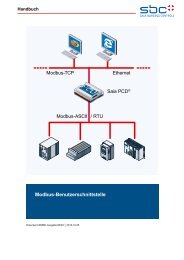
SAIA PCD - SBC-support
SAIA PCD - SBC-support
SAIA PCD - SBC-support

You also want an ePaper? Increase the reach of your titles
YUMPU automatically turns print PDFs into web optimized ePapers that Google loves.
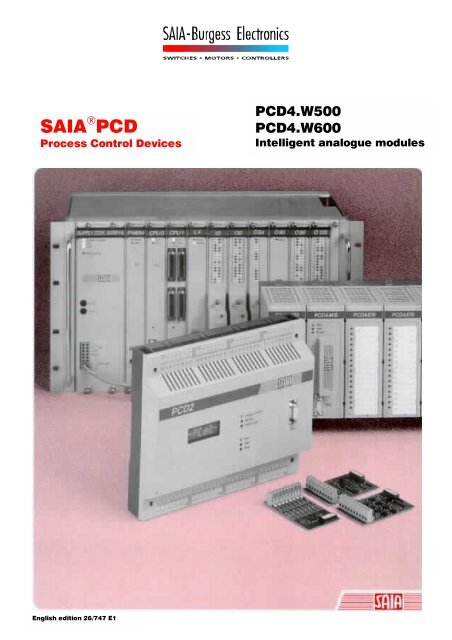
<strong>SAIA</strong> ® <strong>PCD</strong><br />
Process Control Devices<br />
<strong>PCD</strong>4.W500<br />
<strong>PCD</strong>4.W600<br />
Intelligent analogue modules<br />
English edition 26/747 E1
<strong>SAIA</strong>-Burgess Electronics Ltd.<br />
Bahnhofstrasse 18<br />
CH-3280 Murten (Switzerland)<br />
http;//www.saia-burgess.com<br />
BA: Electronic Controllers Telephone 026 / 672 72 72<br />
Telefax 026 / 672 74 99<br />
___________________________________________________________________________________________________________________________<br />
<strong>SAIA</strong>-Burgess Companies<br />
Switzerland<br />
<strong>SAIA</strong>-Burgess Electronics AG<br />
Freiburgstrasse 33<br />
CH-3280 Murten<br />
026 672 77 77, Fax 026 670 19 83<br />
France<br />
<strong>SAIA</strong>-Burgess Electronics Sàrl.<br />
10, Bld. Louise Michel<br />
F-92230 Gennevilliers<br />
01 46 88 07 70, Fax 01 46 88 07 99<br />
Germany<br />
<strong>SAIA</strong>-Burgess Electronics GmbH<br />
Daimlerstrasse 1k<br />
D-63303 Dreieich<br />
06103 89 060, Fax 06103 89 06 66<br />
Nederlands<br />
<strong>SAIA</strong>-Burgess Electronics B.V.<br />
Hanzeweg 12c<br />
NL-2803 MC Gouda<br />
0182 54 31 54, Fax 0182 54 31 51<br />
Austria<br />
<strong>SAIA</strong>-Burgess Electronics Ges.m.b.H.<br />
Schallmooser Hauptstrasse 38<br />
A-5020 Salzburg<br />
0662 88 49 10, Fax 0662 88 49 10 11<br />
Belgium<br />
<strong>SAIA</strong>-Burgess Electronics Belgium<br />
Avenue Roi Albert 1er, 50<br />
B-1780 Wemmel<br />
02 456 06 20, Fax 02 460 50 44<br />
Italy<br />
<strong>SAIA</strong>-Burgess Electronics S.r.l.<br />
Via Cadamosto 3<br />
I-20094 Corsico MI<br />
02 48 69 21, Fax 02 48 60 06 92<br />
Hungary<br />
<strong>SAIA</strong>-Burgess Electronics Automation Kft.<br />
Liget utca 1.<br />
H-2040 Budaörs<br />
23 501 170, Fax 23 501 180<br />
Representatives<br />
Great Britain<br />
Canham Controls Ltd.<br />
25 Fenlake Business Centre, Fengate<br />
Peterborough PE1 5BQ UK<br />
01733 89 44 89, Fax 01733 89 44 88<br />
Portugal<br />
INFOCONTROL Electronica e Automatismo LDA.<br />
Praceta Cesário Verde, No 10 s/cv, Massamá<br />
P-2745 Queluz<br />
21 430 08 24, Fax 21 430 08 04<br />
Denmark<br />
Malthe Winje Automation AS<br />
Håndværkerbyen 57 B<br />
DK-2670 Greve<br />
70 20 52 01, Fax 70 20 52 02<br />
Spain<br />
Tecnosistemas Medioambientales, S.L.<br />
Poligono Industrial El Cabril, 9<br />
E-28864 Ajalvir, Madrid<br />
91 884 47 93, Fax 91 884 40 72<br />
Norway<br />
Malthe Winje Automasjon AS<br />
Haukelivn 48<br />
N-1415 Oppegård<br />
66 99 61 00, Fax 66 99 61 01<br />
Czech<br />
Republic<br />
ICS Industrie Control Service, s.r.o.<br />
Modranská 43<br />
CZ-14700 Praha 4<br />
2 44 06 22 79, Fax 2 44 46 08 57<br />
Sweden<br />
Malthe Winje Automation AB<br />
Truckvägen 14A<br />
S-194 52 Upplands Våsby<br />
08 795 59 10, Fax 08 795 59 20<br />
Poland<br />
SABUR Ltd.<br />
ul. Druzynowa 3A<br />
PL-02-590 Warszawa<br />
22 844 63 70, Fax 22 844 75 20<br />
Suomi/<br />
Finland<br />
ENERGEL OY<br />
Atomitie 1<br />
FIN-00370 Helsinki<br />
09 586 2066, Fax 09 586 2046<br />
Australia<br />
Siemens Building Technologies Pty. Ltd.<br />
Landis & Staefa Division<br />
411 Ferntree Gully Road<br />
AUS-Mount Waverley, 3149 Victoria<br />
3 9544 2322, Fax 3 9543 8106<br />
Argentina<br />
MURTEN S.r.l.<br />
Av. del Libertador 184, 4° “A”<br />
RA-1001 Buenos Aires<br />
054 11 4312 0172, Fax 054 11 4312 0172<br />
After sales service<br />
USA<br />
<strong>SAIA</strong>-Burgess Electronics Inc.<br />
1335 Barclay Boulevard<br />
Buffalo Grove, IL 60089, USA<br />
847 215 96 00, Fax 847 215 96 06<br />
___________________________________________________________________________________________________________________________<br />
Issue : 22.11.2000<br />
Subjet to change without notice
<strong>SAIA</strong> ® Process Control Devices<br />
Intelligent analogue<br />
modules<br />
<strong>PCD</strong>4.W500 and <strong>PCD</strong>4.W600<br />
Supplement to “<strong>PCD</strong>4 Series - Hardware Manual” 26/734 E<br />
<strong>SAIA</strong>-Burgess Electronics Ltd. 1998. All rights reserved<br />
Edition 26/747 E1 - 08.1998<br />
Subject to technical changes<br />
© <strong>SAIA</strong>-Burgess Electronics Ltd.
Updates<br />
Manual : Intelligent analogue modules <strong>PCD</strong>4.W500 and <strong>PCD</strong>4.W600 - Edition E1<br />
Date Chapter Page Description<br />
© <strong>SAIA</strong>-Burgess Electronics Ltd.
<strong>PCD</strong>4.W500/W600<br />
Table of contents<br />
Table of contents<br />
Page<br />
1. <strong>PCD</strong>4.W500 Galvanically isolated, analogueinput<br />
module, 12/15-bit resolution<br />
1.1 Hardware and technical data 1-2<br />
1.1.1 Module overview 1-2<br />
1.1.2 Technical data 1-3<br />
1.1.3 Layout 1-4<br />
1.1.4 Insertion of range modules 1-5<br />
1.1.5 Block diagram 1-6<br />
1.1.6 Meaning of 16 addresses 1-7<br />
1.1.7 Module connections, taking into consideration<br />
the signal transmitter used 1-8<br />
1.2 Standard mode 1-13<br />
1.2.1 Software 1-13<br />
1.2.2 User program 1-14<br />
1.3 Extended mode with FB library 1-15<br />
1.3.1 Description of integrated functions 1-15<br />
1.3.2 Programming model 1-18<br />
1.3.3 Programming integrated functions 1-20<br />
1.3.4 FB description 1-23<br />
- RdValUp 1-24<br />
- RdValBp 1-25<br />
- RdStatus 1-26<br />
- Config 1-27<br />
- WrCData 1-29<br />
- RdCData 1-30<br />
- Control 1-31<br />
- RdInfo 1-32<br />
1.3.5 User program / Examples 1-33<br />
1.4 Extended mode with FBoxes in FUPLA 1-41<br />
1.4.1 The FBox '<strong>PCD</strong>4.W500' 1-41<br />
1.4.2 The FBox '<strong>PCD</strong>4.W5 Temp_3/4 wire' 1-45<br />
1.4.3 The FBox '<strong>PCD</strong>4.W5 Channel Status' 1-48<br />
26/747 E1 (W56-00-E.DOC) © <strong>SAIA</strong>-Burgess Electronics Ltd. Page 1
Table of contents<br />
<strong>PCD</strong>4.W500/W600<br />
Page<br />
2. <strong>PCD</strong>4.W600 Galvanically isolated analogue<br />
output module, 12-bit resolution<br />
2.1 Hardware and technical data 2-2<br />
2.1.1 Module overview 2-2<br />
2.1.2 Technical data 2-3<br />
2.1.3 Layout of the module 2-4<br />
2.1.4 Insertion of range modules 2-5<br />
2.1.5 Block diagram 2-6<br />
2.1.6 Meaning of the 16 addresses 2-7<br />
2.1.7 Module connections 2-8<br />
2.2 Standard mode 2-9<br />
2.2.1 Software 2-9<br />
2.2.2 User program to output an analogue value 2-10<br />
2.3 Extended mode with FB library 2-11<br />
2.3.1 Single Shot Mode 2-11<br />
2.3.2 Programming model 2-13<br />
2.3.3 Programming integrated functions 2-15<br />
2.3.4 FB description 2-17<br />
- WrVal 2-18<br />
- WrPreVal 2-19<br />
- RdStatus 2-20<br />
- Config 2-21<br />
- WrCData 2-23<br />
- RdCData 2-24<br />
- Control 2-25<br />
- RdInfo 2-26<br />
2.3.5 User program / Example 2-27<br />
2.4 Extended mode with FBoxes in FUPLA 2-31<br />
Page 2 © <strong>SAIA</strong>-Burgess Electronics Ltd. (W56-00-E.DOC) 26/747 E1
<strong>PCD</strong>4.W500/W600<br />
Table of contents<br />
Please note :<br />
A number of detailed manuals are available to aid installation and operation<br />
of the <strong>SAIA</strong> <strong>PCD</strong>. These are for use by technically qualified staff,<br />
who may also have successfully completed one of our "workshops".<br />
To obtain the best performance from your <strong>SAIA</strong> <strong>PCD</strong>, closely follow the<br />
guidelines for assembly, wiring, programming and commissioning given<br />
in these manuals. In this way, you will also become one of the many enthusiastic<br />
<strong>SAIA</strong> <strong>PCD</strong> users.<br />
If you have any technical suggestions or recommendations for improvements<br />
to the manuals, please let us know. A form is provided on the last<br />
page of this manual for your comments.<br />
Summary<br />
<strong>PCD</strong>1/2 series <strong>PCD</strong>4 series <strong>PCD</strong>6 series<br />
General<br />
Manuals<br />
Hardware<br />
<strong>PCD</strong>1<br />
<strong>PCD</strong>2<br />
Serie xx7<br />
<strong>PCD</strong>2.M220<br />
<strong>PCD</strong>2.H...<br />
Hardware<br />
<strong>PCD</strong>4<br />
W500/<br />
W600<br />
<strong>PCD</strong>4.H1..<br />
<strong>PCD</strong>4.H2..<br />
*)<br />
<strong>PCD</strong>4.H3..<br />
*)<br />
<strong>PCD</strong>4.H4..<br />
*)<br />
*)<br />
Hardware<br />
<strong>PCD</strong>6<br />
*) Adapter module 4'717'4828'0<br />
allows H modules to be used<br />
with the <strong>PCD</strong>6.<br />
User's<br />
Guide<br />
Reference<br />
Guide<br />
(P G3)<br />
<strong>PCD</strong>8.P1..<br />
PC D7.D1..<br />
PC A2.D1..<br />
PC D7.D2..<br />
- S-Bus<br />
- PROFIBUS<br />
- Remote I/O<br />
Installation<br />
Components<br />
for RS 485-<br />
Networks<br />
- PG4<br />
- Modem<br />
FUPLA/<br />
KOPLA<br />
function<br />
families<br />
26/747 E1 (W56-00-E.DOC) © <strong>SAIA</strong>-Burgess Electronics Ltd. Page 3
Table of contents<br />
<strong>PCD</strong>4.W500/W600<br />
Reliability and safety of electronic controllers<br />
<strong>SAIA</strong>-Burgess Electronics Ltd. is a company which devotes the greatest<br />
care to the design, development and manufacture of its products:<br />
• state-of-the-art technology<br />
• compliance with standards<br />
• ISO 9001 certification<br />
• international approvals: e.g. Germanischer Lloyd, UL,<br />
Det Norske Veritas, CE mark ...<br />
• choice of high-quality componentry<br />
• quality control checks at various stages of production<br />
• in-circuit tests<br />
• run-in (burn-in at 85°C for 48h)<br />
Despite every care, the excellent quality which results from this does<br />
have its limits. It is therefore necessary, for example, to reckon with the<br />
natural failure of components. For this reason <strong>SAIA</strong>-Burgess Electronics<br />
Ltd. provides a guarantee according to the "General terms and conditions<br />
of supply".<br />
The plant engineer must in turn also contribute his share to the reliable<br />
operation of an installation. He is therefore responsible for ensuring that<br />
controller use conforms to the technical data and that no excessive<br />
stresses are placed on it, e.g. with regard to temperature ranges, overvoltages<br />
and noise fields or mechanical stresses.<br />
In addition, the plant engineer is also responsible for ensuring that a<br />
faulty product in no case leads to personal injury or even death, nor to<br />
the damage or destruction of property. The relevant safety regulations<br />
should always be observed. Dangerous faults must be recognized by additional<br />
measures and any consequences prevented. For example, outputs<br />
which are important for safety should lead back to inputs and be monitored<br />
from software. Consistent use should be made of the diagnostic<br />
elements of the <strong>PCD</strong>, such as the watchdog, exception organization<br />
blocks (XOB) and test or diagnostic instructions.<br />
If all these points are taken into consideration, the <strong>SAIA</strong> <strong>PCD</strong> will provide<br />
you with a modern, safe programmable controller to control, regulate<br />
and monitor your installation with reliability for many years.<br />
Page 4 © <strong>SAIA</strong>-Burgess Electronics Ltd. (W56-00-E.DOC) 26/747 E1
<strong>PCD</strong>4.W500<br />
Analogue Input Module 12 bit<br />
1. <strong>PCD</strong>4.W500 Galvanically isolated, analogue<br />
input module, 12/15-bit resolution<br />
Intelligent analogue input module with galvanic isolation, 12/15-bit resolution<br />
and A/D conversion time of 100 µs (single shot). As a range<br />
module it is used with <strong>PCD</strong>7.Wlxx modules. The following connections<br />
are therefore possible:<br />
• 8 inputs for voltages 0..+10 V<br />
• 8 inputs for currents 0..20 mA<br />
• 8 inputs for Pt/Ni 1000 resistance thermometers, 2 wire<br />
• 4 inputs for Pt 100/1000 or Ni 100/1000 resistance thermometers,<br />
4 wire<br />
A microcontroller enables intelligent functions to be executed locally<br />
without burdening the central processor module:<br />
• single-shot - continuous measurement<br />
• formats: - 12 bit (single shot) - 12/15 bit (continuous),<br />
- proportional to input size<br />
- user definable scaling<br />
• comparator function with two limiting values per input and adjustable<br />
hysteresis<br />
• linearization and conversion to °C when standard temperature sensors<br />
are used<br />
• connection of resistance thermometers (Pt 100/1000, Ni 100/100)<br />
• status information, such as wire break, short-circuit or error<br />
26/747 E1 (D4W5-1-E.DOC) © <strong>SAIA</strong>-Burgess Electronics Ltd. Page 1-1
Analogue Input Module 12 bit<br />
<strong>PCD</strong>4.W500<br />
1.1 Hardware and technical data<br />
1.1.1 Module overview<br />
Base module:<br />
<strong>PCD</strong>4.W500<br />
containing the galvanically isolated DC/DC converter to<br />
supply the plug-in range modules, the input multiplexer,<br />
A/D converter, programmable current source, optocoupler<br />
for galvanic isolation from the <strong>PCD</strong> processor,<br />
microcontroller with its peripheral components, such as<br />
the I/O bus interface.<br />
Range modules:<br />
<strong>PCD</strong>7.W100<br />
4 channels, ranges 0..10 V / ±10 V<br />
<strong>PCD</strong>7.W101 4 channels, ranges 0..1 V / ±1 V (4 wire Ni/Pt 100/1000)<br />
<strong>PCD</strong>7.W103 4 channels, range 0..20 mA (4..20 mA)<br />
<strong>PCD</strong>7.W104 4 channels, range 4 .. 20 mA for 2 wire measuring transducer<br />
<strong>PCD</strong>7.W110 4 channels for Pt 1000, range -50 .. +150°C, 2-wire<br />
measurement<br />
<strong>PCD</strong>7.W111 4 channels for Ni 1000, range -50 .. +150°C, 2-wire<br />
measurement<br />
<strong>PCD</strong>7.W120 4 channels for Pt/Ni 100/1000 constant current outputs<br />
The input filter time constant is 1 ms<br />
Page 1-2 © <strong>SAIA</strong>-Burgess Electronics Ltd. (D4W5-1-E.DOC) 26/747 E1
<strong>PCD</strong>4.W500<br />
Analogue Input Module 12 bit<br />
1.1.2 Technical data (base module)<br />
Total inputs per module<br />
Potential isolation<br />
Input measurement principle<br />
Signal range<br />
Digital display<br />
(resolution)<br />
8 voltage or current inputs or<br />
8/4 inputs for resistance thermometers<br />
(Pt 100/1000 or Ni 100/1000)<br />
Yes, between <strong>PCD</strong>-GND and module<br />
GND 500 VDC, 1 min<br />
Differential<br />
See range modules<br />
12 bit (0 .. 4095), single-shot mode<br />
A/D conversion time max. 100 µs single shot<br />
max. 65 µs continous<br />
Admissible over-voltage at<br />
analogue inputs<br />
Accuracy regarding<br />
range end value<br />
Repeating accuracy<br />
Temperature error<br />
Current outputs<br />
60 VDC<br />
± 0.25% ± 2 LSB<br />
± 2 LSB<br />
± 0.02% /°C<br />
0 .. 10 mA constant current for resistance<br />
sensors (for use with <strong>PCD</strong>7.W120 range<br />
module only).<br />
Standard value 2 mA. Resolution: 8 bit<br />
Resistance to interference 2 kV in capacitive coupling<br />
(burst)<br />
with screening<br />
Common-mode behaviour U IN + U CM ≤ ± 10 V CMR > 75 dB<br />
+<br />
U<br />
IN<br />
-<br />
+<br />
-<br />
U CM<br />
Filter<br />
PGND<br />
CM: Common Mode<br />
External supply 24 VDC<br />
Current consumption<br />
as <strong>PCD</strong>4.N21 (transformer 19 V, bridge<br />
rectifier)<br />
internal from <strong>PCD</strong>4 bus +5 V: 150 mA<br />
external for current output +24 V: 100 mA<br />
26/747 E1 (D4W5-1-E.DOC) © <strong>SAIA</strong>-Burgess Electronics Ltd. Page 1-3
Analogue Input Module 12 bit<br />
<strong>PCD</strong>4.W500<br />
1.1.3 Layout<br />
µC<br />
Microcontroller<br />
Bus connector<br />
I/O bus decoder<br />
LED OK<br />
Supply, galv. isolated<br />
4 optocouplers<br />
A/D converter<br />
<strong>PCD</strong>4.W50<br />
Bipolar<br />
Unipolar<br />
Gain<br />
Offset<br />
B<br />
A<br />
NOT<br />
ISOL.<br />
ISOL.<br />
SUPPLY<br />
4 ... 7<br />
0 ... 3<br />
Jumper, Supply isol. - not isol.<br />
Offset pot.<br />
Jumper bipolar- unipolar<br />
Measuring range module B<br />
Multiplexers<br />
Measuring range module A<br />
Connector to terminals<br />
Amplification pot (gain)<br />
The following functional blocks can be seen:<br />
• Basic card with bus interface, address decoding, microcontroller system,<br />
optocouplers, multiplexers and two spaces for insertion of range<br />
modules.<br />
• Space A for insertion of range module with addresses 0 .. 3 and space<br />
B for insertion of range module with addresses 4 .. 7.<br />
The "Offset" and "Gain" potentiometers are pre-set in the factory and<br />
should not be adjusted.<br />
Page 1-4 © <strong>SAIA</strong>-Burgess Electronics Ltd. (D4W5-1-E.DOC) 26/747 E1
<strong>PCD</strong>4.W500<br />
Analogue Input Module 12 bit<br />
1.1.4 Insertion of range modules<br />
To plug on a range module, the printed circuit board must be removed<br />
from the module's housing. This is done by pressing in the snap-latches<br />
either side of the front cover. The screw fastening for the card, located on<br />
the left side of the module at the top, should then be unscrewed, allowing<br />
the printed circuit board to be pulled out of the housing.<br />
In space A, the lower position, a range module can be inserted for 4<br />
channels with addresses 0 ... 3. Space B, the upper position, is intended<br />
for the 4 channels with addresses 4 ... 7, or for the special module<br />
<strong>PCD</strong>7.W120 (resistance thermometers, etc.).<br />
After inserting the range modules, the housing should be closed again and<br />
the screw fastening for the card replaced.<br />
Caution:<br />
The basic card and range modules all contain components<br />
which are sensitive to electrostatic discharges.<br />
Various range modules can be inserted in spaces A and B. In order that<br />
this equipment can be identified externally at any time, remember to enter<br />
details on the front and side panel plates.<br />
0 .. 10V Pt 1000<br />
26/747 E1 (D4W5-1-E.DOC) © <strong>SAIA</strong>-Burgess Electronics Ltd. Page 1-5
Analogue Input Module 12 bit<br />
<strong>PCD</strong>4.W500<br />
1.1.5 Block diagram<br />
EEPROM<br />
Microcontroller<br />
I/O bus interface<br />
<strong>PCD</strong>4 bus<br />
galvanic<br />
Optocoupler<br />
isolation<br />
Input<br />
Range<br />
Module A<br />
Input<br />
Range<br />
Module B<br />
MUX<br />
U<br />
B<br />
Jumper<br />
A D<br />
Ref<br />
Current<br />
Source<br />
0..10 mA<br />
GND<br />
+24V<br />
DC-DC<br />
converter<br />
± 15V, +5V<br />
*) 47 nF *)<br />
250V<br />
Isol. Not Isol<br />
Supply<br />
Jumper<br />
AGND<br />
*) To carry out an isolation test (500 VDC) on the installation, the<br />
screening components on the <strong>PCD</strong>4.C2.. must be removed.<br />
Page 1-6 © <strong>SAIA</strong>-Burgess Electronics Ltd. (D4W5-1-E.DOC) 26/747 E1
<strong>PCD</strong>4.W500<br />
Analogue Input Module 12 bit<br />
1.1.6 Meaning of the 16 addresses<br />
I/O address:<br />
0 1 2 3 4 5 6 7 8 9 10 11 12 13 14 15<br />
Write (outputs)<br />
Channel address<br />
Data address<br />
Read (inputs)<br />
C0 C1 C2 C3 C4 C5 C6 C7<br />
Conv Status Write<br />
O0 O1 O2 O3<br />
D0 D1 D2 D3 D4 D5 D6 D7 D8 D9 D10 D11 D12 D13 D14<br />
Data<br />
'0'<br />
Data<br />
'1'<br />
D0 D1 D2 D3 D4 D5 D6 D7 D8 D9 D10 D11 D12 D13 D14 Busy<br />
LSB<br />
C0 .. C7: Channel selection SET O Kx<br />
Conv: SET/RES O 8 starts conversion (data input/output) *)<br />
Status: SET/RES O 9 gives the status register at D0 .. D14 *)<br />
Write: Write/read<br />
O0..3: 4-bit address<br />
Data: Selects data or channel address<br />
D0..D14: 15-bit data → Conv<br />
Status register → Status<br />
*) Busy "Input" = H<br />
26/747 E1 (D4W5-1-E.DOC) © <strong>SAIA</strong>-Burgess Electronics Ltd. Page 1-7
Analogue Input Module 12 bit<br />
<strong>PCD</strong>4.W500<br />
1.1.7 Module connections, taking into consideration the signal<br />
transmitter used<br />
Voltage inputs for ranges 0..10 V / ±10 V, 0..1 V / ±1 V<br />
µC<br />
Range module<br />
A<br />
Range module<br />
B<br />
Bipolar<br />
Unipolar<br />
Offset<br />
B<br />
NOT<br />
ISOL.<br />
IS OL.<br />
SUPPLY<br />
4 ... 7<br />
4 inputs<br />
I4 ... I7<br />
4 inputs<br />
I0 ... I3<br />
1 3 5 7 9 11 13 15<br />
0 2 4 6 8 10 12 14 _<br />
_ +<br />
_ +<br />
_ +<br />
_ +<br />
_<br />
+<br />
_<br />
+<br />
_<br />
+<br />
_<br />
+<br />
I 0 I 1 I 2 I 3 I 4 I 5 I 6 I 7<br />
+<br />
b<br />
+24V<br />
a<br />
Gain<br />
A<br />
0 ... 3<br />
Range module <strong>PCD</strong>7.W100 0..10 V → 0..4095: unipolar<br />
± 10 V → 0..4095: bipolar<br />
Range module <strong>PCD</strong>7.W101: 0..1 V → 0..4095: unipolar<br />
± 1 V → 0..4095: bipolar<br />
Module spaces A and B can be equipped with different range modules.<br />
500V*)<br />
U<br />
+<br />
-<br />
W100/101<br />
+<br />
-<br />
A<br />
D<br />
+<br />
24V<br />
500V*)<br />
24V<br />
- ±==15V<br />
Supply<br />
±==10V**)<br />
AGND<br />
BIPOLAR<br />
UNIPOLAR<br />
<strong>PCD</strong>4-GND<br />
Not Isol.<br />
Isol.<br />
*) Isolation voltage of galvanic isolation<br />
**) Common mode voltage<br />
Page 1-8 © <strong>SAIA</strong>-Burgess Electronics Ltd. (D4W5-1-E.DOC) 26/747 E1
<strong>PCD</strong>4.W500<br />
Analogue Input Module 12 bit<br />
Current inputs for ranges 0..20 mA and 4 ... 20 mA<br />
µC<br />
Range module<br />
A<br />
Range module<br />
B<br />
Bipolar<br />
Unipolar<br />
Offset<br />
B<br />
NOT<br />
ISOL.<br />
IS OL.<br />
SUPPLY<br />
4 ... 7<br />
4 inputs<br />
I4 ... I7<br />
4 inputs<br />
I0 ... I3<br />
1 3 5 7 9 11 13 15<br />
0 2 4 6 8 10 12 14 _<br />
_ +<br />
_ +<br />
_ +<br />
_ +<br />
_<br />
+<br />
_<br />
+<br />
_<br />
+<br />
_<br />
+<br />
I 0 I 1 I 2 I 3 I 4 I 5 I 6 I 7<br />
+<br />
b<br />
+24V<br />
a<br />
Gain<br />
A<br />
0 ... 3<br />
Range module <strong>PCD</strong>7.W103: measuring range 0..20 mA → 0..4095<br />
For range 4 ... 20 mA, the same range module is used. Current limits are<br />
monitored with the user program. The jumper should be in the<br />
UNIPOLAR position.<br />
4 mA = 819 digital measurement<br />
20 mA = 4095 digital measurement<br />
Module spaces A and B can be equipped with different range modules<br />
(e.g. A: 0..20 mA, B: ±10 V).<br />
W103<br />
500V*)<br />
I<br />
49.9Ω<br />
+<br />
-<br />
A<br />
D<br />
+<br />
24V<br />
500V*)<br />
24V<br />
- ±==15V<br />
Supply<br />
±==10V**)<br />
AGND<br />
BIPOLAR<br />
UNIPOLAR<br />
<strong>PCD</strong>4-GND<br />
Not Isol.<br />
Isol.<br />
*) Isolation voltage of galvanic isolation<br />
**) Common mode voltage<br />
26/747 E1 (D4W5-1-E.DOC) © <strong>SAIA</strong>-Burgess Electronics Ltd. Page 1-9
Analogue Input Module 12 bit<br />
<strong>PCD</strong>4.W500<br />
Current inputs for 4 ... 20 mA from two-wire measuring transducer<br />
Two-wire measuring transducers need a 24 VDC supply on the instrument<br />
line, as shown in the diagram below.<br />
µC<br />
Range module<br />
A<br />
Range module<br />
B<br />
Bipolar<br />
Unipolar<br />
Offset<br />
B<br />
NOT<br />
ISOL.<br />
IS OL.<br />
SUPPLY<br />
4 ... 7<br />
4 inputs<br />
I4 ... I7<br />
4 inputs<br />
I0 ... I3<br />
1 3 5 7 9 11 13 15<br />
0 2 4 6 8 10 12 14 _<br />
_ +<br />
_ +<br />
_ +<br />
_ +<br />
_<br />
+<br />
_<br />
+<br />
_<br />
+<br />
_<br />
+<br />
I 0 I 1 I 2 I 3 I 4 I 5 I 6 I 7<br />
+<br />
b<br />
+24V<br />
a<br />
Gain<br />
A<br />
0 ... 3<br />
Range module <strong>PCD</strong>7.W104: measuring range 4 ... 20 mA<br />
4 mA = 819 digital measurement<br />
20 mA = 4095 digital measurement<br />
The SUPPLY jumper must be set to NOT ISOL.<br />
A voltage of + 24 VDC must be applied at the + terminal to supply the<br />
measuring transducer. The demands on this voltage are the same as for<br />
the <strong>PCD</strong>4.N2.. power supply module, or as specified by the transducer<br />
manufacturer. Maximum current requirement 0.2 A when 8 measuring<br />
transducers are connected.<br />
Module spaces A and B can be equipped with different range modules<br />
(e.g. A: 4 ... 20 mA, B: ±10 V).<br />
MU<br />
4..20mA<br />
W104<br />
500V**)<br />
*) Same potential<br />
of 24V and<br />
transducer<br />
**) Isolation<br />
voltage of<br />
galvanic<br />
isolation<br />
-<br />
+<br />
24V<br />
PTC<br />
49,9Ω<br />
0V*)<br />
24V<br />
- ±==15V<br />
Supply<br />
Not Isol. Isol.<br />
+<br />
-<br />
AGND<br />
BIPOLAR<br />
UNIPOLAR<br />
A<br />
D<br />
<strong>PCD</strong>4-GND<br />
Page 1-10 © <strong>SAIA</strong>-Burgess Electronics Ltd. (D4W5-1-E.DOC) 26/747 E1
<strong>PCD</strong>4.W500<br />
Analogue Input Module 12 bit<br />
Connection of 4 x Pt 100/1000 or Ni 100/1000 resistance<br />
thermometers (4-wire measurement)<br />
µC<br />
Range module Range module<br />
A<br />
B<br />
4 inputs 4 current outputs<br />
1 3 5 7 9 11 13 15<br />
0 2 4 6 8 10 12 14<br />
+<br />
b<br />
a<br />
Bipolar<br />
Unipolar<br />
Offset<br />
B<br />
NOT<br />
ISOL.<br />
IS OL.<br />
SUPPLY<br />
4 ... 7<br />
4 outputs<br />
O0 ... O3<br />
4 inputs<br />
I0 ... I3<br />
+ + + +<br />
I 0 I 1 I 2 I 3<br />
+ + + +<br />
O 4 O 5 O 6 O 7<br />
+24V<br />
Gain<br />
A<br />
0 ... 3<br />
Range module space A:<br />
<strong>PCD</strong>7.W101 (0..1 V)<br />
Range module space B:<br />
<strong>PCD</strong>7.W120<br />
for 4 constant current outputs 0..10 mA<br />
The jumper must be set to the UNIPOLAR position.<br />
The module in space B provides a constant current of 0..10 mA, 8 bit.<br />
The potential drop at resistance thermometers is channelled to the voltage<br />
range module in space A.<br />
Important: unused current outputs must be short-circuited.<br />
W120 + W 101<br />
500V*)<br />
Ni/Pt<br />
100/<br />
1000 ϑ<br />
I<br />
+<br />
-<br />
A<br />
D<br />
BIPOLAR<br />
UNIPOLAR<br />
500V*)<br />
+<br />
24V<br />
24V<br />
- ±==15V<br />
<strong>PCD</strong>4-GND<br />
*) Isolation voltage<br />
of galvanic isolation<br />
Not Isol.<br />
Supply<br />
Isol.<br />
AGND<br />
26/747 E1 (D4W5-1-E.DOC) © <strong>SAIA</strong>-Burgess Electronics Ltd. Page 1-11
Analogue Input Module 12 bit<br />
<strong>PCD</strong>4.W500<br />
Module connection of 8 x Pt 1000, Ni 1000 resistance thermometers<br />
(2-wire measurement) for temperature range -50 ... +150°C<br />
µC<br />
Range module<br />
A<br />
Range module<br />
B<br />
Bipolar<br />
Unipolar<br />
Offset<br />
B<br />
NOT<br />
ISOL.<br />
IS OL.<br />
SUPPLY<br />
4 ... 7<br />
4 inputs<br />
I4 ... I7<br />
4 inputs<br />
I0 ... I3<br />
1 3 5 7 9 11 13 15<br />
0 2 4 6 8 10 12 14 _<br />
_ +<br />
_ +<br />
_ +<br />
_ _ _ + + +<br />
_<br />
+<br />
_<br />
+<br />
I 0 I 1 I 2 I 3 I 4 I 5 I 6 I 7<br />
+<br />
b<br />
+24V<br />
a<br />
Gain<br />
A<br />
0 ... 3<br />
Range module <strong>PCD</strong>7.W110 for 4 x Pt 1000 (-50 .. +150°C)<br />
<strong>PCD</strong>7.W111 for 4 x Ni 1000 (-50 .. +150°C)<br />
At each of these modules, 4 x Pt/Ni 1000 resistance thermometers can be<br />
connected. Supply voltages for the resistance thermometers provide a<br />
stabilized internal supply for the module. Modules have been adjusted in<br />
the factory and are independent of the <strong>PCD</strong>4.W500 base module, i.e.<br />
modules are interchangeable.<br />
Adjustment to compensate for cable length can be made for each channel<br />
by means of the potentiometers on the module itself. To maintain interchangeability,<br />
however, it is preferable to compensate in the user<br />
program.<br />
Important: Unused inputs must be short-circuited.<br />
500V*)<br />
Pt/Ni<br />
1000<br />
+<br />
-<br />
W110/111<br />
+<br />
-<br />
A<br />
D<br />
500V*)<br />
BIPOLAR<br />
UNIPOLAR<br />
+<br />
24V<br />
24V<br />
- ±==15V<br />
Supply<br />
AGND<br />
<strong>PCD</strong>4-GND<br />
Not Isol.<br />
Isol.<br />
*) Isolation voltage of galvanic isolation<br />
Page 1-12 © <strong>SAIA</strong>-Burgess Electronics Ltd. (D4W5-1-E.DOC) 26/747 E1
<strong>PCD</strong>4.W500<br />
Analogue Input Module 12 bit<br />
1.2 Standard mode<br />
1.2.1 Software<br />
If the microcontroller (µC) is left unconfigured, the <strong>PCD</strong>4.W500 module<br />
is treated like the <strong>PCD</strong>4.W300. However, the module (µC) can be configured<br />
in such a way that measured results are directly available in °C.<br />
See the following chapters 1.3 and 1.4 "Extended modes".<br />
Important note:<br />
If the module has been used previously in 'continuous'<br />
mode, this configuration is stored in the EEPROM. On<br />
the next startup, this configuration is taken again and the<br />
'single shot' mode will therefore no longer work. The<br />
EEPROM must be reconfigured first.<br />
Solution:<br />
Programming with FBoxes: A simple user program with<br />
the FBox '<strong>PCD</strong>4W500' with all channels set as 'disabled'<br />
is to create and to run.<br />
Programming with FB's: In the Config-DB column 'Conf',<br />
for all channels the code 0000H is to fill in, then the user<br />
program is to run. Program example 1, 'example1.src' can<br />
be used, see chapter 1.3.5).<br />
26/747 E1 (D4W5-1-E.DOC) © <strong>SAIA</strong>-Burgess Electronics Ltd. Page 1-13
Analogue Input Module 12 bit<br />
<strong>PCD</strong>4.W500<br />
1.2.2 User program for single-shot inquiry<br />
Example in IL (Instruction List) to demonstrate principle, with wait loop to<br />
await "Busy".<br />
Convert the analogue value at input 3 (channel 3) and save it in register<br />
R 103. The module has base address 32.<br />
BA EQU O 32<br />
(ACC H) ; The ACCU must be high<br />
RES BA+15 ; Output 15 must be low<br />
SET BA+3 ; Selection of channel 3<br />
(RES BA+8)<br />
SET BA+8 ; Start A/D conversion by switching<br />
RES BA+8 ; output 8 on and off.<br />
busy: STH BA+15 ; Busy is high when conversion running.<br />
JR H busy ; Wait for as long as busy is high.<br />
BITI 12 ; Read the 12 bits from<br />
BA+0 ; address 0<br />
R 103 ; and write to register R 103<br />
Since the reading of an analogue value is a sequential process, it is preferable<br />
to write the user program in GRAFTEC (no program jumps, no<br />
wait loops).<br />
1<br />
Execute channel<br />
selection and conversion<br />
RES<br />
SET<br />
SET<br />
RES<br />
BA+15<br />
BA+3<br />
BA+8<br />
BA+8<br />
1<br />
Busy abwarten<br />
STL<br />
BA+15<br />
2<br />
Wert --> R 103<br />
BITI 12<br />
BA+0<br />
R 103<br />
Page 1-14 © <strong>SAIA</strong>-Burgess Electronics Ltd. (D4W5-1-E.DOC) 26/747 E1
<strong>PCD</strong>4.W500<br />
Analogue Input Module 12 bit<br />
1.3 Extended mode with FB library<br />
1.3.1 Description of integrated functions<br />
Standard / Single Shot mode<br />
(Factory configuration without additional programming)<br />
Value in 12-bit format (0..4095)<br />
Converted each time the value is queried.<br />
Conversion time: 100 µs<br />
Continuous mode (voltage , current, temperature resistance mode)<br />
In this mode, inputs are converted continuously in a cycle and the value<br />
is stored in memory. When the value is queried, the current value is read<br />
directly from memory.<br />
Conversion time : 65 µs (time taken for value to be ready for reading)<br />
Currency of voltage, current: - low resolution: 2 ms<br />
values: - high resolution: 160 ms *)<br />
temperature - 2 wire connection: 160 ms *)<br />
- 4 wire connection: 100 ms<br />
per channel *)<br />
(max. 400 ms with 4 channels)<br />
*) 50/60 Hz suppression<br />
Voltage, current mode<br />
The following formats can be selected for measurement of voltage and<br />
current:<br />
• Bit format:<br />
Digital representation 12 bit 0..4095 (low resolution)<br />
or 15 bit 0..32767 (high resolution)<br />
• Proportional format:<br />
Digitale representation in physical values<br />
Voltage range:<br />
10 V → 1 bit = 1 mV, representation 0..10000 / ±10000<br />
1 V → 1 bit = 100 µV, representation 0..10000 / ±10000<br />
Current range:<br />
20 mA → 1 bit = 1 µA, representation 0..20000<br />
Resolution:<br />
at low resolution, steps of 10/5: 0, 10, 20,… (current 0, 5, 10,…)<br />
at high resolution, single steps 0, 1, 2..<br />
26/747 E1 (D4W5-1-E.DOC) © <strong>SAIA</strong>-Burgess Electronics Ltd. Page 1-15
Analogue Input Module 12 bit<br />
<strong>PCD</strong>4.W500<br />
• User Scaling<br />
In addition, a user definable scaling can be selected. By means of two<br />
15-bit values, the range and offset of the scale are specified for each<br />
channel.<br />
Range: 0..32767 (15 bit unsigned)<br />
Offset: -16384..+16383 (15 bit signed, 2's complement)<br />
Example: voltage input 0..10 V:<br />
Range: 4000<br />
Offset: -1000 (does not need to be symmetrical)<br />
Remark:<br />
e.g.: Offset < 0<br />
a) Offset ≥ 0: The total of offset+range must<br />
always be within 0..32767 (15 bit unsigned<br />
format). If not, the scaling error flag is set<br />
in the status register. The value is read with<br />
FB "RdValUpW5".<br />
16383<br />
3000<br />
b) Offset < 0: The total of offset+range must<br />
always be within -16384..+16383 (15 bit<br />
signed format). If not, the scaling error flag<br />
is set in the status register. The value is<br />
read with FB "RdValBpW5".<br />
Range<br />
4000<br />
Offset:<br />
0<br />
-1000<br />
-16384<br />
0<br />
10 Uin [V]<br />
Temperature resistance mode<br />
For temperature measurement, the linearisation and conversion to 0,1°C<br />
is pre-programmed for Ni/Pt 100/1000 temperature resistors.<br />
Digital representation : - range -50..150°C: -500..1500<br />
- range 0..600°C: 0..6000<br />
Page 1-16 © <strong>SAIA</strong>-Burgess Electronics Ltd. (D4W5-1-E.DOC) 26/747 E1
<strong>PCD</strong>4.W500<br />
Analogue Input Module 12 bit<br />
Comparator<br />
For each channel, two x 15-bit limiting values with adjustable hysteresis<br />
(8 bit / 0..255) can be entered.<br />
The value read back corresponds to several status bits, which show<br />
whether the actual value lies within these limits. This relieves the <strong>PCD</strong> of<br />
CMP commands with constants or registers. The analogue input functions<br />
as an adjustable threshold value switch. Setting 2 limiting values produces<br />
a window comparator.<br />
Hysterese B<br />
Comparator B<br />
Hysterese A<br />
Comparator A<br />
Value<br />
Value greater A<br />
Value greater B<br />
Value A Exor B<br />
Note: A hysteresis of 100 produces a comparator value of ± 50.<br />
Values can be read from the status register.<br />
The comparator limits must always be within the format<br />
range.<br />
26/747 E1 (D4W5-1-E.DOC) © <strong>SAIA</strong>-Burgess Electronics Ltd. Page 1-17
Analogue Input Module 12 bit<br />
<strong>PCD</strong>4.W500<br />
1.3.2 Programming model<br />
Mapping <strong>PCD</strong>4 adresses<br />
I/O 0 1 2 3 4 5 6 7 8 9 10 11 12 13 14 15<br />
For writing (Outputs)<br />
Channel/<br />
Address<br />
C0 C1 C2 C3 C4 C5 C6 C7 Conv<br />
*<br />
Status<br />
*<br />
Write A0 A1 A2 A3 Data<br />
‘0’<br />
Data D0 D1 D2 D3 D4 D5 D6 D7 D8 D9 D10 D11 D12 D13 D14 Data<br />
‘1’<br />
For reading (Inputs)<br />
D0 D1 D2 D3 D4 D5 D6 D7 D8 D9 D10 D11 D12 D13 D14 Busy<br />
C0..C7: Channel selection SET O Cx<br />
Conv: SET/RES O 8 starts conversion (Data input/output)* Interrupt 0<br />
Status: SET/RES O 9 gives the status register at D0..D14* Interrupt 1<br />
Write: Write / read<br />
A0..3: 4-bit address<br />
Data: Selects data or channel/address<br />
D0..D14: 15-bit data → Conv<br />
Status register → Status<br />
- The busy input is =1<br />
- Written data are evaluated by the microcontroller<br />
See chapter 1.2.2 for program example in IL and GRAFTEC.<br />
Page 1-18 © <strong>SAIA</strong>-Burgess Electronics Ltd. (D4W5-1-E.DOC) 26/747 E1
<strong>PCD</strong>4.W500<br />
Analogue Input Module 12 bit<br />
Status register<br />
Data Function<br />
D0 0: Value not greater than A<br />
1: Value greater than A<br />
D1 0: Value not greater than B<br />
1: Value greater than B<br />
D2 Logical result of A EXOR B<br />
D3 Scaling error<br />
D4, D5 not used<br />
D6 Wiring error<br />
D7 Channel error<br />
D8 - D10 Internal Error 3 bits : 000: everything ok<br />
001: CPU or internal RAM error<br />
010: external RAM error<br />
011: EPROM checksum error<br />
100: EEPROM checksum error<br />
101: EEPROM initi. or test error<br />
110: AD - converter error<br />
111: Watch dog error<br />
D11 not used<br />
D12 Suppression : 0: 50 Hz<br />
1: 60 Hz<br />
D13 Switch position : 0: unipolar<br />
1: bipolar<br />
D14 General error<br />
Explanation of error flags:<br />
Scaling error:<br />
Wiring error:<br />
Scaling is not possible.<br />
A short-circuit or wire break was detected during temperature<br />
measurement.<br />
Channel error: Set when the scaling or wiring error flag is set.<br />
Internal error:<br />
Controller system or peripheral device error.<br />
General error: Set if one of the above error flags is set.<br />
The easiest way to read the status register is using FB "RdStatus".<br />
26/747 E1 (D4W5-1-E.DOC) © <strong>SAIA</strong>-Burgess Electronics Ltd. Page 1-19
Analogue Input Module 12 bit<br />
<strong>PCD</strong>4.W500<br />
1.3.3 Programming integrated functions<br />
Individual parameters can be selected by their addresses:<br />
Address Meaning No. of bits<br />
01 Channel specific configuration 15 bit<br />
02 Value comparator A 15 bit<br />
03 Hysteresis comparator A 8 bit<br />
04 Value comparator B 15 bit<br />
05 Hysteresis comparator B 8 bit<br />
06 Current source value 8 bit<br />
07 User range scaling value 15 bit<br />
08 User range offset value 15 bit<br />
Table 1:Meaning of addresses<br />
Channel-specific configuration (address = 01)<br />
The programming default is single shot mode (FW default)<br />
Mode<br />
Single shot mode<br />
Range<br />
module<br />
Range Format Digital<br />
representation<br />
Configuration<br />
value<br />
Comparator<br />
off on<br />
Single shot - - - - 0000H -<br />
Table 2: Channel-specific configuration - single shot mode<br />
Single shot mode is programmed in the factory.<br />
Important:<br />
Not used channels must be configured as "single shot".<br />
Page 1-20 © <strong>SAIA</strong>-Burgess Electronics Ltd. (D4W5-1-E.DOC) 26/747 E1
<strong>PCD</strong>4.W500<br />
Analogue Input Module 12 bit<br />
Continuous mode<br />
a) low resolution<br />
Mode Equipped module Range Format Digital Configuration value<br />
representation<br />
Comparator<br />
off on<br />
Voltage <strong>PCD</strong>7.W100 10 V Bitformat 0..4095 0001H 0041H<br />
Proportional 0/-10000*/**..10000 0009H 0049H<br />
user scaling see user scaling** 0019H 0059H<br />
<strong>PCD</strong>7.W101 1 V Bitformat 0..4095 0081H 00C1H<br />
Proportional 0/-10000*/**..10000 0089H 00C9H<br />
user scaling see user scaling** 0099H 00D9H<br />
Current <strong>PCD</strong>7.W103 20 mA Bitformat 0..4095 0002H 0042H<br />
Proportional 0..20000 000AH 004AH<br />
user scaling see user scaling** 001AH 005AH<br />
<strong>PCD</strong>7.W104 4..20 mA Bitformat 0..4095 0082H 00C2H<br />
Proportional 0..20000 008AH 00CAH<br />
user scaling see user scaling** 009AH 00DAH<br />
Tabelle 3: Channel-specific configuration - low resolution<br />
b) high resolution with 50/60 Hz suppression<br />
Mode Equipped module Range Format Digital Configuration value<br />
representation Comparator<br />
off on<br />
Voltage <strong>PCD</strong>7.W100 10 V Bitformat 0..32767 0021H 0061H<br />
Proportional 0/-10000*/**..10000 0029H 0069H<br />
user scaling see user scaling** 0039H 0079H<br />
<strong>PCD</strong>7.W101 1 V Bitformat 0..32767 00A1H 00E1H<br />
Proportional 0/-10000*/**..10000 00A9H 00E9H<br />
user scaling see user scaling** 00B9H 00F9H<br />
Current <strong>PCD</strong>7.W103 20 mA Bitformat 0..32767 0022H 0062H<br />
Proportional 0..20000 002AH 006AH<br />
user scaling see user scaling** 003AH 007AH<br />
<strong>PCD</strong>7.W104 4..20 mA Bitformat 0..32767 00A2H 00E2H<br />
Proportional 0..20000 00AAH 00EAH<br />
user scaling see user scaling** 00BAH 00FAH<br />
Temperature <strong>PCD</strong>7.W110 Pt 1000 -50..150°C -500.1500** 082BH 086BH<br />
2 - wire connection<br />
<strong>PCD</strong>7.W111 Ni 1000 -50..150°C -500.1500** 0C2BH 0C6BH<br />
3 - wire connection<br />
<strong>PCD</strong>7.W101 Pt 100 -50..150°C -500.1500** 012BH 016BH<br />
+ <strong>PCD</strong>7.W12x Pt 100 0..600°C 0..6000 212BH 216BH<br />
(in preparation) Pt 1000 -50..150°C -500.1500** 092BH 096BH<br />
Pt 1000 0..600°C 0..6000 292BH 296BH<br />
Ni 100 -50..150°C -500.1500** 052BH 056BH<br />
Ni 1000 -50..150°C -500.1500** 0D2BH 0D6BH<br />
4 - wire connection<br />
<strong>PCD</strong>7.W101 Pt 100 -50..150°C -500.1500** 00ABH 00EBH<br />
+ <strong>PCD</strong>7.W120 Pt 100 0..600°C 0..6000 20ABH 20EBH<br />
Pt 1000 -50..150°C -500.1500** 08ABH 08EBH<br />
Pt 1000 0..600°C 0..6000 28ABH 28EBH<br />
Ni 100 -50..150°C -500.1500** 04ABH 04EBH<br />
Ni 1000 -50..150°C -500.1500** 0CABH 0CEBH<br />
Tabelle 4: Channel-specific configuration high resolution<br />
*) Jumper at bipolar<br />
**) Read value using "FB RdValBp"<br />
Important:<br />
Not used channels must be configured as "single shot".<br />
26/747 E1 (D4W5-1-E.DOC) © <strong>SAIA</strong>-Burgess Electronics Ltd. Page 1-21
Analogue Input Module 12 bit<br />
<strong>PCD</strong>4.W500<br />
Configuration process<br />
It is preferable for configuration to be done from the cold-start routine<br />
XOB 16.<br />
Structure chart of configuration (and process of "Config" FB’s)<br />
Read EEPROM checksum<br />
Check if EEPROM checksum has the same value as the<br />
stored one and checksum ≠ 0<br />
Yes<br />
No<br />
Stop W500<br />
Write all configuration values<br />
Do nothing *) + suppression to W500<br />
Initialize W500 with new configuration<br />
Save configuration to EEPROM<br />
Run W500<br />
Read new EEPROM checksum and store it<br />
*) At W500 start-up, the configuration stored in it's EEPROM is<br />
adopted automatically. Reconfiguration is therefore unnecessary.<br />
Important: If configuration data is modified, the checksum stored in the DB<br />
must be set to zero otherwise configuration will not be done.<br />
→<br />
Note that programming is simpler using FB "Config" or the<br />
PG4’s FBox.<br />
Page 1-22 © <strong>SAIA</strong>-Burgess Electronics Ltd. (D4W5-1-E.DOC) 26/747 E1
<strong>PCD</strong>4.W500<br />
Analogue Input Module 12 bit<br />
1.3.4 FB description<br />
The following FBs are available for the <strong>PCD</strong>4.W500 module:<br />
• FBs for cyclic reading of information (in COB)<br />
RdValUp<br />
RdValBp<br />
RdStatus<br />
Read input value in unipolar mode<br />
Read input value in bipolar mode<br />
Read status register<br />
• FBs for configuration or for writing information<br />
Config<br />
WrCData<br />
RdCData<br />
Control<br />
RdInfo<br />
Configure the W500<br />
Write channel-specific configuration<br />
Read channel-specific configuration<br />
Monitor the W500 card<br />
Read W500 information<br />
The configuration FBs are slow and should only be used for configuration<br />
or to read information. If used in a COB they can delay the program and<br />
the W500 module for quite a long time, depending on the FB.<br />
FB global status flags:<br />
Timeout:<br />
All Read-FBs wait until the W500 card has completed<br />
the command. If not completed by the end of the timeout<br />
period (<strong>PCD</strong>4.M120 ≈ 15 ms), the FB is exited and this<br />
flag is set.<br />
Flags for FB "RdStatus": see FB description.<br />
Caution:<br />
Global symbols are common to all W500 Modules!<br />
(including status flags of the FB RdStatus)<br />
FB processing times were measured with a <strong>PCD</strong>4.M120.<br />
26/747 E1 (D4W5-1-E.DOC) © <strong>SAIA</strong>-Burgess Electronics Ltd. Page 1-23
Analogue Input Module 12 bit<br />
<strong>PCD</strong>4.W500<br />
RdValUp Function: Read Value Unipolar RdValUp<br />
RdValUp<br />
Base address [I]<br />
Channel [R]<br />
= 1<br />
= 2<br />
= 3 Value [R]<br />
Index change:<br />
Execution time:<br />
no<br />
0.5 ms<br />
Functional description:<br />
Reads an input using positive values only (e.g. current 20mA →<br />
0..20000). The first parameter is the base address of the W500 module.<br />
The second parameter is a register containing the channel number. The<br />
third parameter is the register to hold the returned value.<br />
$group W500<br />
LD Channel_Nb ; Register = channel 2<br />
2<br />
CFB RdValUp<br />
I 16<br />
; Base address of module<br />
Channel_Nb ; Reg. containing channel number<br />
AD_Value; Register for result<br />
$endgroup<br />
Note:<br />
The 'Timeout' flag is set if the W500 does not react to the<br />
command (Busy remains high) within ≈ 15 ms.<br />
Page 1-24 © <strong>SAIA</strong>-Burgess Electronics Ltd. (D4W5-1-E.DOC) 26/747 E1
<strong>PCD</strong>4.W500<br />
Analogue Input Module 12 bit<br />
RdValBp Function: Read Value Bipolar RdValBp<br />
RdValBp<br />
Base address [I]<br />
Channel [R]<br />
= 1<br />
= 2<br />
= 3 Value [R]<br />
Index change:<br />
Execution time:<br />
no<br />
0.65 ms<br />
Reads a signed input value (e.g. temperature Pt100 -50..150°C → -<br />
500..1500). The first parameter is the base address of the module, the<br />
second parameter is a register containing the channel number. The value<br />
is returned in the register defined by the third parameter.<br />
$group W500<br />
LD Channel_Nb ; Register = channel 2<br />
2<br />
CFB RdValBp<br />
I 16<br />
; Base address of module<br />
Channel_Nb ; Reg. containing channel number<br />
AD_Value; Register for result<br />
$endgoup<br />
Note:<br />
The 'Timeout' flag is set if the W500 does not react to the<br />
command (Busy remains high) within ≈ 15 ms.<br />
.<br />
26/747 E1 (D4W5-1-E.DOC) © <strong>SAIA</strong>-Burgess Electronics Ltd. Page 1-25
Analogue Input Module 12 bit<br />
<strong>PCD</strong>4.W500<br />
RdStatus Function: Read Status Flags RdStatus<br />
RdStatus<br />
Base address [I]<br />
Channel [R]<br />
= 1<br />
= 2 = 3<br />
Status Flags<br />
Status Register [R]<br />
Execution time:<br />
0.6 ms<br />
Reads a W500 status register. The first parameter is the base address of<br />
the module, the second holds the channel number. The result can either<br />
be read from the register defined by the third parameter or from the predefined<br />
status flags.<br />
Flag<br />
Index change:<br />
Designation<br />
VGrA<br />
0: Value not greater than A<br />
1: Value greater than A<br />
VGrB<br />
0: Value not greater than B<br />
1: Value greater than B<br />
AExorB Logical result of A EXOR B<br />
ScalErr Voltage / Scaling error<br />
WirErr Wiring error<br />
ChErr<br />
Channel Error<br />
IntError Internal Error 3 bits: 000: everything ok<br />
001: CPU or internal RAM error<br />
010: external RAM error<br />
011: EPROM checksum error<br />
100: EEPROM checksum error<br />
101: EEPROM initi. And test error<br />
110: AD - converter error<br />
111: Watch dog error<br />
Suppress Suppression : 0: 50 Hz<br />
1: 60 Hz<br />
SwPos Switch position : 0: unipolar<br />
1: bipolar<br />
GenError General error<br />
Caution: These symbols are common to all W500 modules!<br />
no<br />
Example:<br />
$group W500<br />
LD Channel_Nb ; Register = channel 2<br />
2<br />
CFB RdStatus<br />
I 32<br />
; Base address of module<br />
Channel_Nb ; Reg. containing channel number<br />
StReg_2 ; Destination reg. for status<br />
STH VGrA ; Check if value is grater than<br />
; comparator value A<br />
$endgroup<br />
Note: The 'Timeout' flag is set if the W500 does not react to the<br />
command (Busy remains high) within ≈ 15 ms.<br />
Page 1-26 © <strong>SAIA</strong>-Burgess Electronics Ltd. (D4W5-1-E.DOC) 26/747 E1
<strong>PCD</strong>4.W500<br />
Analogue Input Module 12 bit<br />
Config Function: Configurate Config<br />
Base address [I]<br />
DB with config. [DB]<br />
= 1<br />
= 2<br />
Config<br />
W500<br />
Index change:<br />
Execution time:<br />
no<br />
1.1 ms*) / 650 ms<br />
*) without reconfiguring (i.e. if checksum is the same)<br />
Writes configuration data to the W500. The first parameter is the base<br />
address of the module, the second parameter is the data block (DB) containing<br />
the configuration data to be written. The configuration data is<br />
automatically stored in EEPROM.<br />
Note regarding the configuration DB:<br />
If the <strong>PCD</strong>'s program memory is writeable RAM, the W500 is always<br />
configured the first time a program is run after downloading, and the FB<br />
ConfigW5 writes the DB's checksum into the DB. If the <strong>PCD</strong>'s program<br />
memory is read-only EPROM or Flash EPROM, the checksum cannot be<br />
written to the DB and the W500 is configured on every start-up because<br />
the checksum is always zero. To use the same mechanism as applies to<br />
writeable RAM memory, the DB must be in extension memory (DB<br />
4000..7999) which is always RAM.<br />
Example see next page.<br />
26/747 E1 (D4W5-1-E.DOC) © <strong>SAIA</strong>-Burgess Electronics Ltd. Page 1-27
Analogue Input Module 12 bit<br />
<strong>PCD</strong>4.W500<br />
Example:<br />
- Configure channel 0..3 as voltage input, low resolution,<br />
proportional, comparator off<br />
- Configure channel 4..7 as current input, high resolution,<br />
user scaling, comparator off<br />
$group W500<br />
;Configuration DB---------------------------------------------------------<br />
DB W5Conf [58] 0 ; reserved for checksum<br />
2 ; suppression ( 1 = 60Hz suppression, 2 = 50Hz suppression)<br />
; Conf, KompA, HyA, KonpB, HyB, UsSv, UsOv,<br />
0009H, 0, 0, 0, 0, 0, 0, ; channel 0<br />
0009H, 0, 0, 0, 00, 0, 0, ; channel 1<br />
0009H, 0, 0, 0, 0, 0, 0, ; channel 2<br />
0009H, 0, 0, 0, 0, 0, 0, ; channel 3<br />
003AH, 0, 0, 0, 0, 7000, -1000, ; channel 4<br />
003AH, 0, 0, 0, 0, 4000, -2000, ; channel 5<br />
003AH, 0, 0, 0, 0, 6000, -3000, ; channel 6<br />
003AH, 0, 0, 0, 0, 8000, -4000, ; channel 7<br />
; Conf: Configuration value<br />
; CompA: Comparator value A<br />
; HyA: Hysterese value for comparator A<br />
; CompB: Comparator value B<br />
; HyB: Hysterese value for Komparator B<br />
; UsSv: User scaling: Range value<br />
; UsOv: User scaling: Offset value<br />
; Configuration of W500<br />
XOB 16 ; Start-up XOB<br />
CFB Config ; configurate W500 module<br />
I 16<br />
W5Conf ; using data in this DB<br />
EXOB<br />
$endgroup<br />
Page 1-28 © <strong>SAIA</strong>-Burgess Electronics Ltd. (D4W5-1-E.DOC) 26/747 E1
<strong>PCD</strong>4.W500<br />
Analogue Input Module 12 bit<br />
WrCData Function: Write Configuration Data WrCData<br />
Base address [I]<br />
Channel [R]<br />
Address [R]<br />
Value [R]<br />
= 1<br />
= 2<br />
= 3<br />
= 4<br />
Index change:<br />
Execution time:<br />
WrCData<br />
no<br />
0.77 ms<br />
W500<br />
Writes a W500 configuration value. The first parameter is the base address<br />
of the module, the second parameter holds the channel number. The<br />
third parameter holds the destination address in the W500, and the fourth<br />
holds the configuration value to be written.<br />
Meaning of addresses:<br />
Address Meaning<br />
01 Channel specific configuration 15 bit<br />
02 Value comparator A 15 bit<br />
03 Hysteresis comparator A 8 bit<br />
04 Value comparator B 15 bit<br />
05 Hysteresis comparator B 8 bit<br />
06 Current source value 8 bit<br />
07 User range scaling value 15 bit<br />
08 User range offset value 15 bit<br />
Example:<br />
To configure channel 3 as Pt 100, 4-wire, -50..150°C,<br />
comparator off<br />
$group W500<br />
LD Channel_Nb ; Register = channel 3<br />
3<br />
LD Conf_Val; Config. value reg. = 0ABH<br />
0ABH<br />
LD AddressNbr ; Address to be written to<br />
01<br />
CFB WrCData<br />
I 16<br />
; Base address of module<br />
Channel_Nb ; Reg. containing channel number<br />
AddressNbr ; Reg. containing dest. address<br />
Conf_Val; Reg. cont. val. to be written<br />
$endgroup<br />
Note:<br />
The 'Timeout' flag is set if the W500 does not react to the command<br />
(Busy remains high) within ≈ 15ms.<br />
When the FB 'WrCData' is used, data are only modified in the<br />
W500.<br />
26/747 E1 (D4W5-1-E.DOC) © <strong>SAIA</strong>-Burgess Electronics Ltd. Page 1-29
Analogue Input Module 12 bit<br />
<strong>PCD</strong>4.W500<br />
RdCData Function: Read Configuration Data RdCData<br />
Base address [I] = 1<br />
RdCData<br />
Channel [R] = 2<br />
= 4<br />
Address [R]<br />
= 3<br />
Value [R]<br />
Index change:<br />
Execution time:<br />
no<br />
0.88 ms<br />
Reads a W500 configuration data value. The first parameter is the base<br />
address of the module, the second parameter holds the channel number.<br />
The third parameter holds source address, and the fourth is the destination<br />
for the configuration value.<br />
For meaning of addresses see FB 'WrCData'.<br />
Example:<br />
$group W500<br />
LD Channel_Nb ; Register = channel 3<br />
3<br />
LD AddressNbr ; Address to be read<br />
01<br />
CFB RdCData<br />
I 16<br />
; Base address of module<br />
Channel_Nb ; Reg. containing channel number<br />
AddressNbr ; Reg. cont. addr. to be read<br />
Conf_Val; Reg. for value when read<br />
$endgroup<br />
Note:<br />
The 'Timeout' flag is set if the W500 does not react to the<br />
command (Busy remains high) within ≈ 15 ms.<br />
Page 1-30 © <strong>SAIA</strong>-Burgess Electronics Ltd. (D4W5-1-E.DOC) 26/747 E1
<strong>PCD</strong>4.W500<br />
Analogue Input Module 12 bit<br />
Control Function: Write Control Flag Control<br />
Control<br />
Base address [I]<br />
Code 0 .. 7<br />
= 1<br />
= 2<br />
W500<br />
Index change:<br />
Execution time:<br />
no<br />
1 ms<br />
Writes an command to the W500. The first parameter is the base address<br />
of the module, the second parameter is the command code.<br />
Busy = H<br />
after execute<br />
Code 0 = 60 Hz suppression in high resolution 0.3 ms<br />
1 = 50 Hz suppression in high resolution 0.3 ms<br />
2 = Status of all channels are set to 0 1.6 ms<br />
3 = Save configuration to EEPROM 140 ms<br />
4 = Initialize the module with the new configuration<br />
18 ms<br />
5 = Conversion Control Stop (Can not longer<br />
0.1 ms<br />
read value)<br />
6 = Conversion Control Run (Can read value<br />
0.6 ms<br />
again)<br />
7 = Restart warm (Initialization with the configuration<br />
1000 ms<br />
stored in EEPROM)<br />
8 = Restart cold (Initialization with FW default, 1000 ms<br />
single-shot mode)<br />
9 = Execute BIST *) (W500 self-test) 830 ms<br />
*) BIST = Building Integrated Self Test<br />
$group W500<br />
CFB Control<br />
I 16<br />
; Base address of module<br />
7 ; Restart warm<br />
$endgroup<br />
Note:<br />
The 'Timeout' flag is set if the W500 does not react to the<br />
command (Busy remains high) within ≈ 15 ms.<br />
26/747 E1 (D4W5-1-E.DOC) © <strong>SAIA</strong>-Burgess Electronics Ltd. Page 1-31
Analogue Input Module 12 bit<br />
<strong>PCD</strong>4.W500<br />
RdInfo Function: Read Information RdInfo<br />
RdInfo<br />
Base address [I]<br />
= 1<br />
= 3<br />
Value<br />
Code 0 .. 7<br />
= 2<br />
Index change:<br />
no<br />
Execution time:<br />
1.1 ms<br />
Reads specific information from the W500. The first parameter is the<br />
base address of the module, the second parameter is a 4-bit information<br />
code. The value is returned in the register defined by the third parameter.<br />
Code: 0 = EEPROM Checksum of configuration<br />
1 = Modul Identification (W500)<br />
2 = Hardware version<br />
3 = Modification number<br />
4 = Firmware version<br />
5 = Firmware checksum<br />
6 = Fabrication year<br />
7 = Fabrication week<br />
$group W500<br />
CFB RdInfo<br />
I 16<br />
; Base address of module<br />
0 ; EEPROM Checksum<br />
Reg_Chksum ; Destination register<br />
$endgroup<br />
Note:<br />
The 'Timeout' flag is set if the W500 does not react to the<br />
command (Busy remains high) within ≈ 15 ms.<br />
Page 1-32 © <strong>SAIA</strong>-Burgess Electronics Ltd. (D4W5-1-E.DOC) 26/747 E1
<strong>PCD</strong>4.W500<br />
Analogue Input Module 12 bit<br />
1.3.5 User program / Examples<br />
Fundamentals<br />
Example of the order of the files and the procedure during the preparation of<br />
an user program. The project to be created should have project name<br />
"TEST-W5" and the actual user program module should be entitled<br />
"example1.src". The files are arranged like this:<br />
C:\PG4 \FB \D4W500_b.equ (depending of<br />
\D4W500_b.src<br />
installation)<br />
\...<br />
\FBOX \...<br />
\GALEP3 \...<br />
\PROJECTS \FUP_E (Demo example PG4)<br />
\GRAF_E<br />
(Demo example PG4)<br />
\TEST-W5 \example1.src<br />
The user program for the W500 part is structured as follows:<br />
$include C:\PG4\FB\D4W500_b.equ<br />
$group w500<br />
XOB 16<br />
<strong>PCD</strong>-Code<br />
ecob<br />
$endgroup<br />
If the program is written in GRAFTEC, the assembler directives '$include'<br />
and '$group' are placed in the first step (ST), normally the initial step (IST).<br />
'$endgroup' comes at the end of the last transition (TR).<br />
If everything has been correctly installed, the user program edited and all<br />
parameters defined, the program can be processed and downloaded to the<br />
<strong>PCD</strong> with the 'Project' - 'Make' command<br />
26/747 E1 (D4W5-1-E.DOC) © <strong>SAIA</strong>-Burgess Electronics Ltd. Page 1-33
Analogue Input Module 12 bit<br />
<strong>PCD</strong>4.W500<br />
Programming examples:<br />
Programming example1 with voltage input module<br />
Program name: example1.src<br />
Range module: 2 x <strong>PCD</strong>7.W100; Jumper at unipolar<br />
Input 0, 1:<br />
Input 2, 3:<br />
Input 4, 5:<br />
Input 6, 7:<br />
voltage, bitformat, low resolution, comparator off,<br />
code as table: 0001H<br />
voltage, proportional, low resolution, comparator off,<br />
code as table: 0009H<br />
voltage, bitformat, high resolution, comparator off,<br />
code as table: 0021H<br />
voltage, proportional, high resolution, comparator off,<br />
code as table: 0029H<br />
Read procedure:<br />
Cyclic: at each COB 0, one analogue value.<br />
User program:<br />
$Include C:\PG4\Fb\D4W500_B.EQU<br />
;---------------------------------------------------------------------------<br />
; Resource definitions for <strong>PCD</strong>4.W500<br />
;---------------------------------------------------------------------------<br />
$group W500<br />
BAW500_0 EQU I 0 ; Base Address of W500<br />
rChannel_0 EQU R 0 ; Channel number counter<br />
rValue_0 EQU R 1 ; Analog value<br />
;Database Value Registers of Input channels W500<br />
rValueCh0 EQU R 2 ; Analog value Channel 0<br />
rValueCh1 EQU R 3 ; Analog value Channel 1<br />
rValueCh2 EQU R 4 ; Analog value Channel 2<br />
rValueCh3 EQU R 5 ; Analog value Channel 3<br />
rValueCh4 EQU R 6 ; Analog value Channel 4<br />
rValueCh5 EQU R 7 ; Analog value Channel 5<br />
rValueCh6 EQU R 8 ; Analog value Channel 6<br />
rValueCh7 EQU R 9 ; Analog value Channel 7<br />
;DBs<br />
W5Conf_0 EQU DB 0 ; DB for Configurate W500<br />
;Configuration DB---------------------------------------------------------<br />
;Remark: The Configuration DB is normally a RAM DB, because the checksum<br />
; will be stored as first parameter in it. This is to guarantee, that after the<br />
; download of the user program, the configuration will be done at the first<br />
; startup (because of the 0 ), but then only if the checksum is not equal. If<br />
; the DB is in a EPROM/Flash memory, the configuration will be executed at<br />
; every startup or it must be stored in the extension memory (DB 4000-7999).<br />
Page 1-34 © <strong>SAIA</strong>-Burgess Electronics Ltd. (D4W5-1-E.DOC) 26/747 E1
<strong>PCD</strong>4.W500<br />
Analogue Input Module 12 bit<br />
;<br />
; Conf, KompA HyA KonpB, HyB, UrSv, UrOv,<br />
DB W5Conf_0 [58] 0, ; reserved for checksum<br />
2, ; suppression ( 1=60Hz suppression, 2=50Hz suppression)<br />
0001H, 0, 0, 0, 0, 0, 0, ; channel 0<br />
0001H, 0, 0, 0, 0, 0, 0, ; channel 1<br />
0021H, 0, 0, 0, 0, 0, 0, ; channel 2<br />
0021H, 0, 0, 0, 0, 0, 0, ; channel 3<br />
0009H, 0, 0, 0, 0, 0, 0, ; channel 4<br />
0009H, 0, 0, 0, 0, 0, 0, ; channel 5<br />
0029H, 0, 0, 0, 0, 0, 0, ; channel 6<br />
0029H, 0, 0, 0, 0, 0, 0 ; channel 7<br />
$endgroup<br />
;---------------------------------------------------------------------------<br />
XOB 16<br />
$group W500<br />
CFB Config ; Configurate W500 card<br />
BAW500_0<br />
W5Conf_0<br />
LD rChannel_0 ; Init channel number counter<br />
7<br />
$endgroup<br />
EXOB<br />
;---------------------------------------------------------------------------<br />
;<br />
COB 0<br />
0<br />
$group W500<br />
; Read each cycle one channel of W500<br />
SEI rChannel_0<br />
CFB RdValUp ; Read the analog value unipolar<br />
BAW500_0 ; Base address of W500<br />
rChannel_0 ; channel number (R)<br />
rValue_0 ; analog value (R)<br />
PUTX rValue_0 ; put value to Data Base indexed<br />
rValueCh0<br />
DEC rChannel_0 ; decrement channel number<br />
JR P Cont ; If Channel 0 is done set to 7<br />
LD rChannel_0<br />
7<br />
Cont:<br />
$endgroup<br />
ECOB<br />
26/747 E1 (D4W5-1-E.DOC) © <strong>SAIA</strong>-Burgess Electronics Ltd. Page 1-35
Analogue Input Module 12 bit<br />
<strong>PCD</strong>4.W500<br />
Programming example 2 with Pt100/1000 temperature sensors<br />
Program name: example2.src<br />
Range module: <strong>PCD</strong>7.W101 + <strong>PCD</strong>7.W120; Jumper at unipolar<br />
Input 0, 1: Temp. element Pt 100 0..600°C, comparator on,<br />
code as table: 20EBH<br />
Input 2, 3: Temp. element Pt 1000 -50..150°C, comparator on,<br />
code as table: 08EBH<br />
Input 4-7: used as current source outputs (must be configure with<br />
code 0)<br />
Comparator values:<br />
- I 0: comp A = 100°C, B = 500°C hysteresis every 10°C<br />
- I 1: comp A = 200°C, B = 300°C hysteresis every 10°C<br />
- I 2: comp A = 18°C, B = 22°C hysteresis every 1°C<br />
- I 3: comp A = 0°C, B = 25°C hysteresis every 2°C<br />
Read procedure:<br />
Cyclic: at each COB 0, one analogue value and status per channel.<br />
User program:<br />
$Include C:\PG4\Fb\D4W500_B.EQU<br />
;---------------------------------------------------------------------------<br />
; Resource definitions for <strong>PCD</strong>4.W500<br />
;---------------------------------------------------------------------------<br />
$group W500<br />
BAW500_0 EQU I 0 ; Base Address of W500<br />
rChannel_0 EQU R 0 ; Channel number counter<br />
rValue_0 EQU R 1 ; Analog value<br />
rStatus_0 EQU R 2 ; Status register<br />
;Database Value Registers of Input channels W500<br />
rValueCh0 EQU R 3 ; Analog value Channel 0<br />
rValueCh1 EQU R 4 ; Analog value Channel 1<br />
rValueCh2 EQU R 5 ; Analog value Channel 2<br />
rValueCh3 EQU R 6 ; Analog value Channel 3<br />
rValueCh4 EQU R 7 ; Analog value Channel 4<br />
rValueCh5 EQU R 8 ; Analog value Channel 5<br />
rValueCh6 EQU R 9 ; Analog value Channel 6<br />
rValueCh7 EQU R 10 ; Analog value Channel 7<br />
;Database Status Registers of Input channels W500<br />
rStatusCh0 EQU R 11 ; Status register Channel 0<br />
rStatusCh1 EQU R 12 ; Status register Channel 1<br />
rStatusCh2 EQU R 13 ; Status register Channel 2<br />
rStatusCh3 EQU R 14 ; Status register Channel 3<br />
rStatusCh4 EQU R 15 ; Status register Channel 4<br />
rStatusCh5 EQU R 16 ; Status register Channel 5<br />
rStatusCh6 EQU R 17 ; Status register Channel 6<br />
rStatusCh7 EQU R 18 ; Status register Channel 7<br />
;DBs<br />
W5Conf_0 EQU DB 0 ; DB for Configurate W500<br />
Page 1-36 © <strong>SAIA</strong>-Burgess Electronics Ltd. (D4W5-1-E.DOC) 26/747 E1
<strong>PCD</strong>4.W500<br />
Analogue Input Module 12 bit<br />
;Configuration DB---------------------------------------------------------<br />
;Remark: The Configuration DB is normally a RAM DB, because the checksum<br />
; will be stored as first parameter in it. This is to guarantee, that after the<br />
; download of the user program, the configuration will be done at the first<br />
; startup (because of the 0 ), but then only if the checksum is not equal. If<br />
; the DB is in a EPROM/Flash memory, the configuration will be executed at<br />
; every startup or it must be stored in the extension memory (DB 4000-7999).<br />
;<br />
; Conf, KompA HyA KonpB, HyB, UrSv, UrOv,<br />
DB W5Conf_0 [58] 0, ; reserved for checksum<br />
2, ; suppression ( 1=60Hz suppression, 2=50Hz suppression)<br />
20EBH, 1000, 100, 5000, 1000, 0, 0, ; channel 0<br />
20EBH, 2000, 100, 3000, 100, 0, 0, ; channel 1<br />
08EBH, 180, 10, 220, 10, 0, 0, ; channel 2<br />
08EBH, 0, 20, 250, 20, 0, 0, ; channel 3<br />
0000H, 0, 0, 0, 0, 0, 0, ; channel 4<br />
0000H, 0, 0, 0, 0, 0, 0, ; channel 5<br />
0000H, 0, 0, 0, 0, 0, 0, ; channel 6<br />
0000H, 0, 0, 0, 0, 0, 0 ; channel 7<br />
$endgroup<br />
;---------------------------------------------------------------------------<br />
XOB 16<br />
$group W500<br />
CFB Config ; Configurate W500 card<br />
BAW500_0<br />
W5Conf_0<br />
LD rChannel_0 ; Init channel number counter<br />
3<br />
$endgroup<br />
EXOB<br />
;---------------------------------------------------------------------------<br />
;<br />
COB 0<br />
0<br />
$group W500<br />
; Read each cycle one channel of W500<br />
SEI rChannel_0<br />
CFB RdValBp ; Read the analog value bipolar<br />
BAW500_0 ; Base address of W500<br />
rChannel_0 ; channel number (R)<br />
rValue_0 ; analog value (R)<br />
PUTX rValue_0 ; put value to Data Base indexed<br />
rValueCh0<br />
CFB RdStatus ; Read status<br />
BAW500_0 ; Base address of W500<br />
rChannel_0 ; channel number (R)<br />
rStatus_0 ; status Register (R)<br />
PUTX rStatus_0 ; put Status to Data Base indexed<br />
rStatusCh0<br />
DEC rChannel_0 ; decrement channel number<br />
JR P Cont ; If Channel 0 is done set to 7<br />
LD rChannel_0<br />
3<br />
Cont:<br />
$endgroup<br />
ECOB<br />
26/747 E1 (D4W5-1-E.DOC) © <strong>SAIA</strong>-Burgess Electronics Ltd. Page 1-37
Analogue Input Module 12 bit<br />
<strong>PCD</strong>4.W500<br />
Programming example 3 with 2-wire measuring transducer<br />
Program name: example3.src<br />
Range module: <strong>PCD</strong>7.W104, Jumper at unipolar<br />
Input 0..7:<br />
2-wire measuring transducer,user scaling, high resolution,<br />
comparator on<br />
code as table: 00FAH<br />
The measuring transducer for thermometer type K has a temperature range<br />
of -100 .. +800°C (proportional to 4 .. 20mA).<br />
User scaling of -1000 to 8000 is selected (offset = -1000, range = 9000).<br />
Comparator values:<br />
- I 0, 1: comp A = 100°C, B = 500°C hysteresis every 10°C<br />
- I 2, 3: comp A = 200°C, B = 300°C hysteresis every 10°C<br />
- I 4, 5: comp A = 500°C, B = 550°C hysteresis every 10°C<br />
- I 6, 7: comp A = 0°C, B = 100°C hysteresis every 5°C<br />
Read procedure:<br />
Cyclic: at each COB 0, one analogue value per channel<br />
and the status of all channels (comparator)<br />
Page 1-38 © <strong>SAIA</strong>-Burgess Electronics Ltd. (D4W5-1-E.DOC) 26/747 E1
<strong>PCD</strong>4.W500<br />
Analogue Input Module 12 bit<br />
User program:<br />
$Include C:\PG4\Fb\D4W500_B.EQU<br />
;---------------------------------------------------------------------------<br />
; Resource definitions for <strong>PCD</strong>4.W500<br />
;---------------------------------------------------------------------------<br />
$group W500<br />
BAW500_0 EQU I 0 ; Base Address of W500<br />
rChannel_0 EQU R 0 ; Channel number counter<br />
rChannel2_0 EQU R 1 ; Channel number counter<br />
rValue_0 EQU R 2 ; Analog value<br />
rStatus_0 EQU R 3 ; Status register<br />
;Database Value Registers of Input channels W500<br />
rValueCh0 EQU R 4 ; Analog value Channel 0<br />
rValueCh1 EQU R 5 ; Analog value Channel 1<br />
rValueCh2 EQU R 6 ; Analog value Channel 2<br />
rValueCh3 EQU R 7 ; Analog value Channel 3<br />
rValueCh4 EQU R 8 ; Analog value Channel 4<br />
rValueCh5 EQU R 9 ; Analog value Channel 5<br />
rValueCh6 EQU R 10 ; Analog value Channel 6<br />
rValueCh7 EQU R 11 ; Analog value Channel 7<br />
;Database Status Registers of Input channels W500<br />
rStatusCh0 EQU R 12 ; Status register Channel 0<br />
rStatusCh1 EQU R 13 ; Status register Channel 1<br />
rStatusCh2 EQU R 14 ; Status register Channel 2<br />
rStatusCh3 EQU R 15 ; Status register Channel 3<br />
rStatusCh4 EQU R 16 ; Status register Channel 4<br />
rStatusCh5 EQU R 17 ; Status register Channel 5<br />
rStatusCh6 EQU R 18 ; Status register Channel 6<br />
rStatusCh7 EQU R 19 ; Status register Channel 7<br />
;DBs<br />
W5Conf_0 EQU DB 0 ; DB for Configurate W500<br />
;Configuration DB---------------------------------------------------------<br />
;Remark: The Configuration DB is normally a RAM DB, because the checksum<br />
; will be stored as first parameter in it. This is to guarantee, that after the<br />
; download of the user program, the configuration will be done at the first<br />
; startup (because of the 0 ), but then only if the checksum is not equal. If<br />
; the DB is in a EPROM/Flash memory, the configuration will be executed at<br />
; every startup or it must be stored in the extension memory (DB 4000-7999).<br />
;<br />
; Conf, KompA HyA KonpB, HyB, UrSv, UrOv,<br />
DB W5Conf_0 [58] 0, ; reserved for checksum<br />
2, ; suppression ( 1=60Hz suppression, 2=50Hz suppression)<br />
00FAH, 1000, 100, 5000, 100, 9000, -1000, ; channel0<br />
00FAH, 1000, 100, 5000, 100, 9000, -1000, ; channel 1<br />
00FAH, 2000, 100, 3000, 100, 9000, -1000, ; channel 2<br />
00FAH, 2000, 100, 3000, 100, 9000, -1000, ; channel 3<br />
00FAH, 5000, 100, 5500, 100, 9000, -1000, ; channel 4<br />
00FAH, 5000, 100, 5500, 100, 9000, -1000, ; channel 5<br />
00FAH, 0, 50, 1000, 50, 9000, -1000, ; channel 6<br />
00FAH, 0, 50, 1000, 50, 9000, -1000 ; channel 7<br />
$endgroup<br />
;---------------------------------------------------------------------------<br />
26/747 E1 (D4W5-1-E.DOC) © <strong>SAIA</strong>-Burgess Electronics Ltd. Page 1-39
Analogue Input Module 12 bit<br />
<strong>PCD</strong>4.W500<br />
XOB 16<br />
$group W500<br />
CFB Config ; Configurate W500 card<br />
BAW500_0<br />
W5Conf_0<br />
LD rChannel_0 ; Init channel number counter<br />
7<br />
$endgroup<br />
EXOB<br />
;---------------------------------------------------------------------------<br />
;<br />
COB 0<br />
0<br />
$group W500<br />
; Read each cycle one channel of W500<br />
SEI rChannel_0<br />
CFB RdValBp ; Read the analog value bipolar<br />
BAW500_0 ; Base address of W500<br />
rChannel_0 ; channel number (R)<br />
rValue_0 ; analog value (R)<br />
PUTX rValue_0 ; put value to Data Base indexed<br />
rValueCh0<br />
DEC rChannel_0 ; decrement channel number<br />
JR P Cont ; If Channel 0 is done set to 7<br />
LD rChannel_0<br />
7<br />
Cont:<br />
LD rChannel2_0 ; Start at channel 7<br />
7<br />
LOOP: CFB RdStatus ; Read status<br />
BAW500_0 ; Base address of W500<br />
rChannel2_0 ; channel number (R)<br />
rStatus_0 ; status Register (R)<br />
PUTX rStatus_0 ; put Status to Data Base indexed<br />
rStatusCh0<br />
DEC rChannel2_0 ; Decrement channel number<br />
JR P LOOP ; Loop until all channels are read<br />
$endgroup<br />
ECOB<br />
Page 1-40 © <strong>SAIA</strong>-Burgess Electronics Ltd. (D4W5-1-E.DOC) 26/747 E1
<strong>PCD</strong>4.W500<br />
Analogue Input Module 12 bit<br />
1.4 Extended mode with FBoxes in FUPLA<br />
1.4.1 The FBox '<strong>PCD</strong>4.W500'<br />
This FBox configurates and reads the values of the <strong>PCD</strong>4.W500 modules<br />
for voltage, current or 2-wire temperature measurement.<br />
Each channel has an output value from type integer. The values of the<br />
not used channels are 0.<br />
The adjust window<br />
26/747 E1 (D4W5-1-E.DOC) © <strong>SAIA</strong>-Burgess Electronics Ltd. Page 1-41
Analogue Input Module 12 bit<br />
<strong>PCD</strong>4.W500<br />
Base address of W500:<br />
The base address defines the location of the module in the <strong>PCD</strong>. The<br />
number must be the start address of the module (0, 16, 32, …).<br />
Important: do not use the base addresses 240 and 496 (conflict with<br />
watch dog).<br />
Internal error:<br />
The internal error shows if there is an error on the controller system of<br />
the W500 module.<br />
If an internal error is occurred the LED change to red and the "err" output<br />
goes to high.<br />
Switch position:<br />
Shows the switch position of the unipolar/bipolar switch.<br />
Suppression:<br />
You can set 50 or 60 Hz suppression (standard 50 Hz). The suppression is<br />
only active in high resolution.<br />
Range Module A and B:<br />
In this adjustment the equipped range module is to be selected.<br />
Important: if there is no module equipped, select "no module".<br />
List of Range Modules:<br />
<strong>PCD</strong>7.W100 4 channels, voltage range 10 V,<br />
input resistance 200 kΩ / 0.2%<br />
<strong>PCD</strong>7.W101 4 channels, voltage range 1 V,<br />
input resistance >10 MΩ<br />
<strong>PCD</strong>7.W103 4 channels, current range 20 mA (4..20 mA),<br />
<strong>PCD</strong>7.W104<br />
input resistance 49.9 Ω / 0.1%<br />
4 channels, current range 20 mA (4..20 mA) for twowire<br />
converter, input resistance 49.9 Ω / 0.1%<br />
<strong>PCD</strong>7.W110 4 channels, temperature resistance Pt 1000,<br />
temperature range -50..150°C<br />
<strong>PCD</strong>7.W111 4 channels, temperature resistance Ni 1000,<br />
temperature range -50..150°C<br />
Format channel 0..7<br />
Three different formats for each channel can be selected:<br />
- Bit format: digital representation 0..4095 low resolution / 0..32767 high<br />
resolution<br />
- Proportional format: proportional to the input:<br />
- Voltage 10 V: 0..10000 or -10000..10000 (bipolar)<br />
- Voltage 1 V: 0..10000 or -10000..10000 (bipolar)<br />
- Current 20 mA: 0/4000..20000 (only unipolar possible)<br />
- Temperature -50..150°C: -500..1500<br />
Page 1-42 © <strong>SAIA</strong>-Burgess Electronics Ltd. (D4W5-1-E.DOC) 26/747 E1
<strong>PCD</strong>4.W500<br />
Analogue Input Module 12 bit<br />
- user scaling: a user definable scaling<br />
- The offset and the range of the scale can be specified<br />
Important: if the input channel is not used, select disabled to disable the<br />
conversion.<br />
Comparator value A and B for channels 0..7.<br />
Two comparators for each channel can be defined. The comparator values<br />
refer to the output format of the channel.<br />
The comparator values must be within of the corresponding format:<br />
(min. format < comparator value - hysteresis / 2)<br />
(max. format > comparator value + hysteresis / 2)<br />
Remarks: If both comparator values are 0 then the comparator is disabled<br />
Hysteresis comparator A and B for channels 0..7.<br />
For each channel a hysteresis can be defined. Possible values 0..255.<br />
Hysterese B<br />
Comparator B<br />
Hysterese A<br />
Comparator A<br />
Value<br />
Value greater A<br />
Value greater B<br />
Value A Exor B<br />
User scaling range & offset for channels 0..7<br />
The offset and range for the user scale can be declared.<br />
To use the user scaling, select the user scaling format.<br />
There are signed or non signed ranges possible:<br />
- Offset < 0 => scale is signed -16384 … 16383<br />
- Offset > 0 => scale is non signed 0 … 32767<br />
26/747 E1 (D4W5-1-E.DOC) © <strong>SAIA</strong>-Burgess Electronics Ltd. Page 1-43
Analogue Input Module 12 bit<br />
<strong>PCD</strong>4.W500<br />
ex. signed user scaling<br />
16383<br />
Bereich<br />
3000<br />
4000<br />
Offset:<br />
0<br />
-1000<br />
0<br />
10 Uin [V]<br />
-16384<br />
Remarks: All adjustments are mode 'offline'. The program must be recompiled<br />
after changing a parameter.<br />
Page 1-44 © <strong>SAIA</strong>-Burgess Electronics Ltd. (D4W5-1-E.DOC) 26/747 E1
<strong>PCD</strong>4.W500<br />
Analogue Input Module 12 bit<br />
1.4.2 The FBox '<strong>PCD</strong>4.W5 Temp_3/4 wire'<br />
This FBox configurates and reads the values if the <strong>PCD</strong>4.W500 are used<br />
as 3 or 4 - wire temperature measurement module.<br />
Each channel has an output value from type integer. The values of the<br />
not used channels are 0.<br />
The adjust window<br />
Base address of W500:<br />
The base address defines the location of the module in the <strong>PCD</strong>. The<br />
number must be the start address of the card (0, 16, 32, …).<br />
Important: Do not use the base addresses 240 and 496 (conflict with<br />
watch dog).<br />
Internal error:<br />
The internal error shows if there is an error on the controller system of<br />
the W500 module. If an internal error is occurred the LED change to red<br />
and the "err" output goes to high.<br />
Switch position:<br />
Shows the switch position of the unipolar/bipolar switch.<br />
26/747 E1 (D4W5-1-E.DOC) © <strong>SAIA</strong>-Burgess Electronics Ltd. Page 1-45
Analogue Input Module 12 bit<br />
<strong>PCD</strong>4.W500<br />
Suppression:<br />
50 or 60 Hz suppression can be set (standard 50 Hz).<br />
Wire connection:<br />
3 or the 4 wire connection can be choosen.<br />
(3 wire connection is in preparation).<br />
List of Range Modules<br />
connector B:<br />
<strong>PCD</strong>7.W120<br />
<strong>PCD</strong>7.W121<br />
4 channels, for Pt/Ni 100 or Pt/Ni 1000 temperature resistance,<br />
4 constant current outputs for 4 wire connection<br />
4 channels, for Pt/Ni 100 or Pt/Ni 1000 temperature resistance,<br />
4 constant current outputs and 4 voltage inputs<br />
for 3 wire connection (in preparation)<br />
connector A:<br />
<strong>PCD</strong>7.W101 4 channels, voltage range 1 V, for Pt/Ni 100 or Pt/Ni 1000<br />
temperature resistance, input resistance >10 MΩ<br />
Temperature element channel 0..7<br />
The following thermometers can be used:<br />
- Pt 1000 temperature range -50..150°C<br />
- Pt 1000 temperature range 0..600°C<br />
- Ni 1000 temperature range -50..150°C<br />
- Pt 100 temperature range -50..150°C<br />
- Pt 100 temperature range 0..600°C<br />
- Ni 100 temperature range -50..150°C<br />
The digital representation is always -500..1500 /0..6000 and the resolution<br />
0.1°C.<br />
Important: if the output channel is not used, 'disabled' is to select for the<br />
conversion.<br />
Comparator value A and B channel 0..3.<br />
Two comparators can be defined for each channel. The comparator values<br />
refer to the output format of the channel (1°C => 1.0).<br />
Remarks: If both comparator values are 0 then the comparator is disabled.<br />
Page 1-46 © <strong>SAIA</strong>-Burgess Electronics Ltd. (D4W5-1-E.DOC) 26/747 E1
<strong>PCD</strong>4.W500<br />
Analogue Input Module 12 bit<br />
Hysteresis comparator A and B channel 0..7<br />
For each channel you can define a hysteresis.<br />
Hysterese B<br />
Comparator B<br />
Hysterese A<br />
Comparator A<br />
Value<br />
Value greater A<br />
Value greater B<br />
Value A Exor B<br />
Remarks: All adjusts are mode offline. The program must be recompiled<br />
after changing a parameter.<br />
26/747 E1 (D4W5-1-E.DOC) © <strong>SAIA</strong>-Burgess Electronics Ltd. Page 1-47
Analogue Input Module 12 bit<br />
<strong>PCD</strong>4.W500<br />
1.4.3 The FBox '<strong>PCD</strong>4.W5 Channel Status'<br />
This FBox reads the channel status and the comparator values of the<br />
<strong>PCD</strong>4.W500.<br />
Outputs:<br />
There are 4 output Flags on this FBox:<br />
- err: Error<br />
- GrA: value is greater than comparator A<br />
- GrB: value is greater than comparator B<br />
- AxB: value is between comparator A and B (Exor)<br />
Hysterese B<br />
Comparator B<br />
Hysterese A<br />
Comparator A<br />
Value<br />
Value greater A<br />
Value greater B<br />
Value A Exor B<br />
Page 1-48 © <strong>SAIA</strong>-Burgess Electronics Ltd. (D4W5-1-E.DOC) 26/747 E1
<strong>PCD</strong>4.W500<br />
Analogue Input Module 12 bit<br />
The adjust window<br />
Base address of W500:<br />
The base address defines the location of the module in the <strong>PCD</strong>. The<br />
number must be the start address of the card (0, 16, 32, …).<br />
Important: do not use the base addresses 240 and 496 (conflict with<br />
watch dog).<br />
Channel number:<br />
It defines the channel of the W500. Accepted values are 0..7.<br />
Channel error:<br />
The channel error shows if there is an error on the selected channel.<br />
If a channel error is occurred the LED change to red and the "err" output<br />
goes to high.<br />
26/747 E1 (D4W5-1-E.DOC) © <strong>SAIA</strong>-Burgess Electronics Ltd. Page 1-49
Analogue Input Module 12 bit<br />
<strong>PCD</strong>4.W500<br />
Notes:<br />
Page 1-50 © <strong>SAIA</strong>-Burgess Electronics Ltd. (D4W5-1-E.DOC) 26/747 E1
<strong>PCD</strong>4.W500<br />
Analogue Input Module 12 bit<br />
Appendix: Resistance values for Pt100/Pt1000 / Ni100/Ni1000<br />
T [°C] RT Pt100 RT Pt1000 RT Ni 100 RT Ni T [°C] RT Pt100 RT Pt1000<br />
1000<br />
-50 80.31 803.07 74.26 742.55 300 212.02 2120.19<br />
-40 84.27 842.71 79.13 791.31 310 215.57 2155.73<br />
-30 88.22 882.22 84.15 841.46 320 219.12 2191.15<br />
-20 92.16 921.60 89.30 892.96 330 222.65 2226.46<br />
-10 96.09 960.86 94.58 945.82 340 226.17 2261.66<br />
0 100.00 1000.00 100.00 1000.00 350 229.67 2296.73<br />
10 103.90 1039.02 105.55 1055.52 360 233.17 2331.69<br />
20 107.79 1077.93 111.24 1112.36 370 236.65 2366.54<br />
30 111.67 1116.72 117.06 1170.56 380 240.13 2401.27<br />
40 115.54 1155.39 123.01 1230.11 390 243.59 2435.88<br />
50 119.40 1193.95 129.11 1291.05 400 247.04 2470.38<br />
60 123.24 1232.39 135.34 1353.40 410 250.48 2504.76<br />
70 127.07 1270.72 141.72 1417.21 420 253.90 2539.02<br />
80 130.89 1308.93 148.25 1482.50 430 257.32 2573.17<br />
90 134.70 1347.02 154.93 1549.34 440 260.72 2607.20<br />
100 138.50 1385.00 161.78 1617.79 450 264.11 2641.12<br />
110 142.29 1422.86 168.79 1687.89 460 267.49 2674.92<br />
120 146.06 1460.61 175.97 1759.72 470 270.86 2708.60<br />
130 149.82 1498.24 183.33 1833.35 480 274.22 2742.17<br />
140 153.58 1535.75 190.89 1908.87 490 277.56 2775.62<br />
150 157.31 1573.15 198.63 1986.35 500 280.90 2808.96<br />
160 161.04 1610.43 206.59 2065.89 510 284.22 2842.18<br />
170 164.76 1647.60 214.76 2147.58 520 287.53 2875.28<br />
180 168.46 1684.65 223.15 2231.53 530 290.83 2908.27<br />
190 172.16 1721.58 231.78 2317.83 540 294.11 2941.14<br />
200 175.84 1758.40 240.66 2406.60 550 297.39 2973.90<br />
210 179.51 1795.10 249.80 2497.95 560 300.65 3006.54<br />
220 183.17 1831.68 259.20 2592.00 570 303.91 3039.06<br />
230 186.82 1868.15 268.89 2688.87 580 307.15 3071.47<br />
240 190.45 1904.51 278.87 2788.68 590 310.38 3103.76<br />
250 194.07 1940.74 289.16 2891.56 600 313.59 3135.94<br />
260 197.69 1976.86<br />
270 201.29 2012.87<br />
280 204.88 2048.76<br />
290 208.45 2084.53<br />
Formulas:<br />
Pt 100 (-50..0°C) :<br />
Pt 100 (0..600°C) :<br />
Pt 1000 (-50..0°C):<br />
Pt 1000 (0..600°C) :<br />
Ni 100 (-50..250°C) :<br />
Ni 1000 (-50..250°C) :<br />
100*(1+3.90802E-3*T-0.5802E-6*T^2-0.42735E-11*(T-100)*T^3)<br />
100*(1+3.90802E-3*T-0.5802E-6*T^2)<br />
1000*(1+3.90802E-3*T-0.5802E-6*T^2-0.42735E-11*(T-1000)*T^3)<br />
1000*(1+3.90802E-3*T-0.5802E-6*T^2)<br />
100*(1+0.5485E-2*T+0.665E-5*T^2+2.805E-11*T^4-2E-17*T^6)<br />
1000*(1+0.5485E-2*T+0.665E-5*T^2+2.805E-11*T^4-2E-17*T^6)<br />
26/747 E1 (D4W5-1-E.DOC) © <strong>SAIA</strong>-Burgess Electronics Ltd. Page 1-51
Analogue Input Module 12 bit<br />
<strong>PCD</strong>4.W500<br />
Notes<br />
Page 1-52 © <strong>SAIA</strong>-Burgess Electronics Ltd. (D4W5-1-E.DOC) 26/747 E1
<strong>PCD</strong>4.W600<br />
Analogue Output Module 12 bit<br />
2. <strong>PCD</strong>4.W600 Galvanically isolated analogue<br />
output module, 12-bit resolution<br />
Intelligent analogue output module with galvanic isolation, 12-bit resolution<br />
and 8 outputs for voltages 0..10 V and ±10 V or currents 0..20 mA<br />
and 4..20 mA.<br />
A microcontroller enables intelligent functions to be executed locally<br />
without burdening the <strong>PCD</strong>'s CPU:<br />
• single output or synchronous updating<br />
• conversion of digital value to a range-proportional format<br />
• user definable scaling for range and offset<br />
• identification of the module in user program and identification of<br />
range modules<br />
26/747 E1 (D4W6-2-E.DOC) © <strong>SAIA</strong>-Burgess Electronics Ltd. Page 2-1
Analogue Output Module 12 bit<br />
<strong>PCD</strong>4.W600<br />
2.1 Hardware and technical data<br />
2.1.1 Module overview<br />
Base module:<br />
<strong>PCD</strong>4.W600<br />
containing the galvanically isolated DC/DC converter to<br />
supply the plug-in range modules, the microcontroller<br />
with its peripheral components, and the I/O bus interface.<br />
Range modules:<br />
These contain the optocoupler for galvanic isolation from the <strong>PCD</strong> processor,<br />
the D/A converter and the output stages.<br />
<strong>PCD</strong>7.W300<br />
<strong>PCD</strong>7.W302<br />
<strong>PCD</strong>7.W304<br />
<strong>PCD</strong>7.W305<br />
2 channels, range 0..10 V<br />
2 channels, range ±10 V<br />
2 channels, range 0..20 mA<br />
2 channels, range 4..20 mA<br />
Page 2-2 © <strong>SAIA</strong>-Burgess Electronics Ltd. (D4W6-2-E.DOC) 26/747 E1
<strong>PCD</strong>4.W600<br />
Analogue Output Module 12 bit<br />
2.1.2 Technical data (base module)<br />
Total outputs per module<br />
Potential isolation<br />
Signal ranges<br />
8 voltage or current outputs<br />
(in 4 groups), short-circuit proof<br />
Yes, between <strong>PCD</strong>-GND and module<br />
GND 500 VDC, 1 min<br />
See range modules<br />
Digital display 12 bit ( 0 .. 4095)<br />
(resolution)<br />
Conversion time<br />
0.1 ms for voltage (with resistive load)<br />
0.8 ms for voltage (with capacitive load)<br />
0.3 ms for current<br />
Load impedance Voltage: ≥ 3 kΩ<br />
Current: 0 .. 500 Ω<br />
capacitive load < 1 µF<br />
inductive load < 1 mH<br />
Accuracy regarding Voltage: ± 0.15% ± 5 mV<br />
range end value Current: ± 0.2% ± 20 µA<br />
4 mA: ± 20 µA<br />
Temperature error<br />
± 0.02% /°C<br />
Linearity error Voltage: ± 0.05%<br />
Current: ± 0.1%<br />
Repeating accuracy ± 0.05%<br />
Residual ripple Voltage: ± 0,05%<br />
Current: ± 0.1%<br />
Current consumption<br />
Internal from <strong>PCD</strong>4-Bus +5 V: 200 mA<br />
External +24 V *): 100 mA +20 mA per<br />
current output<br />
*) Requirement as <strong>PCD</strong>4.N2..<br />
26/747 E1 (D4W6-2-E.DOC) © <strong>SAIA</strong>-Burgess Electronics Ltd. Page 2-3
Analogue Output Module 12 bit<br />
<strong>PCD</strong>4.W600<br />
2.1.3 Layout of the main module<br />
µC<br />
Microcontroller<br />
I/O bus decoder<br />
Bus connector<br />
LED OK<br />
Supply, galvanically isolated<br />
<strong>PCD</strong>4.W60<br />
I/O 0-1<br />
I/O 2-3<br />
I/O 4-5<br />
I/O 6-7<br />
Range module channels 0 and 1<br />
Range module channels 2 and 3<br />
Range module channels 4 and 5<br />
Range module channels 6 and 7<br />
Connector to terminals<br />
Layout of a range module<br />
3 Opto- Voltage D/A- Operational<br />
couplers reference converter amplifier<br />
Module 10 V Output<br />
identifier<br />
transistors<br />
<strong>PCD</strong>7.W30x<br />
9707<br />
Digital 1 2 3 4 Analogue connector<br />
connector Tuning potentiometer type, date of manufacture<br />
1: Amp. channel A<br />
2: Offset channel A<br />
3: Amp. channel B<br />
4: Offset channel B<br />
These potentiometers are factory set and should not be<br />
adjusted by the user.<br />
Page 2-4 © <strong>SAIA</strong>-Burgess Electronics Ltd. (D4W6-2-E.DOC) 26/747 E1
<strong>PCD</strong>4.W600<br />
Analogue Output Module 12 bit<br />
2.1.4 Insertion of range modules<br />
To plug on a range module, the printed circuit board must be removed<br />
from the module's housing. This is done by pressing in the snap-latches<br />
either side of the front cover. The screw fastening for the card, located on<br />
the left side of the module at the top, should then be unscrewed, allowing<br />
the printed circuit board to be pulled out of the housing.<br />
Four range modules, each with 2 channels, can be attached. When fitting<br />
them, ensure that the top and bottom of each module latches in.<br />
After inserting the range modules, the housing should be closed again and<br />
the screw fastening for the card replaced.<br />
Caution:<br />
The basic card and range modules all contain components<br />
which are sensitive to electrostatic discharges.<br />
Various types of range modules can be inserted in the 4 spaces. Remember<br />
to enter details of which range modules are fitted on the front and<br />
side panel plates, so that the equipment can be identified. (The range<br />
modules can also be identified via the software.)<br />
0 .. 10V ±10V ±10V 4 .. 20 mA<br />
26/747 E1 (D4W6-2-E.DOC) © <strong>SAIA</strong>-Burgess Electronics Ltd. Page 2-5
Analogue Output Module 12 bit<br />
<strong>PCD</strong>4.W600<br />
2.1.5 Block diagram<br />
<strong>PCD</strong>4 bus<br />
I/O<br />
bus<br />
interface<br />
Microcontroller<br />
EEPROM<br />
+5V<br />
Module O 0/1<br />
<strong>PCD</strong>7.W3x<br />
Module O 2/3<br />
<strong>PCD</strong>7.W3x<br />
Module O 4/5<br />
<strong>PCD</strong>7.W3x<br />
Module O 6/7<br />
<strong>PCD</strong>7.W3x<br />
+5V<br />
GND<br />
A+5V<br />
DC-DC<br />
DC-DC<br />
A±15V<br />
Converter<br />
Converter<br />
AGND<br />
Galvanic isolation<br />
for <strong>PCD</strong>7.W300/302 only<br />
*) *)<br />
47nF<br />
250V<br />
galvanic isolation<br />
- GND<br />
+24V<br />
*) To carry out an isolation test (500 VDC) on the installation, the<br />
screening components on the <strong>PCD</strong>4.C2.. must be removed.<br />
Page 2-6 © <strong>SAIA</strong>-Burgess Electronics Ltd. (D4W6-2-E.DOC) 26/747 E1
<strong>PCD</strong>4.W600<br />
Analogue Output Module 12 bit<br />
2.1.6 Meaning of the 16 addresses<br />
I/O address:<br />
0 1 2 3 4 5 6 7 8 9 10 11 12 13 14 15<br />
Write (outputs)<br />
Channel address<br />
Data address<br />
Read (inputs)<br />
C0 C1 C2 C3 C4 C5 C6 C7<br />
Conv Status Write<br />
O0 O1 O2 O3<br />
D0 D1 D2 D3 D4 D5 D6 D7 D8 D9 D10 D11 D12 D13 D14<br />
Data<br />
'0'<br />
Data<br />
'1'<br />
D0 D1 D2 D3 D4 D5 D6 D7 D8 D9 D10 D11 D12 D13 D14 Busy<br />
LSB<br />
C0 .. C7: Channel selection SET O Kx<br />
Conv: SET/RES O 8 starts conversion (data input/output) *)<br />
Status: SET/RES O 9 gives the status register at D0 .. D14 *)<br />
Write: Write/read<br />
O0..3: 4-bit address<br />
Data: Selects data or channel address<br />
D0..D14: 15-bit data → Conv<br />
Status register → Status<br />
*) Busy "Input" = H<br />
26/747 E1 (D4W6-2-E.DOC) © <strong>SAIA</strong>-Burgess Electronics Ltd. Page 2-7
Analogue Output Module 12 bit<br />
<strong>PCD</strong>4.W600<br />
2.1.7 Module connections<br />
O 0-1 O 2-3 O 4-5 O 6-7<br />
2 outputs 2 outputs 2 outputs 2 outputs<br />
1 3 5 7 9 11 13 15<br />
0 2 4 6 8 10 12 14<br />
+<br />
b<br />
a<br />
+ + + +<br />
O 0 O 1 O 2 O 3<br />
+ + + +<br />
O 4 O 5 O 6 O 7<br />
GND<br />
+24V<br />
Connections for voltage output<br />
500V*)<br />
D<br />
+<br />
A<br />
-<br />
0..10V<br />
± 10V<br />
RL<br />
GND<br />
<strong>PCD</strong>4.W600<br />
+ <strong>PCD</strong>7.W300<br />
or<br />
<strong>PCD</strong>7.W302<br />
± 15V<br />
24V<br />
AGND<br />
500V*)<br />
+<br />
24V<br />
-<br />
AGND<br />
Connections for current output<br />
500V*)<br />
D<br />
U<br />
A<br />
I<br />
0..20mA<br />
4..20mA<br />
RL<br />
GND<br />
<strong>PCD</strong>4.W600<br />
+ <strong>PCD</strong>7.W304<br />
or<br />
<strong>PCD</strong>7.W305<br />
± 15V<br />
24V<br />
AGND<br />
0V**)<br />
+<br />
24V<br />
-<br />
AGND<br />
*) Isolation voltage of galvanic isolation<br />
**) Same potential of 24 V and RL (output)<br />
Page 2-8 © <strong>SAIA</strong>-Burgess Electronics Ltd. (D4W6-2-E.DOC) 26/747 E1
<strong>PCD</strong>4.W600<br />
Analogue Output Module 12 bit<br />
2.2 Standard mode<br />
2.2.1 Software<br />
If the microcontroller (µC) is left unconfigured, the <strong>PCD</strong>4.W600 module<br />
is treated like other analogue output modules. However, the module (µC)<br />
can be configured in such a way that a range and an offset are directly<br />
taken in consideration. See the following chapters 2.3 and 2.4 "Extended<br />
modes".<br />
Important note:<br />
If the module has been used previously in 'synchronous<br />
updating' mode, this configuration is stored in the<br />
EEPROM. On the next startup, this configuration is<br />
taken again and the 'single shot' mode will therefore no<br />
longer work. The EEPROM must be reconfigured first.<br />
Solution:<br />
Programming with FBoxes: A simple user program with<br />
the FBox '<strong>PCD</strong>4W600' with all channels set as 'disabled'<br />
is to create and to run.<br />
Programming with FB's: In the Config-DB column 'Conf',<br />
for all channels the code 0000H is to fill in, then the user<br />
program is to run. Program example 'example1.src' can<br />
be used, see chapter 2.3.5).<br />
26/747 E1 (D4W6-2-E.DOC) © <strong>SAIA</strong>-Burgess Electronics Ltd. Page 2-9
Analogue Output Module 12 bit<br />
<strong>PCD</strong>4.W600<br />
2.2.2 User program to output an analogue value<br />
Example in IL (Instruction List) to demonstrate the principles, using a wait<br />
loop while busy.<br />
Output the analogue value from register R103 to channel 1. The module has<br />
base address 48.<br />
BA EQU O 48<br />
BUSY: STH BA+15 ; When high, microcontroller busy<br />
JR H BUSY ; Wait for as long as busy is high<br />
ACC H ; ACCU must be high<br />
SET BA+15 ; Must be high to write data<br />
BITO 12 ; Write D/A value, 12 bit<br />
R 103 ; from register R 103<br />
BA+0 ; to address 0 (LSB) until 11<br />
RES BA+15 ; Must be low to write channel<br />
; address<br />
SET BA+1 ; Channel selection: channel 1<br />
(RES BA+8)<br />
SET BA+8 ; Trigger A/D conversion<br />
RES BA+8 ; by switching address 8 on/off<br />
Since the reading or writing of an analogue value is a sequential process,<br />
it is preferable to write the user program in GRAFTEC (no program<br />
jumps, no wait loops).<br />
1<br />
Wait while busy STH BA+15<br />
2<br />
Write value to be converted,<br />
mode and channel selection<br />
SET BA+15<br />
BITO 12<br />
R 103<br />
BA+0<br />
RES BA+15<br />
SET BA+1<br />
SET BA+8<br />
RES BA+8<br />
Page 2-10 © <strong>SAIA</strong>-Burgess Electronics Ltd. (D4W6-2-E.DOC) 26/747 E1
<strong>PCD</strong>4.W600<br />
Analogue Output Module 12 bit<br />
2.3 Extended mode with FB library<br />
2.3.1 Single Shot Mode<br />
12 Bit format<br />
(Factory configuration without further programming)<br />
Value in 12-bit format (0..4095)<br />
Output time: ≈ 150µs (voltage output)<br />
Proportional voltage, current<br />
Digital representation in physical values<br />
Voltage range:<br />
<strong>PCD</strong>7.W300 10 V → Representation 0..10000<br />
<strong>PCD</strong>7.W302 ±10 V → Representation ±10000<br />
Current range:<br />
<strong>PCD</strong>7.W304 0..20 mA → Representation 0..20000<br />
<strong>PCD</strong>7.W305 4..20 mA → Representation 4000..20000<br />
Note:<br />
The <strong>PCD</strong>4.W600 module itself recognises which range module<br />
is fitted to which socket (plug & play).<br />
However, output module resolution always remains 12 bits.<br />
Output time: ≈ 1ms (voltage output)<br />
26/747 E1 (D4W6-2-E.DOC) © <strong>SAIA</strong>-Burgess Electronics Ltd. Page 2-11
Analogue Output Module 12 bit<br />
<strong>PCD</strong>4.W600<br />
User scaling<br />
It is also possible to select user definable scaling. The range and offset for<br />
the scale are specified by means of two x 15-bit values per channel.<br />
- Bereich: 0..32767 (15 Bit no sign)<br />
- Offset: -16384..+16383 (15 Bit sign 2er Complement)<br />
e.g. Voltage output 0..10 V:<br />
- Range: 4000<br />
- Offset: -1000 (need not be symmetrical)<br />
Offset < 0: The sum of offset + range must<br />
always fall within 0..32767 (15 bit,<br />
unsigned format). If not, the scaling<br />
error flag is set in the status<br />
register.<br />
Offset < 0: The sum of offset + range must<br />
always fall within -16384..+16383<br />
(15 bit, signed format). If not, the<br />
scaling error flag is set in the<br />
status register.<br />
Uout [V]<br />
10<br />
0<br />
-16384<br />
Offset: 0 3000<br />
-1000<br />
Range:<br />
16383<br />
4000<br />
When user scaling is selected, the specified range is used, regardless of<br />
the range module.<br />
However, output module resolution always remains 12 bits.<br />
Synchronous updating mode<br />
Each output can be preloaded with a value (address 2 / FB 'WrPreVal').<br />
When the command "Sync all channels now" (FB 'Control') is written, the<br />
previously loaded values are output by the processor to the W600 card,<br />
placing no load on the <strong>PCD</strong>4 processor. The format is as selectable in<br />
single-shot mode.<br />
Delay time between 8 channels : ≈ 75µs<br />
Page 2-12 © <strong>SAIA</strong>-Burgess Electronics Ltd. (D4W6-2-E.DOC) 26/747 E1
<strong>PCD</strong>4.W600<br />
Analogue Output Module 12 bit<br />
2.3.2 Programming model<br />
Mapping <strong>PCD</strong>4 addresses<br />
I/O 0 1 2 3 4 5 6 7 8 9 10 11 12 13 14 15<br />
For writing (Outputs)<br />
channel/<br />
Address<br />
C0 C1 C2 C3 C4 C5 C6 C7 Conv<br />
*<br />
Status<br />
*<br />
Write A0 A1 A2 A3 Data<br />
‘0’<br />
Data D0 D1 D2 D3 D4 D5 D6 D7 D8 D9 D10 D11 D12 D13 D14 Data<br />
‘1’<br />
For reading (Inputs)<br />
D0 D1 D2 D3 D4 D5 D6 D7 D8 D9 D10 D11 D12 D13 D14 Busy<br />
C0..C7: Channel selection SET O Cx<br />
Conv: SET/RES O 8 starts conversion(Data input/output)*) Interrupt 0<br />
Status: SET/RES O 9 gives the status register at D0..D14* Interrupt 1<br />
Write: Write / Read<br />
A0..3: 4-bit address<br />
Data: Selects data or channel/address<br />
D0..D14: 15-bit data → Conv<br />
Status register → Status<br />
*) - theBusy input becomes =1 (H)<br />
- Written data is assessed by the microcontroller<br />
Note<br />
If conversion is triggered for an absent range module, the channel<br />
error and general error flags are set in the status register.<br />
For program example in IL and GRAFTEC, see chapter 2.2.2.<br />
26/747 E1 (D4W6-2-E.DOC) © <strong>SAIA</strong>-Burgess Electronics Ltd. Page 2-13
Analogue Output Module 12 bit<br />
<strong>PCD</strong>4.W600<br />
Statusregister<br />
Data Function<br />
D0-D2 not used<br />
D3 Scaling error<br />
D4, D5 not used<br />
D6 Range Module not equipped<br />
D7 Channel Error<br />
D8-D10 Internal Error 3 bits : 000: everything ok<br />
001: CPU or internal RAM error<br />
010: external RAM error<br />
011: EPROM checksum error<br />
100: EEPROM checksum error<br />
101: EEPROM initi. and test error<br />
110: DA converter error<br />
111: Watch dog error<br />
D11-D13 not used<br />
D14 General error<br />
Explanation of error flags:<br />
Scaling error:<br />
Scaling is not possible.<br />
Range module not fitted:<br />
Conversion was executed for an output without a range<br />
module.<br />
Channel error: Set when if the scaling or range module not fitted flag is set.<br />
Internal error:<br />
Controller system or peripheral device fault.<br />
General error: Set when one of the above flags is set.<br />
The easiest way to read the status register is using FB "RdStatusW6".<br />
Page 2-14 © <strong>SAIA</strong>-Burgess Electronics Ltd. (D4W6-2-E.DOC) 26/747 E1
<strong>PCD</strong>4.W600<br />
Analogue Output Module 12 bit<br />
2.3.3 Programming integrated functions<br />
Individual parameters can be selected with addresses:<br />
Address Meaning No. of bits<br />
01 Channel specific configuration 15 Bit<br />
02 Preload value for synchronous updating 15 Bit<br />
03 not used<br />
04 not used<br />
05 not used<br />
06 not used<br />
07 User scaling range value 15 Bit<br />
08 User scaling offset value 15 Bit<br />
Table 1: Meaning of addresses<br />
Channel-specific configuration (address = 01)<br />
Mode Equipped Format<br />
Code<br />
module<br />
Single shot 12 bit*) 0000H*)<br />
+ Proportional 0008H<br />
User Scaling 0018H<br />
Synchronous<br />
12 bit 0001H<br />
Updating**)<br />
+ Proportional 0009H<br />
User Scaling 0019H<br />
Table 2: Channel-specific configuration<br />
* Default programming (FW default)<br />
+ The <strong>PCD</strong>4.W600 module itself recognises which range module is<br />
fitted to which socket (plug & play).<br />
** When an output configured in synchronous-updating mode starts up<br />
(power-up, restart warm) the preload value stored in EEPROM is<br />
output.<br />
26/747 E1 (D4W6-2-E.DOC) © <strong>SAIA</strong>-Burgess Electronics Ltd. Page 2-15
Analogue Output Module 12 bit<br />
<strong>PCD</strong>4.W600<br />
Configuration process<br />
It is preferable for configuration to take place in the start-up routine XOB 16.<br />
Structure chart of configuration (and process of FB Config)<br />
Read EEPROM checksum<br />
Check if EEPROM checksum has the same value as the<br />
stored one and checksum ≠ 0<br />
Yes<br />
No<br />
Stop W600<br />
Write all configuration values<br />
Do nothing *) + suppression to W600<br />
Initialize W600 with new configuration<br />
Save configuration to EEPROM<br />
Run W600<br />
Read new EEPROM checksum and store it<br />
*) At W600 start-up, the configuration stored in it's EEPROM is<br />
adopted automatically. Reconfiguration is therefore unnecessary.<br />
Important: If configuration data is modified, the checksum stored in the DB<br />
must be set to zero otherwise configuration will not be done.<br />
→<br />
Note that programming is simpler using FB "Config" or<br />
the PG4’s FBox.<br />
Page 2-16 © <strong>SAIA</strong>-Burgess Electronics Ltd. (D4W6-2-E.DOC) 26/747 E1
<strong>PCD</strong>4.W600<br />
Analogue Output Module 12 bit<br />
2.3.4 FB description<br />
The following FBs are available for the <strong>PCD</strong>4.W600 module:<br />
• FBs for the cyclic reading / writing of information (in COB)<br />
- WrVal Write output value<br />
- WrPreVal Write preload value<br />
- RdStatus Read status register<br />
- Control Write Sync command<br />
Code 0<br />
• FBs for configuration or for writing information<br />
- Config Configure the W600<br />
- WrCData Write channel-specific configuration<br />
- RdCData Read channel-specific configuration<br />
- Control Monitor the W600 module<br />
Code 2 .. 8 (exception: Sync all channels now)<br />
- RdInfo Read W600 information<br />
The configuration FBs are slow and should only be used for configuration<br />
or to read information. If used in a COB they can delay the program or<br />
the W600 module for quite a long time, depending on the FB.<br />
FB global status flags:<br />
Timeout: All FBs wait until the W600 card has completed the<br />
command. If not completed by the end of the timeout<br />
period (<strong>PCD</strong>4.M120 ≈ 15 ms), the FB is exited<br />
and this flag is set.<br />
Flags for FB RdStatus: see FB description.<br />
Caution:<br />
Global symbols are common to all W600 modules!<br />
(including status flags of the FB 'RdStatus')<br />
FB processing times were measured with a <strong>PCD</strong>4.M120.<br />
26/747 E1 (D4W6-2-E.DOC) © <strong>SAIA</strong>-Burgess Electronics Ltd. Page 2-17
Analogue Output Module 12 bit<br />
<strong>PCD</strong>4.W600<br />
WrVal Function: - Write Value WrVal<br />
Base address [O]<br />
Channel [R]<br />
Value [R]<br />
= 1<br />
= 2<br />
= 3<br />
WrVal<br />
W600<br />
Index change:<br />
Excecution time:<br />
no<br />
0.45 ms<br />
Writes an output value. The first parameter is the base address of the<br />
W600 module, the second parameter is a register which holds the channel<br />
number. The third parameter is a register containing the output value be<br />
written.<br />
$group W600<br />
LD Channel_Nb ; Register = channel 2<br />
2<br />
LD DA_Value; Register = value to output<br />
1000<br />
CFB WrVal<br />
O 16<br />
; Base address of module<br />
Channel_Nb ; Reg. containing channel number<br />
DA_Value; Reg. containing the value<br />
$endgroup<br />
Notes:<br />
When the W600 is configured for user scaling or proportional<br />
format, the busy input remains high for ≈ 0.5 ms after<br />
processing the FB.<br />
The 'Timeout' flag is set if the W600 does not react to the<br />
command (Busy remains high) within ≈ 15 ms.<br />
Page 2-18 © <strong>SAIA</strong>-Burgess Electronics Ltd. (D4W6-2-E.DOC) 26/747 E1
<strong>PCD</strong>4.W600<br />
Analogue Output Module 12 bit<br />
WrPreVal Function: - Write Preload Value WrPreVal<br />
Base address [O]<br />
Channel [R]<br />
Value [R]<br />
= 1<br />
= 2<br />
= 3<br />
WrPreVal<br />
W600<br />
Index change:<br />
Excecution time:<br />
no<br />
0.7 ms<br />
Writes the preload value of an output. The first parameter is the base address<br />
of the module, the second parameter holds the channel number, the<br />
third parameter holds the preload value.<br />
$group W600<br />
LD Channel_Nb ; Register = channel 2<br />
2<br />
LD DA_Value; Register = value to output<br />
1000<br />
CFB WrPreVal<br />
O 16<br />
; Base address of module<br />
Channel_Nb ; Reg. containing channel number<br />
DA_Value; Reg. containing the value<br />
$endgroup<br />
Notes:<br />
When the W600 is configured for user scaling or proportional<br />
format, the busy input remains high for ≈ 0.5 ms after<br />
processing the FB.<br />
The 'Timeout' flag is set if the W600 does not react to the<br />
command (Busy remains high) within ≈ 15 ms.<br />
26/747 E1 (D4W6-2-E.DOC) © <strong>SAIA</strong>-Burgess Electronics Ltd. Page 2-19
Analogue Output Module 12 bit<br />
<strong>PCD</strong>4.W600<br />
RdStatus Function: - Read Status Flags RdStatus<br />
RdStatus<br />
Base address [O]<br />
Channel [R]<br />
= 1<br />
= 2 = 3<br />
Status Flags<br />
Status Register [R]<br />
Index change:<br />
Excecution time:<br />
no<br />
0.6 ms<br />
Reads a channel's status register. The first parameter is the base address,<br />
the second parameter holds the channel number. The result can either be<br />
read from the register given as the third parameter, or from the predefined<br />
flags.<br />
Definition, flag names:<br />
Flag<br />
Bezeichnung<br />
ScalErr Voltage / Scaling error<br />
Mnotequ Module not equippped<br />
ChError Channel Error<br />
IntError Internal Error 3 bits : 000: everything ok<br />
001: CPU or internal RAM error<br />
010: external RAM error<br />
011: EPROM checksum error<br />
100: EEPROM checksum error<br />
101: EEPROM initi. And test error<br />
110: DA-converter error<br />
111: Watch dog error<br />
GenError General error<br />
Caution:<br />
Symbols are common to all W600 modules!<br />
$group W600<br />
LD Channel_Nb ; Register = channel 2<br />
2<br />
CFB RdStatus<br />
O 32<br />
; Base address of module<br />
Channel_Nb ; Reg. holding channel number<br />
StReg_2 ; Reg. for channel 2 status<br />
STH Mnotequ ; Check if modul is present<br />
SET O 99 ; Set W600 error output if not<br />
$endgroup<br />
Note:<br />
The 'Timeout' flag is set if the W600 does not react to the<br />
command (Busy remains high) within ≈ 15 ms.<br />
Page 2-20 © <strong>SAIA</strong>-Burgess Electronics Ltd. (D4W6-2-E.DOC) 26/747 E1
<strong>PCD</strong>4.W600<br />
Analogue Output Module 12 bit<br />
Config Function: - Configurate Config<br />
Config<br />
Base address [O]<br />
DB with config. [DB]<br />
= 1<br />
= 2<br />
W600<br />
Index change:<br />
Excecution time:<br />
no<br />
1.1 ms*) / 200 ms<br />
*) without reconfiguring (i.e. if checksum is the same)<br />
Configures the W600 using data in a data block (DB). The first parameter<br />
is the base address of the module, the second parameter is the number of<br />
the DB containing the configuration data. The configuration data is<br />
automatically stored in EEPROM on the W600 module.<br />
Note regarding the configuration DB:<br />
If the <strong>PCD</strong>'s program memory is writeable RAM, the W600 is always<br />
configured the first time a program is run after downloading, and the<br />
FB "ConfigW6" writes the DB's checksum into the DB. If the <strong>PCD</strong>'s<br />
program memory is read-only EPROM or Flash EPROM, the checksum<br />
cannot be written to the DB and the W600 is configured on every<br />
start-up because the checksum is always zero. To use the same<br />
mechanism as applies to writeable RAM memory, the DB must be in<br />
extension memory (DB 4000..7999) which is always RAM.<br />
26/747 E1 (D4W6-2-E.DOC) © <strong>SAIA</strong>-Burgess Electronics Ltd. Page 2-21
Analogue Output Module 12 bit<br />
<strong>PCD</strong>4.W600<br />
e.g. :<br />
- Configure channel 0 .. 3 proportional single shot<br />
- Configure channel 4 .. 7 user scaling synchronous updating<br />
$group W600<br />
;Configuration DB---------------------------------------------------------<br />
DB W6Conf [33] 0, ; Checksum<br />
; Conf, StrVal, UsSv, UsOv,<br />
0008H, 0, 0, 0, ; channel 0<br />
0008H, 0, 0, 0, ; channel 1<br />
0008H, 0, 0, 0, ; channel 2<br />
0008H, 0, 0, 0, ; channel 3<br />
0019H, 2500, 7000, -1000, ; channel 4<br />
0019H, 0, 4000, -2000, ; channel 5<br />
0019H, 0, 6000, -3000, ; channel 6<br />
0019H, 0, 8000, -4000 ; channel 7<br />
;Conf:<br />
;StrVal:<br />
;UrSv:<br />
;UrOv:<br />
Configuration Code<br />
Startup Value for W600 Output (only in Sync mode usable)<br />
User scaling range value<br />
User scaling offset value<br />
; Configure W600 module<br />
XOB 16 ; Start-up XOB<br />
CFB Config ; Configurate W600 module<br />
EXOB<br />
$endgroup<br />
O 16<br />
W6Conf<br />
; from this DB<br />
Note:<br />
The 'Timeout' flag is set if the W600 does not react to the<br />
command (Busy remains high) within ≈ 15 ms.<br />
Page 2-22 © <strong>SAIA</strong>-Burgess Electronics Ltd. (D4W6-2-E.DOC) 26/747 E1
<strong>PCD</strong>4.W600<br />
Analogue Output Module 12 bit<br />
WrCData Function: - Write Configuration Data WrCData<br />
Base address [O]<br />
Channel [R]<br />
Address [R]<br />
Value [R]<br />
= 1<br />
= 2<br />
= 3<br />
= 4<br />
Index change:<br />
Excecution time:<br />
WrCData<br />
no<br />
0.77 ms<br />
W600<br />
Writes a W600 configuration data value. The first parameter is the base<br />
address of the module, the second parameter holds the channel number,<br />
the third parameter holds the destination address, and the fourth parameter<br />
holds the data to be written.<br />
Meaning of the addresses:<br />
Address Meaning<br />
01 Channel specific configuration 15 bit<br />
02 Preload value for synchronous updating 15 bit<br />
07 User scaling range value 15 bit<br />
08 User scaling offset value 15 bit<br />
e.g. :<br />
- Configure channel 3 Synchronous Updating<br />
$group W600<br />
LD Channel_Nb ; Register = channel 3<br />
3<br />
LD Conf_Val; Synchronous updating 12 bit<br />
0001H<br />
LD AddressNbr ;Destination address<br />
01 ; (channel specific config)<br />
CFB WrCData<br />
O 16<br />
; Base address of module<br />
Channel_Nb ; Reg. containing channel number<br />
AddressNbr ; Reg. containing address<br />
Conf_Val; Register containing value<br />
$endgroup<br />
Note:<br />
The 'Timeout' flag is set if the W600 does not react to the<br />
command (Busy remains high) within ≈ 15 ms.<br />
When using FB 'WrCData', data are only modified in the<br />
W600. The DB for FB 'Config' is not updated.<br />
26/747 E1 (D4W6-2-E.DOC) © <strong>SAIA</strong>-Burgess Electronics Ltd. Page 2-23
Analogue Output Module 12 bit<br />
<strong>PCD</strong>4.W600<br />
RdCData Function: - Read Configuration Data RdCData<br />
Base address [O]<br />
= 1<br />
RdCData<br />
Channel [R]<br />
Address [R]<br />
= 2<br />
= 3<br />
= 4<br />
Value [R]<br />
Index change:<br />
no<br />
Excecution time:<br />
0.88 ms<br />
Reads a W600 configuration data value. The first parameter is the base<br />
address of the module, the second parameter holds the channel number,<br />
the third parameter holds the data address, and the fourth parameter is<br />
the destination register for the configuration value.<br />
Meaning of addresses see FB "WrCData".<br />
e.g. :<br />
$group W600<br />
LD Channel_Nb ; Register = channel 3<br />
3<br />
LD AddressNbr ; Source address<br />
01 ; (channel specific config)<br />
CFB RdCData<br />
O 16<br />
; Base address of module<br />
Channel_Nb ; Reg. holding channel number<br />
AddressNbr ; Reg. holding source address<br />
Conf_Val; Register for result<br />
$endgroup<br />
Note:<br />
The 'Timeout' flag is set if the W600 does not react to the<br />
command (Busy remains high) within ≈ 15 ms.<br />
Page 2-24 © <strong>SAIA</strong>-Burgess Electronics Ltd. (D4W6-2-E.DOC) 26/747 E1
<strong>PCD</strong>4.W600<br />
Analogue Output Module 12 bit<br />
Control Function: - Write Control Flag Control<br />
Control<br />
Base address [O]<br />
= 1<br />
= 3<br />
W600<br />
Code 0 .. 7<br />
= 2<br />
Index change:<br />
no<br />
Excecution time: 1 ms<br />
Writes a command to the W600 module. The first parameter is the base<br />
address of the module, the second parameter is a command code.<br />
Busy high<br />
after execute<br />
Code: 0 = Sync all channels now 0.3 ms<br />
2 = Status of all channels are set to 0 0.7 ms<br />
3 = Save configuration to EEPROM 140 ms<br />
4 = Initialize the module with the new config. 11 ms<br />
5 = Conversion Control Stop<br />
(can not longer output value)<br />
0.1 ms<br />
6 = Conversion Control Run<br />
(can output value again)<br />
0.6 ms<br />
7 = Restart warm (Initialization with the<br />
configuration stored in EEPROM) 900 ms<br />
8 = Restart cold (Initialzation with<br />
FW default, single-shot mode) 1000 ms<br />
9 = Execute BIST (W600 self-test) 830 ms<br />
$group W600<br />
CFB Control<br />
O 16<br />
; Base address of module<br />
7 ; Restart warm command<br />
$endgroup<br />
Note:<br />
The 'Timeout' flag is set if the W600 does not react to the<br />
command (Busy remains high) within ≈ 15 ms.<br />
26/747 E1 (D4W6-2-E.DOC) © <strong>SAIA</strong>-Burgess Electronics Ltd. Page 2-25
Analogue Output Module 12 bit<br />
<strong>PCD</strong>4.W600<br />
RdInfo Function: - Read Information RdInfo<br />
RdInfo<br />
Base address [O]<br />
= 1<br />
= 3<br />
Value [R]<br />
Code 0 .. 11<br />
= 2<br />
Index change:<br />
no<br />
Excecution time:<br />
1.1 ms<br />
Reads information from the W600 module. The first parameter is the<br />
base address of the module, the second parameter is a 4-bit information<br />
code. The value is returned in the register defined by the third parameter.<br />
Code: 0 = EEPROM Checksum of configuration<br />
1 = Modul Identification (W600)<br />
2 = Hardware - Version<br />
3 = Modification number<br />
4 = Firmware - Version<br />
5 = Firmware - Checksum<br />
6 = Fabrication - Year<br />
7 = Fabrication - Week<br />
8 = Range Module Identifier I/O 0,1 (<strong>PCD</strong>7.W30x)<br />
9 = Range Module Identifier I/O 2,3 (<strong>PCD</strong>7.W30x)<br />
10 = Range Module Identifier I/O 4,5 (<strong>PCD</strong>7.W30x)<br />
11 = Range Module Identifier I/O 6,7 (<strong>PCD</strong>7.W30x)<br />
Range Module Identifier: Code Module Range<br />
00h not equipped -<br />
01h <strong>PCD</strong>7.W300 U: 0..10V<br />
02h <strong>PCD</strong>7.W302 U: ±10V<br />
04h <strong>PCD</strong>7.W304 I: 0..20mA<br />
05h <strong>PCD</strong>7.W305 I: 4..20mA<br />
$group W600<br />
CFB RdInfo<br />
O 16<br />
; Base address of module<br />
11 ; Range module identifier<br />
Ident_Val ; Register to hold the result<br />
$endgroup<br />
Note:<br />
The 'Timeout' flag is set if the W600 does not react to the<br />
command (Busy remains high) within ≈ 15 ms.<br />
Page 2-26 © <strong>SAIA</strong>-Burgess Electronics Ltd. (D4W6-2-E.DOC) 26/747 E1
<strong>PCD</strong>4.W600<br />
Analogue Output Module 12 bit<br />
2.3.5 User program / Example<br />
Fundamentals<br />
Example of the order of the files and the procedure during the preparation of<br />
an user program. The project to be created should have project name<br />
"TEST-W6" and the actual user program module should be entitled<br />
"example1.src". The files are arranged like this:<br />
C:\PG4 \FB \D4W600_b.equ (depending of<br />
\D4W600_b.src<br />
installation)<br />
\...<br />
\FBOX \...<br />
\GALEP3 \...<br />
\PROJECTS \FUP_E (Demo example PG4)<br />
\GRAF_E<br />
(Demo example PG4)<br />
\TEST-W6 \example1.src<br />
The user program for the W600 part is structured as follows:<br />
$include C:\PG4\FB\D4W600_b.equ<br />
$group w600<br />
XOB 16<br />
<strong>PCD</strong>-Code<br />
ecob<br />
$endgroup<br />
If the program is written in GRAFTEC, the assembler directives '$include'<br />
and '$group' are placed in the first step (ST), normally the initial step (IST).<br />
'$endgroup' comes at the end of the last transition (TR).<br />
If everything has been correctly installed, the user program edited and all<br />
parameters defined, the program can be processed and downloaded to the<br />
<strong>PCD</strong> with the 'Project' - 'Make' command<br />
26/747 E1 (D4W6-2-E.DOC) © <strong>SAIA</strong>-Burgess Electronics Ltd. Page 2-27
Analogue Output Module 12 bit<br />
<strong>PCD</strong>4.W600<br />
Programming examples:<br />
Program name: example1.src<br />
1. Programming with FB 'Config'<br />
2. Cyclical writing of outputs<br />
Format: - O 0-3: Single shot, proportional<br />
Code as table:<br />
0008H<br />
- O 4-7: Synchronous updating, user scaling<br />
Code as table:<br />
0019H<br />
Range module: not relevant for programming<br />
User Scaling Ranges: - Ch 4: 2000..7000 (Start value: 2000)<br />
- Ch 5: -6000..6000 (Start value: 0)<br />
- Ch 6: -500..8000 (Start value: 0)<br />
- Ch 7: -3000..10000 (Start value: 0)<br />
$Include D4W600_B.EQU<br />
;---------------------------------------------------------------------------<br />
; Resource definitions for <strong>PCD</strong>4.W600<br />
;---------------------------------------------------------------------------<br />
$group w600<br />
BAW600_0 EQU I 0 ; Base Address of W600<br />
rChannel_0 EQU R 0 ; Channel number counter<br />
rChannel2_0 EQU R 1 ; Channel number counter<br />
rValue_0 EQU R 2 ; Analog value<br />
;Database Value Registers of Output channels W600<br />
rValueCh0 EQU R 3 ; Analog value Channel 0<br />
rValueCh1 EQU R 4 ; Analog value Channel 1<br />
rValueCh2 EQU R 5 ; Analog value Channel 2<br />
rValueCh3 EQU R 6 ; Analog value Channel 3<br />
rValueCh4 EQU R 7 ; Analog value Channel 4<br />
rValueCh5 EQU R 8 ; Analog value Channel 5<br />
rValueCh6 EQU R 9 ; Analog value Channel 6<br />
rValueCh7 EQU R 10 ; Analog value Channel 7<br />
;DB<br />
W6Conf_0 EQU DB 0 ; DB for Configurate W600<br />
;Configuration DB---------------------------------------------------------<br />
;Remark: The Configuration DB is normally a RAM DB, because the checksum<br />
; will be stored as first parameter in it. This is to guarantee, that after the<br />
; download of the user program, the configuration will be done at the first<br />
; startup (because of the 0 ), but then only if the checksum is not equal. If<br />
; the DB is in a EPROM/Flash memory, the configuration will be executed at<br />
; every startup or it must be stored in the extension memory (DB 4000-7999).<br />
;<br />
Page 2-28 © <strong>SAIA</strong>-Burgess Electronics Ltd. (D4W6-2-E.DOC) 26/747 E1
<strong>PCD</strong>4.W600<br />
Analogue Output Module 12 bit<br />
; Conf, StrVal, UrSv, UrOv,<br />
DB W6Conf_0 [33] 0, ;Checksum<br />
0008H, 0, 0, 0, ; channel 0<br />
0008H, 0, 0, 0, ; channel 1<br />
0008H, 0, 0, 0, ; channel 2<br />
0008H, 0, 0, 0, ; channel 3<br />
0019H, 2000, 5000, 2000, ; channel 4<br />
0019H, 0, 12000, -6000, ; channel 5<br />
0019H, 0, 8500, -500, ; channel 6<br />
0019H, 0, 13000, -3000 ; channel 7<br />
;<br />
; Conf: Configuration Code<br />
; StrVal: Startup Value for W600 output (only in User scaling mode usable)<br />
; UrSv: User scaling range value<br />
; UrOv: User scaling offset value<br />
;<br />
$endgroup<br />
;********************************************************************<br />
XOB 16 ;coldstart routine<br />
;<br />
;<br />
$group w600<br />
CFB Config ; Configurate W600 card<br />
BAW600_0<br />
W6Conf_0<br />
LD<br />
;<br />
$endgroup<br />
EXOB<br />
;<br />
;<br />
rChannel_0<br />
3<br />
26/747 E1 (D4W6-2-E.DOC) © <strong>SAIA</strong>-Burgess Electronics Ltd. Page 2-29
Analogue Output Module 12 bit<br />
<strong>PCD</strong>4.W600<br />
COB 0<br />
0<br />
;<br />
$group w600<br />
; Write each cycle one of the channels 4..7<br />
SEI rChannel_0<br />
GETX rValueCh0<br />
rValue_0<br />
CFB WrVal ; Write the preload analog value<br />
BAW600_0 ; Base address of W600<br />
rChannel_0 ; channel number (R)<br />
rValue_0 ; analog value (R)<br />
DEC rChannel_0 ; decrement channel number<br />
JR P Next<br />
LD rChannel_0 ; If Channel 0 is done set to 3<br />
3<br />
Next:<br />
; Write each cycle the channels 0..3 with the sync<br />
LD rChannel2_0<br />
7<br />
LOOP:<br />
SEI rChannel2_0<br />
GETX rValueCh0<br />
rValue_0<br />
CFB WrPreVal ; Write the preload analog value<br />
BAW600_0 ; Base address of W600<br />
rChannel2_0 ; channel number (R)<br />
rValue_0 ; analog value (R)<br />
DEC rChannel2_0 ; decrement channel number<br />
CMP RChannel2_0<br />
K 4<br />
JR P LOOP ; If Channel 0 is done set exit<br />
CFB Control ; Sync all channels now<br />
BAW600_0 ; Base address of W600<br />
0 ; Code sync<br />
$endgroup<br />
ECOB<br />
Page 2-30 © <strong>SAIA</strong>-Burgess Electronics Ltd. (D4W6-2-E.DOC) 26/747 E1
<strong>PCD</strong>4.W600<br />
Analogue Output Module 12 bit<br />
2.4 Extended mode with FBoxes in FUPLA<br />
The FBox '<strong>PCD</strong>4.W600'<br />
This FBox configurates and reads the values of the <strong>PCD</strong>4.W600 module.<br />
The base address (Add) defines the location of the module in the <strong>PCD</strong>.<br />
Important: do not use the base addresses 240 and 496 (conflict with<br />
watch dog).<br />
The adjust window:<br />
26/747 E1 (D4W6-2-E.DOC) © <strong>SAIA</strong>-Burgess Electronics Ltd. Page 2-31
Analogue Output Module 12 bit<br />
<strong>PCD</strong>4.W600<br />
Internal error:<br />
The internal error shows if there is an error on the controller system of<br />
the W600 module.<br />
If an internal error is occurred the LED change to red and the “err” output<br />
goes to high.<br />
Channel Status<br />
Select the channel for the "channel error"<br />
Channel error<br />
Indicates if there is an error for the selected channel.<br />
Range Module O 0,1; O 2,3; O 4,5; O 6,7:<br />
In this adjustment the equipped module is to be selected. When the PG4<br />
is online with the CPU, the adjust shows the recognized equipped module.<br />
If the selected and the recognized range module is different, then an internal<br />
error message will show it.<br />
If there is no Range module equipped 'not used' is to be selected in the<br />
Format adjust.<br />
List of Range Modules:<br />
<strong>PCD</strong>7.W300<br />
<strong>PCD</strong>7.W302<br />
<strong>PCD</strong>7.W304<br />
<strong>PCD</strong>7.W305<br />
2 channels, voltage range 0..10 V, resolution 12 bits,<br />
galvanic isolated<br />
2 channels, voltage range -10..10 V, resolution 12 bits,<br />
galvanic isolated<br />
2 channels, current range 0..20 mA, resolution 12 bits,<br />
galvanic isolated<br />
2 channels, voltage range 4..20 mA, resolution 12 bits,<br />
galvanic isolated<br />
Format channel 0..7<br />
Three different formats for each channel can be selected:<br />
- Bit format: digital representation 0..4095 low resolution<br />
- proportional format: proportional to the output:<br />
- <strong>PCD</strong>7.W300 Voltage 10 V: 0..10000<br />
- <strong>PCD</strong>7.W302 Voltage 1 V: -10000..10000<br />
- <strong>PCD</strong>7.W304 Current 20 mA: 0..20000<br />
- <strong>PCD</strong>7.W305 Current 20 mA: 4000..20000<br />
Page 2-32 © <strong>SAIA</strong>-Burgess Electronics Ltd. (D4W6-2-E.DOC) 26/747 E1
<strong>PCD</strong>4.W600<br />
Analogue Output Module 12 bit<br />
- user scaling: a user definable scaling<br />
- the offset and the range of the scale can be specified.<br />
Important:<br />
If the output channel is not used, select disabled to disable<br />
the conversion.<br />
User scaling range & offset channel 0..7.<br />
The offset and range for the user scal can be declared<br />
To use the user scaling, the user scaling format is to be selected.<br />
There are signed or non signed ranges possible:<br />
- Offset < 0 → scale is signed -16384 … 16383<br />
- Offset > 0 → scale is non signed 0 … 32767<br />
ex. signed user scaling<br />
Uout [V]<br />
10<br />
0<br />
-16384<br />
Offset: 0 3000<br />
-1000<br />
Range:<br />
16383<br />
4000<br />
Remarks:<br />
All adjusts (except Channel Status) are mode offline. The<br />
program must be recompiled after changing a parameter.<br />
26/747 E1 (D4W6-2-E.DOC) © <strong>SAIA</strong>-Burgess Electronics Ltd. Page 2-33
Analogue Output Module 12 bit<br />
<strong>PCD</strong>4.W600<br />
Notes<br />
Page 2-34 © <strong>SAIA</strong>-Burgess Electronics Ltd. (D4W6-2-E.DOC) 26/747 E1
From :<br />
Company :<br />
Department :<br />
Name :<br />
Address :<br />
Tel. :<br />
Date :<br />
Send back to :<br />
<strong>SAIA</strong>-Burgess Electronics Ltd.<br />
Bahnhofstrasse 18<br />
CH-3280 Murten (Switzerland)<br />
http://www.saia-burgess.com<br />
BA : Electronic Controllers<br />
Intelligent analogue modules<br />
<strong>PCD</strong>4.W500 and <strong>PCD</strong>4.W600<br />
If you have any suggestions concerning the <strong>SAIA</strong> ® <strong>PCD</strong>, or have found any errors<br />
in this manual, brief details would be appreciated.<br />
© <strong>SAIA</strong>-Burgess Electronics Ltd.
Your suggestions :<br />
© <strong>SAIA</strong>-Burgess Electronics Ltd.