General-Purpose Small-Signal Surface-Mount ... - Semiconductors
General-Purpose Small-Signal Surface-Mount ... - Semiconductors
General-Purpose Small-Signal Surface-Mount ... - Semiconductors

Create successful ePaper yourself
Turn your PDF publications into a flip-book with our unique Google optimized e-Paper software.
0.7<br />
2.0 ±0.1<br />
520 and 521 <strong>Small</strong>-<strong>Signal</strong> Schottky Barrier Diode (SBD) Series<br />
(CES520/521, CTS520/521, CUS520/521)<br />
Low-VF and low-IR SBDs fabricated with a new process<br />
Toshiba has developed, using a new process, small-signal Schottky barrier diodes (SBDs). Included among our latest products are<br />
low-VF and low-IR SBDs. These SBDs are available in three new packages: ESC, USC and CST2. They are ideally suited for<br />
battery-powered applications that require reduced power consumption. They can also be used as replacements for competitors'<br />
devices.<br />
■ Applications<br />
Current reversal prevention, low-voltage rectification, high-efficiency DC-DC converters, IC protection<br />
●<br />
Cell phones ●<br />
Digital still cameras ●<br />
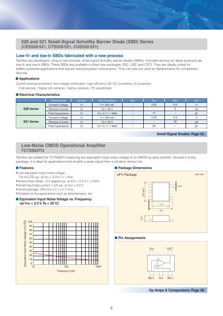
■ Electrical Characteristics<br />
Game consoles ●<br />
PC peripherals<br />
520 Series<br />
521 Series<br />
Characteristic<br />
Forward Voltage<br />
Reverse Current<br />
Total Capacitance<br />
Forward Voltage<br />
Reverse Current<br />
Total Capacitance<br />
Symbol<br />
VF<br />
IR<br />
CT<br />
VF<br />
IR<br />
CT<br />
Test Conditions<br />
IF = 200 mA<br />
VR = 30 V<br />
VR = 0, f = 1 MHz<br />
IF = 200 mA<br />
VR = 30 V<br />
VR = 0, f = 1 MHz<br />
Min<br />
–<br />
–<br />
–<br />
–<br />
–<br />
–<br />
Typ.<br />
0.52<br />
–<br />
17<br />
0.45<br />
–<br />
26<br />
Max<br />
0.6<br />
5<br />
–<br />
0.5<br />
30<br />
–<br />
Unit<br />
V<br />
μA<br />
pF<br />
V<br />
μA<br />
pF<br />
<strong>Small</strong>-<strong>Signal</strong> Diodes: Page 42-<br />
Low-Noise CMOS Operational Amplifier<br />
TC75S63TU<br />
Toshiba has added the TC75S63TU featuring low equivalent input noise voltage to its CMOS op amp portfolio. Housed in a tiny<br />
package, it is ideal for applications that amplify a weak signal from a vibration sensor, etc.<br />
■ Features<br />
● Low equivalent input noise voltage:<br />
7.8 nV/ Hz typ. at VDD = 3.3 V, f = 1 kHz<br />
● <strong>Small</strong> phase delay: –2.5 degree typ. at VDD = 3.3 V, f = 2 kHz<br />
● <strong>Small</strong> input bias current: 1 pA typ. at VDD = 3.3 V<br />
● <strong>Small</strong> package: UFV (2.0 x 2.1 x 0.7 mm)<br />
● Suitable for the applications such as shocksensors, etc.<br />
■ Package Dimensions<br />
UFV Package<br />
0.3<br />
Unit: mm<br />
■ Equivalent Input Noise Voltage vs. Frequency<br />
(at VDD = 3.3 V, Ta = 25°C)<br />
1.7<br />
2.1<br />
Equivalent Input Noise Voltage (nV/ Hz)<br />
100<br />
90<br />
80<br />
70<br />
60<br />
50<br />
40<br />
30<br />
20<br />
10<br />
0<br />
10 100<br />
Frequency (Hz)<br />
1000<br />
■ Pin Assignments<br />
VDD<br />
+<br />
–<br />
OUT<br />
IN(+) VSS IN(–)<br />
Op Amps & Comparators: Page 38-<br />
5