V386 rev 2-0.fm - SemiconductorStore.com
V386 rev 2-0.fm - SemiconductorStore.com
V386 rev 2-0.fm - SemiconductorStore.com

Create successful ePaper yourself
Turn your PDF publications into a flip-book with our unique Google optimized e-Paper software.
<strong>V386</strong><br />
8-BIT LVDS RECEIVER FOR VIDEO<br />
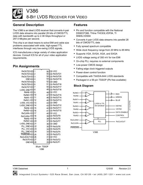
General Description<br />
The <strong>V386</strong> is an ideal LVDS receiver that converts 4-pair<br />
LVDS data streams into parallel 28 bits of CMOS/TTL<br />
data with bandwidth up to 2.38 Gbps throughput or<br />
297.5 Mbytes per second.<br />
This chip is an ideal means to solve EMI and cable size<br />
problems associated with wide, high-speed TTL<br />
interfaces through very low-swing LVDS signals.<br />
ICS manufactures a large variety of video application<br />
devices. Consult ICS for all of your video application<br />
requirements.<br />
Pin Assignments<br />
1<br />
2<br />
3<br />
56<br />
55<br />
54<br />
4<br />
53<br />
5<br />
52<br />
6<br />
51<br />
7<br />
50<br />
8<br />
49<br />
9<br />
48<br />
10 47<br />
11 46<br />
12 45<br />
13 44<br />
14 43<br />
15 42<br />
16 41<br />
17 40<br />
18 39<br />
19 38<br />
20 37<br />
21 36<br />
22 35<br />
23 34<br />
24 33<br />
25 32<br />
26 31<br />
27 30<br />
28 29<br />
VCC<br />
RxOUT21<br />
RxOUT20<br />
RxOUT19<br />
GND<br />
RxOUT18<br />
RxOUT17<br />
RxOUT16<br />
VCC<br />
RxOUT15<br />
RxOUT14<br />
RxOUT13<br />
GND<br />
RxOUT12<br />
RxOUT11<br />
RxOUT10<br />
VCC<br />
RxOUT9<br />
RxOUT8<br />
RxOUT7<br />
GND<br />
RxOUT6<br />
RxOUT5<br />
RxOUT4<br />
RxOUT3<br />
VCC<br />
RxOUT2<br />
RxOUT1<br />
Features<br />
• Pin and function <strong>com</strong>patible with the National<br />
DS90CF386, THine THC63LVDF84, TI<br />
SN65LVDS94<br />
• Converts 4-pair LVDS data streams into parallel 28<br />
bits of CMOS/TTL data<br />
• Fully spread spectrum <strong>com</strong>patible<br />
• Wide clock frequency range from 20 MHz to 85 MHz<br />
• Supports VGA, SVGA, XGA, and SXGA<br />
• LVDS voltage swing of 350 mV for low EMI<br />
• On-chip PLL requires no external <strong>com</strong>ponents<br />
• Low-power CMOS design<br />
• Falling edge clock triggered outputs<br />
• Power-down control function<br />
• Compatible with TIA/EIA-644 LVDS standards<br />
• Packaged in a 56-pin TSSOP (Pb free available)<br />
Block Diagram<br />
RxIN0+<br />
RxIN1+<br />
RxIN2+<br />
RxIN3+<br />
RxCLKIN-<br />
RxIN3-<br />
RxCLKIN+<br />
RxOUT22<br />
RxOUT23<br />
RxOUT24<br />
GND<br />
RxOUT25<br />
RxOUT26<br />
RxOUT27<br />
LVDS_GND<br />
RxIN0-<br />
RxIN0+<br />
RxIN1-<br />
RxIN1+<br />
LVDS_VCC<br />
LVDS_GND<br />
RxIN2-<br />
RxIN2+<br />
RxCLKIN-<br />
RxCLKIN+<br />
RxIN3-<br />
RxIN3+<br />
LVDS_GND<br />
PLL_GND<br />
PLL_VCC<br />
PLL_GND<br />
PWRDWN<br />
RxCLKOUT<br />
RxOUT0<br />
GND<br />
RxIN0-<br />
RxIN1-<br />
RxIN2-<br />
PWRDWN<br />
LVDS to TTL<br />
De-serializer<br />
<strong>V386</strong><br />
PLL<br />
8<br />
8<br />
8<br />
RED<br />
GREEN<br />
BLUE<br />
HSYNC<br />
VSYNC<br />
DATA ENABLE<br />
CONTROL<br />
RxCLKOUT<br />
RxOUT0..27<br />
56-pin TSSOP<br />
<strong>V386</strong><br />
<strong>V386</strong> Datasheet 1 12/5/05 Revision 2.0<br />
Integrated Circuit Systems • 525 Race Street, San Jose, CA 95126 • tel (408) 297-1201 • www.icst.<strong>com</strong>
<strong>V386</strong><br />
8-BIT LVDS RECEIVER FOR VIDEO<br />
Pin Descriptions<br />
Pin Pin name Type Description<br />
1 RxOUT22 OUT Data outputs on pins (RxOUT0..27)<br />
2 RxOUT23 OUT Data outputs on pins (RxOUT0..27)<br />
3 RxOUT24 OUT Data outputs on pins (RxOUT0..27)<br />
4 GND Ground Digital ground<br />
5 RxOUT25 OUT Data outputs on pins (RxOUT0..27)<br />
6 RxOUT26 OUT Data outputs on pins (RxOUT0..27)<br />
7 RxOUT27 OUT Data outputs on pins (RxOUT0..27)<br />
8 LVDS_GND Ground Analog ground<br />
9 RxIN0- LVDS IN LVDS input (-)<br />
10 RxIN0+ LVDS IN LVDS input (+)<br />
11 RxIN1- LVDS IN LVDS input (-)<br />
12 RxIN1+ LVDS IN LVDS input (+)<br />
13 LVDS_VCC Power Analog power<br />
14 LVDS_GND Ground Analog ground<br />
15 RxIN2- LVDS IN LVDS input (-)<br />
16 RxIN2+ LVDS IN LVDS input (+)<br />
17 RxCLKIN- LVDS IN LVDS input (-)<br />
18 RxCLKIN+ LVDS IN LVDS input (+)<br />
19 RxIN3- LVDS IN LVDS input (-)<br />
20 RxIN3+ LVDS IN LVDS input (+)<br />
21 LVDS_GND Ground Analog ground<br />
22 PLL_GND Ground PLL ground<br />
23 PLL_VCC Power PLL power<br />
24 PLL_GND Ground PLL ground<br />
25 PWRDWN IN Power-down control input.<br />
H: Nomal<br />
L: Power down, all ouputs are pulled low.<br />
26 RxCLKOUT OUT Clock output<br />
27 RxOUT0 OUT Data outputs on pins (RxOUT0..27)<br />
28 GND Ground Digital ground<br />
29 RxOUT1 OUT Data outputs on pins (RxOUT0..27)<br />
30 RxOUT2 OUT Data outputs on pins (RxOUT0..27)<br />
31 VCC Power Digital power<br />
32 RxOUT3 OUT Data outputs on pins (RxOUT0..27)<br />
33 RxOUT4 OUT Data outputs on pins (RxOUT0..27)<br />
<strong>V386</strong> Datasheet 2 12/5/05 Revision 2.0<br />
Integrated Circuit Systems • 525 Race Street, San Jose, CA 95126 • tel (408) 297-1201 • www.icst.<strong>com</strong>
<strong>V386</strong><br />
8-BIT LVDS RECEIVER FOR VIDEO<br />
Pin Pin name Type Description<br />
34 RxOUT5 OUT Data outputs on pins (RxOUT0..27)<br />
35 RxOUT6 OUT Data outputs on pins (RxOUT0..27)<br />
36 GND Ground Digital ground<br />
37 RxOUT7 OUT Data outputs on pins (RxOUT0..27)<br />
38 RxOUT8 OUT Data outputs on pins (RxOUT0..27)<br />
39 RxOUT9 OUT Data outputs on pins (RxOUT0..27)<br />
40 VCC Power Digital power<br />
41 RxOUT10 OUT Data outputs on pins (RxOUT0..27)<br />
42 RxOUT11 OUT Data outputs on pins (RxOUT0..27)<br />
43 RxOUT12 OUT Data outputs on pins (RxOUT0..27)<br />
44 GND Ground Digital ground<br />
45 RxOUT13 OUT Data outputs on pins (RxOUT0..27)<br />
46 RxOUT14 OUT Data outputs on pins (RxOUT0..27)<br />
47 RxOUT15 OUT Data outputs on pins (RxOUT0..27)<br />
48 VCC Power Digital power<br />
49 RxOUT16 OUT Data outputs on pins (RxOUT0..27)<br />
50 RxOUT17 OUT Data outputs on pins (RxOUT0..27)<br />
51 RxOUT18 OUT Data outputs on pins (RxOUT0..27)<br />
52 GND Ground Digital ground<br />
53 RxOUT19 OUT Data outputs on pins (RxOUT0..27)<br />
54 RxOUT20 OUT Data outputs on pins (RxOUT0..27)<br />
55 RxOUT21 OUT Data outputs on pins (RxOUT0..27)<br />
56 VCC Power Digital power<br />
.<br />
<strong>V386</strong> Datasheet 3 12/5/05 Revision 2.0<br />
Integrated Circuit Systems • 525 Race Street, San Jose, CA 95126 • tel (408) 297-1201 • www.icst.<strong>com</strong>
<strong>V386</strong><br />
8-BIT LVDS RECEIVER FOR VIDEO<br />
Absolute Maximum Ratings<br />
Stresses above the ratings listed below can cause permanent damage to the <strong>V386</strong>. These ratings, which are<br />
standard values for ICS <strong>com</strong>mercially rated parts, are stress ratings only. Functional operation of the device at<br />
these or any other conditions above those indicated in the operational sections of the specifications is not implied.<br />
Exposure to absolute maximum rating conditions for extended periods can affect product reliability. Electrical<br />
parameters are guaranteed only over the re<strong>com</strong>mended operating temperature range.<br />
Item<br />
Supply Voltage, VCC<br />
-0.3 V to +4 V<br />
CMOS/TTL Output Voltage -0.3 V to (VCC+0.3 V)<br />
LVDS Receiver Input Voltage -0.3 V to (VCC+0.3 V)<br />
Ambient Operating Temperature<br />
0 to +70°C<br />
Storage Temperature<br />
-65 to +150°C<br />
Junction Temperature 150°C<br />
Soldering Temperature (10 seconds max.) 260°C<br />
Maximum Package Power<br />
1.61 W (<strong>V386</strong>)<br />
Package Derating<br />
12.4 mW/°C above +25°C<br />
15 mW/°C above +25°C<br />
Rating<br />
Re<strong>com</strong>mended Operation Conditions<br />
Parameter Min. Typ. Max. Units<br />
Ambient Operating Temperature (Ta) 0 25 70 °C<br />
3.3 V Supply Voltage (VCC) 3 3.3 3.6 V<br />
Receiver Input Range (V IN ) 0 2.4 V<br />
Supply Noise Voltage (V N ) 100 mVpp<br />
Electrical Characteristics<br />
VDD=3.3 V ±10%, Ambient temperature 0 to 70°C<br />
Parameter Symbol Conditions Min. Typ. Max. Units<br />
CMOS/TTL DC Specifications<br />
Input High Voltage V IH 2.0 VCC V<br />
Input Low Voltage V IL GND 0.8 V<br />
Output High Voltage V OH I OH = -0.4 mA 2.7 3.3 VCC V<br />
Output Low Voltage V OL I OL = 2 mA 0.06 0.3 V<br />
Input Clamp Voltage V CL I CL = -18mA -0.79 -1.5 V<br />
Input Current I IN VCC ±15 µA<br />
<strong>V386</strong> Datasheet 4 12/5/05 Revision 2.0<br />
Integrated Circuit Systems • 525 Race Street, San Jose, CA 95126 • tel (408) 297-1201 • www.icst.<strong>com</strong>
<strong>V386</strong><br />
8-BIT LVDS RECEIVER FOR VIDEO<br />
Parameter Symbol Conditions Min. Typ. Max. Units<br />
0V ±10<br />
Output Short Circuit Current I OS V OUT = 0V -60 mA<br />
LVDS Receiver DC Specifications<br />
Differential Input High Threshold V TH V CM = +1.2 V +100 mV<br />
Differential Input Low Threshold V TL -100 mV<br />
Input Current I IN V IN = +2.4 V, VCC = 3.6 V ±10 µA<br />
V IN = 0V, VCC = 3.6 V ±15 µA<br />
Receiver Supply Current<br />
Receiver Supply Current (worst case) I CCRW C L = 8 pF, f = 65 MHz, worst<br />
220 mA<br />
case pattern<br />
C L = 8 pF, f = 85 MHz, worst<br />
case pattern<br />
240 mA<br />
Receiver Supply Current (16<br />
Grayscale)<br />
Receiver Supply Current (Power<br />
Down)<br />
Receiver Switching Characteristics<br />
I CCRG C L = 8 pF, f = 65 MHz, 16<br />
Grayscale pattern<br />
C L = 8 pF, f = 85 MHz, 16<br />
Grayscale pattern<br />
I CCRZ<br />
Power_Down = Low,<br />
Receiver outputs stay low<br />
during Power-down mode<br />
125 mA<br />
140 mA<br />
140 400 µA<br />
CMOS/TTL Low-to-High Transition CLHT 20% to 80% VCC, C L = 8 pF 2 3.5 ns<br />
Time<br />
CMOS/TTL High-to-Low Transition CHLT 80% to 20% VCC, C L = 8 pF 1.8 3.5 ns<br />
Time<br />
CLKOUT period RCOP 11.76 T 50 ns<br />
CLKOUT High Time RCOH f = 85 MHz 4.5 5 7 ns<br />
CLKOUT Low Time RCOL f = 85 MHz 4 5 6.5 ns<br />
Data Setup to CLKOUT RSRC f = 85 MHz 2.0 ns<br />
Data Hold to CLKOUT RHRC f = 85 MHz 3.5 ns<br />
RCK+/- to CLKOUT Delay RCCD 25°C / 3.3 V 8 14 20 ns<br />
Receiver PLL Setup Time RPLLS 10 ms<br />
Receiver Power Down Delay RPDD 1 µs<br />
Receiver Input Strobe Position for RSPos0 f = 85 MHz, T = 11.76 ns 0.49 0.84 1.19 ns<br />
Bit0<br />
Receiver Input Strobe Position for RSPos1 f = 85 MHz, T = 11.76 ns 2.17 2.52 2.87 ns<br />
Bit1<br />
Receiver Input Strobe Position for RSPos2 f = 85 MHz, T = 11.76 ns 3.85 4.2 4.55 ns<br />
Bit2<br />
Receiver Input Strobe Position for RSPos3 f = 85 MHz, T = 11.76 ns 5.53 5.88 6.23 ns<br />
Bit3<br />
Receiver Input Strobe Position for<br />
Bit4<br />
RSPos4 f = 85 MHz, T = 11.76 ns 7.21 7.56 7.91 ns<br />
<strong>V386</strong> Datasheet 5 12/5/05 Revision 2.0<br />
Integrated Circuit Systems • 525 Race Street, San Jose, CA 95126 • tel (408) 297-1201 • www.icst.<strong>com</strong>
<strong>V386</strong><br />
8-BIT LVDS RECEIVER FOR VIDEO<br />
Parameter Symbol Conditions Min. Typ. Max. Units<br />
Receiver Input Strobe Position for RSPos5 f = 85 MHz, T = 11.76 ns 8.89 9.24 9.59 ns<br />
Bit5<br />
Receiver Input Strobe Position for RSPos6 f = 85 MHz, T = 11.76 ns 10.57 10.92 11.27 ns<br />
Bit6<br />
RxIn Skew Margin (see note and Rskm f = 85 MHz, T = 11.76 ns 300 ps<br />
Figure 8)<br />
f = 65 MHz, T = 15.38 ns 500 ps<br />
Note: The skew margins mean the maximum timing tolerance between the clock and data channel when the<br />
receiver still works well. This margin takes into acount the receiver input setup and hold time, and internal clock<br />
jitter (i.e., internal data sampling window - RSPos). Thyis margin allows for LVDS transmitter pulse position,<br />
interconnect skew, inter-symbol interference and intrinsic channel mismatch which will cause the skew between<br />
clock (RC+ and RCK-) and data (RX[n]+ and RX[n]- ; n =0, 1, 2, 3) channels.<br />
Thermal Characteristics<br />
Parameter Symbol Conditions Min. Typ. Max. Units<br />
Thermal Resistance Junction to Ambient θ JA Still air 84 °C/W<br />
θ JA 1 m/s air flow 76 °C/W<br />
θ JA 3 m/s air flow 67 °C/W<br />
Thermal Resistance Junction to Case θ JC 50 °C/W<br />
<strong>V386</strong> Datasheet 6 12/5/05 Revision 2.0<br />
Integrated Circuit Systems • 525 Race Street, San Jose, CA 95126 • tel (408) 297-1201 • www.icst.<strong>com</strong>
<strong>V386</strong><br />
8-BIT LVDS RECEIVER FOR VIDEO<br />
Timing Diagrams<br />
CLKIN/CLKOUT<br />
ODD Data In/Data Out<br />
EVEN Data In/Data Out<br />
T<br />
Figure 1a. “Worst Case” Test Pattern<br />
CLKOUT<br />
D0, 8, 16<br />
D1, 9, 17<br />
D2, 10, 18<br />
D3, 11, 19<br />
D4-7, 12-15, 20-23<br />
D24-27<br />
Figure 1b. 16-Grayscale Test-Pattern Waveforms<br />
CMOS/TTL Output<br />
8pF<br />
80% 80%<br />
20% 20%<br />
CLHT<br />
CHLT<br />
<strong>V386</strong> CMO/TTL Output Load and Transition Times<br />
Figure 2. <strong>V386</strong> CMOS/TTL Output Load and Transition Time<br />
<strong>V386</strong> Datasheet 7 12/5/05 Revision 2.0<br />
Integrated Circuit Systems • 525 Race Street, San Jose, CA 95126 • tel (408) 297-1201 • www.icst.<strong>com</strong>
<strong>V386</strong><br />
8-BIT LVDS RECEIVER FOR VIDEO<br />
RCOP<br />
CLKOUT<br />
0.8 V<br />
2.0 V<br />
RCOH<br />
RSRC<br />
2.0 V<br />
0.8 V<br />
RCOL<br />
RHRC<br />
2.0 V<br />
D0 – D27 Out<br />
2.0 V<br />
SETUP<br />
2.0 V<br />
HOLD<br />
Figure 3. <strong>V386</strong> SETUP/HOLD and High/Low Times<br />
RCK<br />
Vdiff=0V<br />
RCCD<br />
CLKOUT<br />
1.5V<br />
Figure 4. <strong>V386</strong> Clock In to Clock Out Delay<br />
PWRDWN<br />
2.0 V<br />
3.0 V<br />
3.6 V<br />
VCC<br />
RPLLS<br />
RCK<br />
CLKOUT<br />
Figure 5. <strong>V386</strong> Phase Lock Loop Set Time<br />
1.5 V<br />
PWRDWN<br />
RCK IN<br />
RPDD<br />
Low<br />
Figure 6. <strong>V386</strong> Power Down Delay<br />
<strong>V386</strong> Datasheet 8 12/5/05 Revision 2.0<br />
Integrated Circuit Systems • 525 Race Street, San Jose, CA 95126 • tel (408) 297-1201 • www.icst.<strong>com</strong>
<strong>V386</strong><br />
8-BIT LVDS RECEIVER FOR VIDEO<br />
TCLK<br />
Clock<br />
P<strong>rev</strong>ious Cycle<br />
Next Cycle<br />
Data<br />
Rspos0 Min<br />
Rspos0 Max<br />
Rspos1 Min<br />
Rspos1 Max<br />
Rspos2 Min<br />
Rspos2 Max<br />
Rspos3 Min<br />
Rspos3 Max<br />
Rspos4 Min<br />
Rspos4 Max<br />
Rspos5 Min<br />
Rspos5 Max<br />
Rspos6 Min<br />
Rspos6 Max<br />
Figure 7. <strong>V386</strong> LVDS Input Strobe Position<br />
RCK+/RCK-<br />
RX[n]+/RX[n]-<br />
N = 0, 1, 2, 3<br />
Skew Margin<br />
Figure 8. Receiver Input Skew Margin<br />
<strong>V386</strong> Datasheet 9 12/5/05 Revision 2.0<br />
Integrated Circuit Systems • 525 Race Street, San Jose, CA 95126 • tel (408) 297-1201 • www.icst.<strong>com</strong>
<strong>V386</strong><br />
8-BIT LVDS RECEIVER FOR VIDEO<br />
Package Outline and Package Dimensions (56-pin TSSOP)<br />
Package dimensions are kept current with JEDEC Publication No. 95<br />
56<br />
Millimeters<br />
Inches*<br />
Symbol Min Max Min Max<br />
INDEX<br />
AREA<br />
1 2<br />
D<br />
E1<br />
E<br />
A — 1.20 — 0.047<br />
A1 0.05 0.15 0.002 0.006<br />
A2 0.80 1.05 0.032 0.041<br />
b 0.17 0.27 0.007 0.011<br />
C 0.09 0.20 0.0035 0.008<br />
D 13.90 14.10 0.547 0.555<br />
E 8.10 BASIC 0.319 BASIC<br />
E1 6.00 6.20 0.236 0.244<br />
e 0.50 BASIC 0.020 BASIC<br />
L 0.45 0.75 0.018 0.030<br />
a 0° 8° 0° 8°<br />
aaa — 0.10 — 0.004<br />
A<br />
2<br />
A<br />
* For reference only. Controlling dimensions in mm.<br />
A<br />
1<br />
- C -<br />
c<br />
e<br />
b<br />
SEATING<br />
PLANE<br />
aaa C<br />
α<br />
L<br />
Ordering Information<br />
Part / Order Number Marking Shipping Packaging Package Temperature<br />
<strong>V386</strong>G <strong>V386</strong>G Tubes 56-pin TSSOP 0 to +70°C<br />
<strong>V386</strong>GT <strong>V386</strong>G Tape and Reel 56-pin TSSOP 0 to +70°C<br />
<strong>V386</strong>GLF <strong>V386</strong>GLF Tubes 56-pin TSSOP 0 to +70°C<br />
<strong>V386</strong>GLFT <strong>V386</strong>GLF Tape and Reel 56-pin TSSOP 0 to +70°C<br />
Parts that are ordered with a "LF" suffix to the part number are the Pb-Free configuration and are RoHS <strong>com</strong>pliant.<br />
While the information presented herein has been checked for both accuracy and reliability, Integrated Circuit<br />
Systems (ICS) assumes no responsibility for either its use or for the infringement of any patents or other rights of<br />
third parties, which would result from its use. No other circuits, patents, or licenses are implied. This product is<br />
intended for use in normal <strong>com</strong>mercial applications. Any other applications such as those requiring extended<br />
temperature range, high reliability, or other extraordinary environmental requirements are not re<strong>com</strong>mended<br />
without additional processing by ICS. ICS reserves the right to change any circuitry or specifications without notice.<br />
ICS does not authorize or warrant any ICS product for use in life support devices or critical medical instruments.<br />
<strong>V386</strong> Datasheet 10 12/5/05 Revision 2.0<br />
Integrated Circuit Systems • 525 Race Street, San Jose, CA 95126 • tel (408) 297-1201 • www.icst.<strong>com</strong>