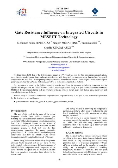
Gate Resistance Influence on Integrated Circuits in MESFET ...
Gate Resistance Influence on Integrated Circuits in MESFET ...
Gate Resistance Influence on Integrated Circuits in MESFET ...

Create successful ePaper yourself
Turn your PDF publications into a flip-book with our unique Google optimized e-Paper software.
SETIT 2007<br />
4 th Internati<strong>on</strong>al C<strong>on</strong>ference: Sciences of Electr<strong>on</strong>ic,<br />
Technologies of Informati<strong>on</strong> and Telecommunicati<strong>on</strong>s<br />
March 25-29, 2007 – TUNISIA<br />
<str<strong>on</strong>g>Gate</str<strong>on</strong>g> <str<strong>on</strong>g>Resistance</str<strong>on</strong>g> <str<strong>on</strong>g>Influence</str<strong>on</strong>g> <strong>on</strong> <strong>Integrated</strong> <strong>Circuits</strong> <strong>in</strong><br />
<strong>MESFET</strong> Technology<br />
Mohamed Salah BENBOUZA * , Nadjim MERABTINE ** , Yasm<strong>in</strong>a Saidi *** ,<br />
Cherifa KENZAI-AZIZI ***<br />
* Département d’électrotechnique Faculté des Sciences Université de Batna Algeria.<br />
** Laboratoire Electromagnétisme et Télécommunicati<strong>on</strong>s Université de C<strong>on</strong>stant<strong>in</strong>e Algeria.<br />
*** Laboratoire Physique des Couches M<strong>in</strong>ces et Interfaces Université de C<strong>on</strong>stant<strong>in</strong>e Algeria.<br />
benb5506@yahoo.fr<br />
merabt<strong>in</strong>enadjim@yahoo.fr<br />
aziziche@yahoo.fr<br />
Abstract S<strong>in</strong>ce 1961 date of the first <strong>in</strong>tegrated circuit to 1971 which has seen the first microprocessor applicati<strong>on</strong>,<br />
the micro-electr<strong>on</strong>ics passed from a discrete transistor to MSI <strong>in</strong>tegrated circuits with many thousands of <strong>in</strong>tegrated<br />
comp<strong>on</strong>ents and now to VLSI <strong>in</strong>tegrat<strong>in</strong>g many hundreds of thousands of devices. Technological recent technological<br />
progress permitted the GaAs and its ternary derivative to be the sec<strong>on</strong>d generati<strong>on</strong> material.<br />
So, we present a study <strong>on</strong> the Gallium arsenide material specify<strong>in</strong>g its transport and electric properties, and its<br />
specific advantages over the silic<strong>on</strong> material. A semi <strong>in</strong>sulat<strong>in</strong>g substrate study of a gate Schottky diode for the GaAs<br />
<strong>MESFET</strong> devices manufactur<strong>in</strong>g such as structures with and without buffer layer, with buried gate, mushroom and<br />
several f<strong>in</strong>gers are carried over.<br />
We will study the <strong>in</strong>fluence of the <strong>in</strong>put impedance and output resistance to the gate as well as the noise generated<br />
by the structures to several f<strong>in</strong>gers.<br />
Key words: GaAs <strong>MESFET</strong>, gate <strong>in</strong> T and PI, gate resistance, noise.<br />
INTRODUCTION<br />
The aim of this work is the study of the logical<br />
<strong>in</strong>tegrated circuits based gallium arsenide gate<br />
Schottky field-effect transistors called GaAs <strong>MESFET</strong>.<br />
As a matter of fact, the <strong>in</strong>tegrated circuits development<br />
has a very important impact <strong>on</strong> the whole of<br />
electr<strong>on</strong>ics effectively, s<strong>in</strong>ce 1961 dates from the first<br />
<strong>in</strong>tegrated circuit, to 1971 that saw the first<br />
microprocessor appariti<strong>on</strong>, the micro electr<strong>on</strong>ics<br />
passed from to LSI circuits with thousand of <strong>in</strong>tegrated<br />
comp<strong>on</strong>ents and now to circuits VLSI circuits<br />
<strong>in</strong>tegrat<strong>in</strong>g several hundreds of thousands of devices.<br />
In this study, we are first <strong>in</strong>terested by the gallium<br />
arsenide GaAs material that is the bases of this<br />
technological evoluti<strong>on</strong>, then to different structures of<br />
<strong>MESFET</strong> GaAs comp<strong>on</strong>ent which composes a choice<br />
device for the c<strong>on</strong>cepti<strong>on</strong> and the realizati<strong>on</strong> of ultra<br />
fast logic circuits at propagati<strong>on</strong> time <strong>in</strong>ferior to the<br />
nanosec<strong>on</strong>d.<br />
Our survey c<strong>on</strong>sists <strong>in</strong> improv<strong>in</strong>g the comp<strong>on</strong>ent’s<br />
performance: to have a low noise by reduc<strong>in</strong>g the gate<br />
length, m<strong>in</strong>imiz<strong>in</strong>g the parasitic’ sources and reduc<strong>in</strong>g<br />
the gate resistances.<br />
We will study, at a given frequency, the noise<br />
variati<strong>on</strong>s respectively accord<strong>in</strong>g to the channel length<br />
and width. We will also study particularly the<br />
capacitive effect of the resistance Rg at microwave and<br />
millimetre –length wave frequencies<br />
1. GaAs material<br />
The choice of GaAs as material permitt<strong>in</strong>g to obta<strong>in</strong><br />
very high performances for the <strong>in</strong>tegrated circuits is not<br />
<strong>on</strong>ly related to very <strong>in</strong>terest<strong>in</strong>g semi- c<strong>on</strong>duct<strong>in</strong>g<br />
properties but to a propitious compromise between<br />
different criteri<strong>on</strong> such as the metallurgic properties,<br />
ability to technological realisati<strong>on</strong> ,work<strong>in</strong>g<br />
temperature, tolerance to radiati<strong>on</strong>s. The last year<br />
technological progress permitted GaAs and its ternary<br />
derivatives to be the sec<strong>on</strong>d generati<strong>on</strong> material.<br />
-1-
SETIT2007<br />
1.1. Transport properties<br />
The N type gallium arsenide presents excellent<br />
transport properties [1]. For weak values of the dop<strong>in</strong>g<br />
of material dop<strong>in</strong>g, mobility at weak field can reach<br />
values of 8000-9000 cm2/Vs at the ambient temperature<br />
(10000 to 80000 cm2/Vs with 77 ° K). At the usual dop<strong>in</strong>g<br />
(10 17 .Cm -3 ), the electr<strong>on</strong>s mobility is six times higher <strong>in</strong><br />
GaAs than <strong>in</strong> the Si and their transport speed is twice<br />
(higher) faster. The speed saturati<strong>on</strong> at high electric<br />
field is reached for an electric field less higher than the<br />
Si. As a result ,the transit time of GaAs <strong>MESFET</strong><br />
with gate length between 0.5 and 0.1 µm is of the<br />
order of 10 to 20 picosec<strong>on</strong>ds corresp<strong>on</strong>d<strong>in</strong>g to cut-off<br />
frequencies of ga<strong>in</strong> the product <strong>in</strong>current - pass bandbetween<br />
20 to 30 GHz. For a similar c<strong>on</strong>cepti<strong>on</strong>, we<br />
po<strong>in</strong>t out merit factor for to six times superior to those<br />
obta<strong>in</strong>ed <strong>on</strong> silic<strong>on</strong> JFET devices.<br />
.<br />
1.2. Electric Properties<br />
The electric properties of GaAs with 300 °K<br />
<strong>in</strong>terven<strong>in</strong>g <strong>in</strong> the discrete or <strong>in</strong>tegrated circuits<br />
manufacture are gathered <strong>in</strong> table 1.<br />
PROPERTIES GaAs Si<br />
forbidden band 1.43eV 1.12eV<br />
Energy<br />
forbidden band Type Direct Indirect<br />
State density <strong>in</strong> the 5.10 17 cm -3 5.10 19 cm -3<br />
c<strong>on</strong>ducti<strong>on</strong> band<br />
Charge at MIS 10 13 cm -3 10 10 cm -3<br />
<strong>in</strong>terface<br />
Life durati<strong>on</strong> of the 10 8 s 10 4 s<br />
m<strong>in</strong>ority carriers<br />
critical field at high 3.10 2 Vcm -1 1.10 2 Vcm -1<br />
field mode<br />
Break-down field 4.10 5 Vcm -1 3.10 5 Vcm -1<br />
Schottky barrier 0.7-0.8V 0.4-0.6V<br />
height<br />
Electr<strong>on</strong>ic mobility at 4900cm 2 V -1 s -1 800cm 2 V -1 s -1<br />
Nd=10 17 Cm -3<br />
holes mobility 250cm 2 V -1 s -1 350cm 2 V -1 s -1<br />
electr<strong>on</strong>s mobility 1.10 7 cms -1 1.10 9 cms -1<br />
speed<br />
Maximale resistivity 10 9 cm 10 9 cm<br />
Table 1: Ma<strong>in</strong> properties of GaAs and Si at 300°K<br />
1.3. Semi-<strong>in</strong>sulat<strong>in</strong>g substrate<br />
The semi <strong>in</strong>sulat<strong>in</strong>g GaAs material availability [2]<br />
(resistivity <strong>in</strong>cluded between l0 7 and l0 9 cm with<br />
T=300°K°) is a substantial advantage from technological<br />
and electrical performance po<strong>in</strong>t of view. The <strong>in</strong>ter device<br />
<strong>in</strong>sulati<strong>on</strong> is ensured without circuits performances<br />
damage: thus the parasitic capacities l<strong>in</strong>ked to the mass<br />
plan rema<strong>in</strong> <strong>in</strong>ferior to the coplanar parasitic capacities of<br />
dra<strong>in</strong>- source c<strong>on</strong>tacts <strong>in</strong>terc<strong>on</strong>necti<strong>on</strong>s l<strong>in</strong>es.<br />
The obta<strong>in</strong><strong>in</strong>g method of semi-<strong>in</strong>sulat<strong>in</strong>g GaAs<br />
substrates c<strong>on</strong>sists <strong>in</strong> compensat<strong>in</strong>g the residual levels<br />
obta<strong>in</strong>ed materials us<strong>in</strong>g the of Bridgman method by a<br />
specifically deep impurity; the chrome be<strong>in</strong>g mostly<br />
used. The use of i<strong>on</strong>ic implantati<strong>on</strong> of the chrome<br />
doped GaAs obta<strong>in</strong>ed by Bridgman growth revealed<br />
anomalies appear<strong>in</strong>g dur<strong>in</strong>g the anneal<strong>in</strong>g after<br />
implantati<strong>on</strong>.<br />
The phenomen<strong>on</strong> tied to the Cr oxodiffusi<strong>on</strong> dur<strong>in</strong>g<br />
the thermal treatment is identical to the <strong>on</strong>e met <strong>on</strong><br />
epitaxied layers <strong>on</strong> Cr doped GaAs.<br />
2. GaAs <strong>MESFET</strong> transistors<br />
manufacture<br />
On GaAs, the base comp<strong>on</strong>ent is <strong>in</strong> fact the<br />
Schottky gate field-effect transistor called <strong>MESFET</strong><br />
(Metal Semic<strong>on</strong>ductor Field Effect- Transistor) which<br />
is a majority carriers device, its structure is<br />
particularly simple easily realizable <strong>in</strong> N type th<strong>in</strong><br />
layer. This <strong>MESFET</strong> active layer is a th<strong>in</strong> c<strong>on</strong>duct<strong>in</strong>g<br />
uniform layer with a thickness d (1000-2000) with<br />
can vary dop<strong>in</strong>g between 10 16 and 3.10 17 Cm -3<br />
accord<strong>in</strong>g to the structure, N doped by means of<br />
sulphur or t<strong>in</strong> some time . The active layer growth is<br />
realized by various technologies [3]:<br />
- Liquid phase epitaxy, the later does not allow a<br />
strict c<strong>on</strong>trol thickness d.<br />
- molecular jets epitaxy [4] that allows an<br />
excellent c<strong>on</strong>trol of active layer thickness(a few<br />
thousands of Angströms – layer ) and is particularly<br />
well adapted to the GaAs <strong>MESFET</strong> realizati<strong>on</strong> ,of<br />
normally blocked said Normally OFF.<br />
- I<strong>on</strong>ic implantati<strong>on</strong>, this semi isolat<strong>in</strong>g dop<strong>in</strong>g<br />
technique permits to realise layers with properties<br />
similar to those obta<strong>in</strong>ed by epitaxy and present<br />
certa<strong>in</strong> advantages for the reproducibility and<br />
structure homogeneity.<br />
- Vapor phase epitaxy by metallic device or<br />
chlorids [4] is the softest method and the most<br />
adapted to the <strong>in</strong>dustrial treatment; it actually<br />
rema<strong>in</strong>s the privileged toolt for the discrete devices.<br />
The N layer regi<strong>on</strong> (figure 1-a) form the active<br />
area. The source -dra<strong>in</strong> c<strong>on</strong>tact are composed by<br />
an “eutectique “obta<strong>in</strong>ed by an alloy (400-500°C)<br />
of thr gold germanium layer with GaAs.<br />
Metallizati<strong>on</strong> of nearly 0.5 µm thicknesses<br />
formed by a titanium gold compo doposit ensure the<br />
device <strong>in</strong>terc<strong>on</strong>necti<strong>on</strong>s with the elements.<br />
The <strong>MESFET</strong> ma<strong>in</strong> advantage is the particularly<br />
simple gate structure that always to reduce its<br />
geometry to extreme values comparatively to other<br />
transistors.<br />
It is sufficient to engrave <strong>on</strong> GaAs the metallic<br />
band that forms the grate. For the <strong>in</strong>tegrated circuits,<br />
the typical length is of 1µm but the actual tendency is<br />
to pass to the submicr<strong>on</strong>ics geometries. the gate length<br />
which determ<strong>in</strong>es at the time the <strong>in</strong>put capacity <strong>on</strong> the<br />
electr<strong>on</strong>s transit time <strong>in</strong> the channel c<strong>on</strong>diti<strong>on</strong>s the<br />
performances at average velocity of 10 7 cm.s -1 , leads<br />
to a 10 ps a transit time and a current ga<strong>in</strong> cut-off<br />
- 2 -
SETIT2007<br />
frequency of the order of 15 GHz. Tak<strong>in</strong>g the new<br />
possibilities <strong>in</strong> micro lithography <strong>in</strong>to c<strong>on</strong>siderati<strong>on</strong>,<br />
the microelectr<strong>on</strong>ics <strong>on</strong> GaAs is more advanced than<br />
silic<strong>on</strong> technology.<br />
2.1. Structure with and without buffer layer<br />
The first transistor as be<strong>in</strong>g realised by means of<br />
epitaxial layers directly deposited <strong>on</strong> semi -<strong>in</strong>sulat<strong>in</strong>g<br />
substrate (figure 1-a)<br />
2.2. Ploughed or buried gate GaAs <strong>MESFET</strong>”<br />
In GaAs and for a free face, there is potential<br />
barrier near the surface <strong>on</strong>e (figure 2). This latter is<br />
expressed by the space charge density existence,<br />
extend<strong>in</strong>g <strong>in</strong> the dra<strong>in</strong> gate and source gate -<br />
space.<br />
Source<br />
Dra<strong>in</strong><br />
Z<br />
L<br />
<str<strong>on</strong>g>Gate</str<strong>on</strong>g><br />
Source<br />
<str<strong>on</strong>g>Gate</str<strong>on</strong>g><br />
Dra<strong>in</strong><br />
Active layer<br />
N<br />
N<br />
Substrate<br />
Semi – <strong>in</strong>sulat<strong>in</strong>g substrate<br />
Figure 2 L<strong>on</strong>gitud<strong>in</strong>al secti<strong>on</strong> of the <strong>MESFET</strong> with<br />
buried gate.<br />
Source<br />
(a)<br />
L<br />
Z<br />
<str<strong>on</strong>g>Gate</str<strong>on</strong>g><br />
Active layer<br />
Buffer<br />
Semi – <strong>in</strong>sulat<strong>in</strong>g substrate<br />
Dra<strong>in</strong><br />
N<br />
It follows a noticeable <strong>in</strong>crease <strong>in</strong> access<br />
resistances. The latter limit the current which is then<br />
badly c<strong>on</strong>trolled by the gate (particularly for the<br />
weak gate polarizati<strong>on</strong> or lightly positive) . To<br />
improve the transistor command, we realise a buried<br />
gate. This structure is realised by groov<strong>in</strong>g us<strong>in</strong>g by<br />
a chemic attack or plasma engrav<strong>in</strong>g, a trench <strong>in</strong> the<br />
semic<strong>on</strong>ductor between the source and dra<strong>in</strong><br />
c<strong>on</strong>tacts. Then the gate metal is pulverized at the<br />
very bottom of this trench. By this method we<br />
reduce the access resistances to the <strong>in</strong>tr<strong>in</strong>sic regi<strong>on</strong> of<br />
the comp<strong>on</strong>ent (under the gate) due the lateral regi<strong>on</strong><br />
unc<strong>on</strong>trolled by the gate. This process presents,<br />
however, the disadvantage to <strong>in</strong>crease the<br />
technological operati<strong>on</strong>s complexity .we often prefers<br />
the locad i<strong>on</strong>ic implantati<strong>on</strong> technics that permit to<br />
over dope the <strong>in</strong>ter electrode regi<strong>on</strong>s and c<strong>on</strong>sequently<br />
to decrease the access resistances by selectively<br />
<strong>in</strong>creas<strong>in</strong>g the d<strong>on</strong>ors density Nd (N type<br />
semic<strong>on</strong>ductor N type) under the lateral regi<strong>on</strong>s.<br />
(b)<br />
Figure 1 Structure of the GaAs <strong>MESFET</strong>; (a)<br />
<strong>MESFET</strong> without buffer layer; (b) <strong>MESFET</strong><br />
with buffer layer<br />
Their performances have be<strong>in</strong>g affected by effects<br />
by hysteresis. Is effect <strong>in</strong> order to m<strong>in</strong>imize the<br />
activate substrate <strong>in</strong>terface layer, it has became<br />
classical to <strong>in</strong>sert an epitaxial layer called “buffer”<br />
weakly doped (10 12 to 10 11 cm -3 ) and which the average<br />
thickness is of 1the order 10 µm (figure 1 - b).<br />
In order to improve the device performances,<br />
several manufacture techniques has be<strong>in</strong>g proposed<br />
.We will present some of them [5].<br />
2.3. Buffer layer structure GaAs <strong>MESFET</strong><br />
To improve the GaAs <strong>MESFET</strong> commutati<strong>on</strong> and<br />
hyper frequency performances many gate<br />
c<strong>on</strong>figurati<strong>on</strong> are c<strong>on</strong>sidered figure (3-a) shows a<br />
structure with semi <strong>in</strong>sulat<strong>in</strong>g gate, manufactured by<br />
Ar bomb<strong>in</strong>g of the gate regi<strong>on</strong>. The device can<br />
reduce the capacity, reduce also gate the leakage<br />
current and <strong>in</strong>crease the tensi<strong>on</strong> of breakdown<br />
voltage. The figure (3-b) shows a similar structure<br />
with a gate <strong>in</strong> “buffer”. This layer is <strong>in</strong>serted between<br />
the gate metal and the active layer, the self-align<strong>in</strong>g<br />
technics has be<strong>in</strong>g used to realised comp<strong>on</strong>ents with<br />
submicr<strong>on</strong>ic gate length.<br />
- 3 -
SETIT2007<br />
Source <str<strong>on</strong>g>Gate</str<strong>on</strong>g> Dra<strong>in</strong><br />
<str<strong>on</strong>g>Gate</str<strong>on</strong>g><br />
Bombardment of Ar+<br />
Depleti<strong>on</strong> Z<strong>on</strong>e<br />
Source<br />
Source<br />
Semi- <strong>in</strong>sulat<strong>in</strong>g substrate<br />
(a)<br />
Dra<strong>in</strong><br />
Source<br />
<str<strong>on</strong>g>Gate</str<strong>on</strong>g><br />
Dra<strong>in</strong><br />
(b)<br />
Figure 4 T and PI GaAs <strong>MESFET</strong> structures; (a) T<br />
GaAs <strong>MESFET</strong>; (b) PI GaAs <strong>MESFET</strong><br />
Layer Tamp<strong>on</strong><br />
Depleti<strong>on</strong> Z<strong>on</strong>e<br />
Semi- <strong>in</strong>solat<strong>in</strong>g substrate<br />
(b)<br />
Figure 3 Structure GaAs <strong>MESFET</strong> with buffer layer;<br />
(a) <str<strong>on</strong>g>Gate</str<strong>on</strong>g> bombardment with Arg<strong>on</strong> I<strong>on</strong>s; (b): <str<strong>on</strong>g>Gate</str<strong>on</strong>g> buffer<br />
layer<br />
3. Equivalent circuit of the <strong>MESFET</strong><br />
The equivalent circuit of a comp<strong>on</strong>ent MMIC must<br />
sufficiently represent all the important physical<br />
characteristics of the device and exploit the<br />
relati<strong>on</strong>ship between the equivalent elements of the<br />
circuit and physique of the device which will be useful<br />
<strong>in</strong> the mathematical formulati<strong>on</strong>.<br />
Transistor <strong>MESFET</strong> and HEMT to study is<br />
represented <strong>on</strong> figure 5-a. the structure which<br />
determ<strong>in</strong>es the behaviour of microwave of a transistor<br />
<strong>MESFET</strong> is identified <strong>on</strong> the figure 5-b; some of<br />
parameters important are deferred <strong>in</strong> [6], [7].<br />
2.4. T and PI GaAs <strong>MESFET</strong> structures<br />
<str<strong>on</strong>g>Gate</str<strong>on</strong>g><br />
Dra<strong>in</strong><br />
Source<br />
Dra<strong>in</strong><br />
(a)<br />
(a)<br />
- 4 -
SETIT2007<br />
f<strong>in</strong>gers. The sk<strong>in</strong> effect will present the frequency<br />
resp<strong>on</strong>se <strong>in</strong> the metallizati<strong>on</strong> access resistance of the<br />
gate <strong>in</strong> AC regime [4]:<br />
r<br />
f<br />
( f ) = rga<br />
1<br />
(3)<br />
fse<br />
ae<br />
ga<br />
+<br />
(b)<br />
Figure 5 Parameters of <strong>MESFET</strong>; (a) geometrical<br />
parameters; (b) equivalent circuit <strong>in</strong> high frequency<br />
Where: N is the dop<strong>in</strong>g density <strong>in</strong> the N layer of the<br />
channel, W is the thickness of the layer N of the<br />
channel under the gate, Z G is the width of the gate, L G<br />
is the length of the metal gate, L SG is the separati<strong>on</strong><br />
gate - source, L GD is the separati<strong>on</strong> gate – dra<strong>in</strong>, W R the<br />
depressi<strong>on</strong> depth of the gate, Ws is the exhausti<strong>on</strong><br />
depth of the surface, d is the depth of exhausti<strong>on</strong>, h is<br />
the height of the gate, X is the extensi<strong>on</strong> of the gate<br />
charge space under the gate.<br />
4. <str<strong>on</strong>g>Influence</str<strong>on</strong>g> of gate resistance <strong>on</strong> the<br />
<strong>in</strong>put impedance<br />
<str<strong>on</strong>g>Resistance</str<strong>on</strong>g> associated to the gate metallizati<strong>on</strong><br />
deteriorates the microwaves and commutati<strong>on</strong><br />
performances. To carry out weak noise <strong>MESFET</strong>, it is<br />
important to decrease the gate resistance. This gate<br />
resistance Rg was identified a l<strong>on</strong>g time as a parasitic<br />
parameter which deteriorates the noise factor and<br />
limits the power ga<strong>in</strong> of the Schottky-barrier-gate<br />
<strong>MESFET</strong>S (SBG<strong>MESFET</strong>s). We add a metallizati<strong>on</strong><br />
resistance: Rga to Rg as shown <strong>on</strong> the figure 5-b .this<br />
gate metallizati<strong>on</strong> resistance c<strong>on</strong>tributes clearly to Rg<br />
[8]. It is given <strong>in</strong> a distributed way, and c<strong>on</strong>firms the<br />
effect of the resistance end to end of the gate f<strong>in</strong>ger:<br />
rga<br />
Wg<br />
Rga = (1)<br />
3Nk²<br />
To dist<strong>in</strong>guish this well-known resistance from the<br />
comp<strong>on</strong>ent <strong>MESFET</strong> which is the aim of this article,<br />
we presented this access resistance al<strong>on</strong>g the gate<br />
f<strong>in</strong>ger rga ,it is then the end to end normal<br />
metallizati<strong>on</strong> resistance given by:<br />
<br />
r<br />
ga<br />
= (2)<br />
A<br />
gx<br />
Where is the metal resistivity of gate , and Agx is<br />
the gate secti<strong>on</strong> . Wg is the gate and Nk is the number<br />
of parallel f<strong>in</strong>gers. Because the undercarriage length of<br />
door is narrowed with major submicr<strong>on</strong>ic dimensi<strong>on</strong>s it<br />
is usual to limit the <strong>in</strong>crease <strong>in</strong> the rga by us<strong>in</strong>g a<br />
formed cut T, and to <strong>in</strong>crease the number of parallel<br />
where the frequency characteristic for the<br />
beg<strong>in</strong>n<strong>in</strong>g of the significant sk<strong>in</strong> effect is:<br />
fse<br />
r<br />
ga<br />
= β<br />
(4)<br />
µo<br />
µo = 4.10-7 Vs/Am is the free space permeability,<br />
and a geometrical factor, roughly equal to 3,5 for a<br />
cross secti<strong>on</strong> of the cross-secti<strong>on</strong>. For a rga=150<br />
/mm, the fse is 420 GHz. Although can be reduced<br />
by the presence of a plane <strong>on</strong> the ground [5], the sk<strong>in</strong><br />
effect seems certa<strong>in</strong>ly to be negligible. We prove<br />
numerically that the sk<strong>in</strong> effect is <strong>in</strong>deed negligible,<br />
and that eqns. (3) - (4) are precise and adapted for<br />
SBG<strong>MESFET</strong>. Another resistive comp<strong>on</strong>ent <strong>on</strong> the<br />
<strong>in</strong>put side of the <strong>MESFET</strong> is the fill<strong>in</strong>g resistance Ri<br />
(or Rgs) for the gate - source capacity. This parameter<br />
is often hard to separate from Rg dur<strong>in</strong>g the extracti<strong>on</strong><br />
of the equivalent circuit [6]. However, Ri is between a<br />
sixth and a fifth of the channel resistance for a used<br />
zero-dra<strong>in</strong>-polarizati<strong>on</strong> [7].<br />
1 Lg Idmax Lg.vsat<br />
Ri Ro( )( ) =<br />
5 Wg Id 5µId<br />
= (5)<br />
Where Ro is the plate resistance and Idmax the<br />
current saturati<strong>on</strong> of the channel, vsat is the speed of<br />
saturati<strong>on</strong>, and µ the mobility. The factor 1/5 <strong>in</strong> eqn.<br />
(5) is the higher limit of quantity:<br />
(R11-R12)/ (I11-I12) 2<br />
Where Rij and Iij parameters determ<strong>in</strong>e the Y<br />
parameters, and are derived from the waves l<strong>in</strong>ear<br />
equati<strong>on</strong> of the <strong>MESFET</strong> <strong>in</strong>side [8]. It expla<strong>in</strong>s both<br />
the distributed nature of Ri, and the change of the<br />
electr<strong>on</strong> c<strong>on</strong>centrati<strong>on</strong> of the sheet al<strong>on</strong>g the channel.<br />
Both eqns. (1) and (5) foresee very small resistances,<br />
often much smaller than the values produced by<br />
methods of extracti<strong>on</strong> of equivalent circuit. It is an<br />
<strong>in</strong>dicati<strong>on</strong> of an additi<strong>on</strong>al comp<strong>on</strong>ent <strong>in</strong> the <strong>in</strong>put<br />
resistance, whose physics must be established <strong>in</strong> order<br />
to understand better the <strong>MESFET</strong> comp<strong>on</strong>ent, and to<br />
produce measurable models. To f<strong>in</strong>ish the study of<br />
effect of the c<strong>on</strong>duct<strong>in</strong>g semi metal <strong>in</strong>terface, we add a<br />
comp<strong>on</strong>ent to Rg resistance [10] which def<strong>in</strong>es the<br />
gate resistance f the normalized <strong>in</strong>terfacial resistance<br />
.This resistance is def<strong>in</strong>ed as a c<strong>on</strong>tact resistance with<br />
the substrate, rgi be<strong>in</strong>g the normal gate resistance of<br />
the normalized <strong>in</strong>terfacial resistance.<br />
Rgi<br />
r<br />
gi<br />
= (6)<br />
WgLg<br />
Simulati<strong>on</strong> AC of the <strong>in</strong>fluence of the gate<br />
resistance and gate length <strong>on</strong> the <strong>in</strong>put and output<br />
- 5 -
SETIT2007<br />
impedance of GaAs <strong>MESFET</strong> transistors are<br />
represented <strong>on</strong> figures 6, 7 and 8.<br />
Figure 6 <str<strong>on</strong>g>Gate</str<strong>on</strong>g> <strong>in</strong>fluence <strong>on</strong> Z <strong>in</strong><br />
Figure 7 <str<strong>on</strong>g>Gate</str<strong>on</strong>g> <strong>in</strong>fluence <strong>on</strong> C <strong>in</strong><br />
Figure 8 <str<strong>on</strong>g>Gate</str<strong>on</strong>g> <strong>in</strong>fluence <strong>on</strong> R out<br />
5. <str<strong>on</strong>g>Influence</str<strong>on</strong>g> of the gate <strong>on</strong> the noise<br />
factor<br />
We can observe three different sources of noise:<br />
For low frequencies the factor (1/F) called waver<strong>in</strong>g<br />
noise which draws its performance from the low<br />
frequency and the care should be taken to avoid<br />
excessive attenuati<strong>on</strong> of the signal compared to the<br />
signal at lower frequencies; this noise will not be<br />
important <strong>in</strong> amplifiers which operate above the<br />
frequency (which is the frequency that the thermal<br />
noise starts to dom<strong>in</strong>ate this noise) .This noise causes<br />
a serious problem <strong>in</strong> the oscillators and the mixers<br />
because of the n<strong>on</strong> -l<strong>in</strong>earity <strong>in</strong>tr<strong>in</strong>sic devices . This<br />
noise is primarily due to carriers hopp<strong>in</strong>g <strong>in</strong> and out of<br />
deep levels <strong>in</strong> the substrate, buffer, and active layer<br />
and out of surface traps <strong>on</strong> the channel surfaces. It can<br />
be m<strong>in</strong>imized by the deep –level density c<strong>on</strong>trol and<br />
by the passivati<strong>on</strong> of active layer surfaces. For this<br />
reas<strong>on</strong>, HBT and HEMT appear essentially to be of<br />
better candidates for these applicati<strong>on</strong>s with great<br />
c<strong>on</strong>trols and qualities which are now available with<br />
the epitaxial growth techniques. At larger frequencies<br />
parasitic resistances such as R S and R G starts to<br />
dom<strong>in</strong>ate the sources of disturbance of the device. We<br />
should add to this the noise created by the thermally<br />
<strong>in</strong>duced statistic fluctuati<strong>on</strong> <strong>in</strong> the local carrier density<br />
<strong>in</strong> the channel.<br />
The pr<strong>in</strong>cipal applicati<strong>on</strong> of GaAs <strong>MESFET</strong> was<br />
<strong>in</strong> amplificati<strong>on</strong> with weak noise. It is important <strong>in</strong> the<br />
determ<strong>in</strong>ati<strong>on</strong> of a simple analytical expressi<strong>on</strong> to<br />
calculate the factor of m<strong>in</strong>imum noise of a field-effect<br />
transistor. S<strong>in</strong>ce the factor of noise of a field-effect<br />
transistor is carried out by tak<strong>in</strong>g <strong>in</strong>to account the<br />
po<strong>in</strong>t of operati<strong>on</strong> and the equivalent impedance of the<br />
circuit. The noise factor: NF is related to four<br />
elements: gmo, Cgc R S and Rg which are measured<br />
start<strong>in</strong>g from the S parameters extracted empirically<br />
from small model signal, Fukui derived a simple<br />
expressi<strong>on</strong> for NF [8]:<br />
1/2<br />
⎛ R − R<br />
s g<br />
⎞<br />
NF ≈ 1 + K C<br />
⎜ ⎟ (6)<br />
F gc ⎜ g ⎟<br />
mo<br />
⎝ ⎠<br />
Or the factor KF = 2.5 to 3.0 transistors <strong>MESFET</strong><br />
and KF =1.5 to 2.0 for HEMT. Factor KF is often a<br />
simplificati<strong>on</strong> of noise generated by the dra<strong>in</strong> current.<br />
Another simple expressi<strong>on</strong> of the noise was def<strong>in</strong>ed by<br />
Delagebeaudeuf and Al [9];<br />
1/2<br />
C ⎛ R − R<br />
s g<br />
⎞<br />
gs<br />
NF ≈ 1 + 2<br />
⎜ ⎟ (7)<br />
g ⎜<br />
mo<br />
R ⎟<br />
i<br />
⎝ ⎠<br />
The simulati<strong>on</strong> of the noise factor is shown <strong>on</strong> the<br />
figure 9 shows that we must reduce the gate length<br />
and m<strong>in</strong>imize the parasitic source of the gate<br />
resistances. At a given frequency, the noise factor<br />
decreases with the channel length; it also decreases<br />
with the channel width; as a c<strong>on</strong>sequence of the<br />
reducti<strong>on</strong> of R G for narrower gate. It is also proved<br />
- 6 -
SETIT2007<br />
that a field-effect transistor uniformly doped yields less<br />
noise than the other devices which have the same<br />
geometry. This result is due to the reducti<strong>on</strong> of gm (but<br />
not gm/C GS ) for <strong>MESFET</strong> transistors.<br />
6. C<strong>on</strong>clusi<strong>on</strong><br />
Figure 9 <str<strong>on</strong>g>Gate</str<strong>on</strong>g> <strong>in</strong>fluence <strong>on</strong> the noise<br />
We presented the effect of the gate resistance of<br />
Schottky gate GaAs <strong>MESFET</strong>S for gate lengths lower<br />
than 0.5 µm. The metallizati<strong>on</strong> resistance Rgi is<br />
practically undetectable for wider gate lengths. This<br />
resistance Rg due to the sk<strong>in</strong> effect can be <strong>in</strong>duced<br />
start<strong>in</strong>g from theoretical Ri. The c<strong>on</strong>siderati<strong>on</strong>s and the<br />
experimental observati<strong>on</strong>s prove that these resistances<br />
are not def<strong>in</strong>ed <strong>in</strong> an obvious manner by a fracti<strong>on</strong> of<br />
<strong>in</strong>put series resistance of the short gate <strong>MESFET</strong>S.<br />
We have also studied the frequency resp<strong>on</strong>se of the<br />
noise factor generated by these resistances. In ordre to<br />
improve the comp<strong>on</strong>ent’s performances and to have a<br />
weak noise, we should reduce the gate length and<br />
m<strong>in</strong>imize the parasitic’ sources and also reduce the<br />
gate resistances. At a given frequency, the noise<br />
decreases with decreas<strong>in</strong>g channel length. It also<br />
decreases with decreas<strong>in</strong>g channel width; as a<br />
c<strong>on</strong>sequence of the reducti<strong>on</strong> of R G for narrower gate.<br />
It is also proved that the use of field-effect transistor<br />
yields less noise than c<strong>on</strong>p<strong>on</strong>ents uniformly doped<br />
with the same geometry. It results <strong>in</strong> gm reducti<strong>on</strong> (but<br />
not gm/C GS ) for field-effect transistors.<br />
We note that resistance r gi has a capacitive effect at<br />
higher frequencies and cannot be ignored at the<br />
microwave and millimetre-length wave frequencies.<br />
REFERENCES<br />
[1] Baransky, P.,Klotchlov, V., Potykevttch, L.,<br />
"Electr<strong>on</strong>ique des Semi- c<strong>on</strong>ducteur", Ed<br />
Mass<strong>on</strong>,1978.<br />
[2] L<strong>in</strong>dquist, P.F., FORD, W.M., "GaAs<br />
FET pr<strong>in</strong>ciples and technology". JAMS.V.D ,1980.<br />
[3] Mart<strong>in</strong>ez, A., Thèse d'Etat,Univ Paul Sabatier,<br />
Toulouse France,1976.<br />
[4] Baudet, P., Acta Electr<strong>on</strong>ica, Vol 23, N°2.<br />
Février ,1980.<br />
[5] Graffeuil, J., OBERGON, J., "Applicati<strong>on</strong> des<br />
<strong>MESFET</strong> GaAs", ED (1984).<br />
[6] C. L. Chen et al., “High-performance fullydepleted<br />
SOI RF CMOS,”IEEE Electr<strong>on</strong> Device Lett.,<br />
vol. 23, pp. 52–54, Jan. 2002.<br />
[7] Ladbrooke, P. H., MMIC Design: GaAs FETs<br />
and HEMTs, Artech House, MA, 1989.<br />
[8] Tiallet-Guy, B., Ouarche, Z., Prigent, M.,<br />
Quere, R. and Obreg<strong>on</strong>,J, "Direct Extracti<strong>on</strong> of a<br />
Distributed N<strong>on</strong>l<strong>in</strong>ear FET Model from Pulsed ",<br />
IEEE Microwave and Guided Wave Letters, vol.8,<br />
no.2, Feb 98.<br />
[9] Fukui, H., “Determ<strong>in</strong>ati<strong>on</strong> of the Basic Device<br />
Parameters of a GaAs <strong>MESFET</strong>”, Bell Syst., Tech. J.,<br />
vol. 58, p. 771, 1979.<br />
[10] Allee, D.R., Broers, A.N., Pease, R.F.W.,<br />
“Limits of Nano- <str<strong>on</strong>g>Gate</str<strong>on</strong>g> Fabricati<strong>on</strong>”, Proc. IEEE, vol.<br />
79, p. 1093, 1991.<br />
[11] Faraji-Dana, R., Chow, Y., “Edge C<strong>on</strong>diti<strong>on</strong><br />
of the Field and A.C. <str<strong>on</strong>g>Resistance</str<strong>on</strong>g> of a Rectangular<br />
Strip C<strong>on</strong>ductor”, IEE Proc., Pt. H, vol. 137, p. 133,<br />
1990.<br />
[12] Faraji-Dana, R., Chow, Y.L., “The Current<br />
Distributi<strong>on</strong> and AC <str<strong>on</strong>g>Resistance</str<strong>on</strong>g> of a Microstrip<br />
Structure”, IEEE Trans. Microwave Theory Tech.,<br />
vol. 38, p. 1268, 1990.<br />
[13] H. Rohd<strong>in</strong>, “Reverse Model<strong>in</strong>g of E/D Logic<br />
Submicrometer MODFET’s and Predicti<strong>on</strong> of<br />
Maximum Extr<strong>in</strong>sic MODFET Current Ga<strong>in</strong> Cutoff<br />
Frequency”, IEEE Trans. Electr<strong>on</strong> Devices, vol. 37, p.<br />
920, 1990<br />
[14] Robl<strong>in</strong>, P., Kang, S., Ketters<strong>on</strong>, A., Morkoc,<br />
H., “Analysis of MODFET Microwave<br />
Characteristics”, IEEE Trans. Electr<strong>on</strong> Devices, vol.<br />
34, p.1919, 1987.<br />
[15] Rohd<strong>in</strong>, H., Nagy, A., Robb<strong>in</strong>s, V., Su, C.-Y.,<br />
Madden, C., Wakita, A., Raggio ,J., Seeger, J., “Low-<br />
Noise, High-Speed Ga.47In.53As/Al.48In.52As 0.1-um<br />
MODFETs and High-Ga<strong>in</strong>/Bandwidth Three-Stage<br />
Amplifier Fabricated <strong>on</strong> GaAs Substrate”, Proc.1995<br />
IPRM, p. 73.<br />
[16] Fukui, H., "Design of Microwave GaAs<br />
<strong>MESFET</strong>s for Broad-Band Low-Noise Amplifiers",<br />
IEEE Trans. Microwave Theory and Tech., Vol.<br />
MTT-29, No. 10, pp. 176–183, 1979.<br />
[17] Delagebeaudeuf, D., Chevrier, J., Lavir<strong>on</strong>,<br />
M., Delescuse, P., "A New Relati<strong>on</strong>ship Between the<br />
Fukui Coefficient and Optimal Current Value for<br />
Low- Noise Operati<strong>on</strong> of Field-Effect Transistors",<br />
IEEE Electr<strong>on</strong> Device Lett, Vol- EDL-6, No. 9, pp.<br />
444–445, 1985.<br />
- 7 -