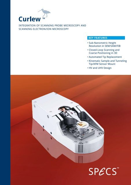
Curlew brochure - SPECS Surface Nano Analysis GmbH
Curlew brochure - SPECS Surface Nano Analysis GmbH
Curlew brochure - SPECS Surface Nano Analysis GmbH

You also want an ePaper? Increase the reach of your titles
YUMPU automatically turns print PDFs into web optimized ePapers that Google loves.
Integration of Scanning Probe Microscopy and<br />
Scanning Electron/Ion Microscopy<br />
Key Features<br />
• Sub-<strong>Nano</strong>metric Height<br />
Resolution in SEM/SAM/FIB<br />
• Closed-Loop Scanning and<br />
Coarse Positioning in 3D<br />
• Automated Tip Replacement<br />
• Kinematic Sample and Tunneling<br />
Tip/AFM Sensor Mount<br />
• HV and UHV Design
Innovation in surface Spectroscopy and<br />
microscopy systems<br />
<strong>SPECS</strong> leads the way in state-of-the-art<br />
technology for electron spectroscopy and<br />
scanning probe microscopy.<br />
<strong>SPECS</strong> <strong>Surface</strong> <strong>Nano</strong> <strong>Analysis</strong> <strong>GmbH</strong><br />
<strong>SPECS</strong> headquarters with more than 150<br />
employees is located in the center of Germany’s<br />
capital Berlin with subsidiaries in Switzerland<br />
(<strong>SPECS</strong> Zurich <strong>GmbH</strong>) and in the USA (<strong>SPECS</strong><br />
Inc.). To be close to our customers we have liason<br />
offices in France and Spain. Furthermore we<br />
are represented all over the globe by our sales<br />
partners.<br />
We are a team of scientists and engineers who<br />
dedicate their knowledge and experience to<br />
the development, design, and production of<br />
instruments for surface science, materials<br />
research, and nanotechnology for more than 25<br />
years.<br />
State-of-the-art scanning<br />
probe microscopy sytems<br />
Our key to success is know-how, experience,<br />
intensive contact with scientists from all over the<br />
world, customer orientation, and reliable quality<br />
control.<br />
Thus, we see ourselves as partner for systems<br />
and components for your research.<br />
<strong>Curlew</strong> SPM
<strong>Curlew</strong> SPM<br />
In Situ SPM<br />
The combination of Scanning Probe<br />
Microscopy and Scanning Electron/Auger/<br />
Focused Ion Beam Microscopy is the<br />
perfect complement of imaging speed and<br />
resolution from millimeter field of views<br />
down to the atomic scale.<br />
New Perspectives in Scanning<br />
Probe Microscopy<br />
Microscopy on Different Length<br />
Scales<br />
The <strong>Curlew</strong> in situ SPM provides the possibility<br />
of analysis, probing, and manipulation of the<br />
same sample feature by SPM and SEM/SAM/<br />
FIB techniques without the need for timeconsuming<br />
feature backtracking. Futhermore, it<br />
adds sub-nanometer height resolution and the<br />
ability to image insulating surfaces to SEM and<br />
FIB systems. The many electron-/ion-matter<br />
interaction signals providing spectroscopic and<br />
crystallographic surface information can be<br />
superimposed with SPM topography data. The<br />
<strong>Curlew</strong> in situ SPM gives new perspectives<br />
with respect to surface analysis, probing and<br />
manipulation at the nanometer scale.<br />
SEM/SAM/FIB Integration<br />
The <strong>Curlew</strong> is readily integrated upon the<br />
stage of virtually any SEM/SAM/FIB system and is<br />
compatible with systems operating at ultra-high<br />
vacuum, high vacuum as well as environmental<br />
conditions. In particular the SPM geometry<br />
enables integration with short working distance<br />
SEM/SAM/FIB optics. Standalone SEM/SAM/FIB<br />
imaging resolution and analytical performance<br />
remain uncompromised. For SAM integration<br />
a non-magnetic version of the <strong>Curlew</strong> SPM is<br />
ideally suited.<br />
Side view of <strong>Curlew</strong> SPM:<br />
Ideal for integration with<br />
short working distance<br />
SEM/SAM/FIB optics
Multiprobe Station<br />
The <strong>Curlew</strong> concept is also expandable to a<br />
multiprobe station permitting advanced SPM<br />
and probing experiments with multiple tips to<br />
be combined with SEM vision-controlled tip<br />
navigation.<br />
Sensor Types<br />
The <strong>Curlew</strong> SPM features a stiff sensor design<br />
based on a ceramic tip holder with conductive<br />
paths for tip/sensor contacting. Manipulation<br />
of tips and sensors is easy and safe. The <strong>Curlew</strong><br />
SPM accepts different kinds of electrical sensors<br />
including tunneling tips, Akiyama-Probes<br />
(<strong>Nano</strong>sensors) as well as quartz-based sensors,<br />
like the <strong>SPECS</strong> KolibriSensor. All sensors have a<br />
protruding tip that allows for direct SEM visioncontrolled<br />
tip/sensor positioning and control.<br />
Coarse Tip Positioning<br />
The tip is positioned laterally and vertically by<br />
inertial piezo-motors with integrated optical<br />
encoders for closed-loop operation. A compact<br />
parallel kinematic coarse positioning motor<br />
design reduces the mechanical loop from sample<br />
to tip leading to higher stiffness and lower<br />
sensitivity to mechanical vibrations compared to<br />
the conventional stacked motor-axes design.<br />
SPM Scanner<br />
The Z tip scanner and the flexure-based XY<br />
sample stage can be optionally equipped with<br />
capacitive sensors that ensure perfectly linearized<br />
and calibrated closed-loop SPM scanning.<br />
Tip/Sensor Mount<br />
Tips and sensors are rigidly mounted to a<br />
precise kinematic interface between the ceramic<br />
tip holder and the <strong>Curlew</strong> tip receptor. This<br />
ensures perfect stability as well as enhanced<br />
and reliable performance of oscillating sensors.<br />
The spring-loaded design of the receptor is<br />
completely non-magnetic with a weight of<br />
less than 2 g. Four contact springs provide the<br />
electronic connections to the sensor or tip.<br />
Coaxial cabling and shielding of the contacts<br />
up to the sensor/tip minimize cross-talk and<br />
interference from the environment.<br />
The <strong>Curlew</strong> SPM is<br />
available with different<br />
kinds of tips and sensors,<br />
like the Akiyama-Probe,<br />
a self-sensing and selfactuating<br />
quartz tuning<br />
fork based cantilever<br />
sensor (left) and tungsten<br />
or Pt/Ir tunneling tips<br />
(right). Additional sensors<br />
are available on request.<br />
<strong>Curlew</strong> SPM
Sample Mount<br />
5<br />
The sample holder is kinematically mounted on<br />
three ruby spheres in three radial grooves (Maxwell<br />
geometry). This assures a mechanically firm and<br />
perfectly defined position. Electrical biasing<br />
of the sample is available via shielded cables.<br />
Various sample holders can be installed in<br />
the <strong>Curlew</strong> sample receptor. The basic design<br />
provides an adapter for standard SEM pin stub<br />
holders for convenient mounting and storage of<br />
samples.<br />
Tip/Sensor Replacement<br />
The <strong>Curlew</strong> SPM features sample and tip/<br />
sensor replacement inside a UHV chamber or<br />
through a load-lock chamber using a transfer<br />
rod or a wobble stick. The automated tip/sensor<br />
replacement procedure is highly user-friendly<br />
and safe. The innovative design features tip<br />
mounting and unmounting without any friction<br />
from metallic springs or contacts.<br />
The kinematic sample<br />
receptor-mount of the<br />
<strong>Curlew</strong> SPM (top) enables<br />
tip/sensor replacement by<br />
means of a user-friendly<br />
tip/sensor transfer shuttle<br />
(bottom).
<strong>Nano</strong>nis SPM Control System<br />
The <strong>Nano</strong>nis Control System offers the highest<br />
resolution, lowest noise and the greatest<br />
flexibility in SPM. All SPM modes are available<br />
and the control system is readily expandable for<br />
multi-tip control.<br />
The <strong>Curlew</strong> Control System consists of:<br />
• <strong>Nano</strong>nis SPM Control System Base Package<br />
• <strong>Nano</strong>nis Oscillation Controller<br />
• FEMTO preamplifier kit<br />
• High voltage amplifier and controller for<br />
scanners<br />
• High voltage amplifier and controller for<br />
coarse approach motors<br />
Integration into Analytical<br />
Instruments<br />
Live Performance of <strong>Curlew</strong> SPM<br />
The <strong>Curlew</strong> is a compact and versatile SPM,<br />
enabling integration into almost any kind of SEM,<br />
SAM or FIB and even into many other analytical<br />
instruments like SIMS. Successful integration into<br />
Tescan and JEOL microscopes has already been<br />
proven.<br />
AFM height image (6 μm x 6 μm) of a calibration<br />
grating measured with an Akiyama-Probe sensor<br />
in FM-AFM mode. The height scale is blown up by<br />
20 times relative to the lateral scale. The data was<br />
acquired during a live demonstration at the M&M<br />
conference 2011 in Nashville, USA.<br />
20<br />
15<br />
Z[nm]<br />
10<br />
5<br />
-0<br />
-0<br />
1<br />
2<br />
3<br />
X[µm]<br />
4<br />
5<br />
6<br />
AFM height profile along the line indicated above.<br />
<strong>Curlew</strong> SPM
<strong>Curlew</strong> SPM Operated inside SEM<br />
Specifications<br />
7<br />
SEM images of Akiyama-Probe cantilever tip<br />
above patterned surface prepared by SEM e-beam<br />
lithography. The AFM tip is navigated to the region<br />
of interest by real-time SEM imaging.<br />
<strong>Curlew</strong> SPM Head<br />
XY Scan Range (Sample)<br />
Z Scan Range (Tip)<br />
XYZ Sensor Resolution<br />
(Closed-Loop Option)<br />
Coarse Tip Positioning<br />
Range<br />
Coarse Tip Positioning<br />
Min. Step Size<br />
Coarse Tip Positioning<br />
Absolute Accuracy<br />
UHV Compatibility<br />
10 μm x 10 μm,<br />
50 μm x 50 μm optional<br />
2 μm,<br />
8 μm optional<br />
< 100 pm rms<br />
@ 1 kHz BW<br />
± 5 mm (X,Y), 5 mm (Z)<br />
Approx. 30 nm<br />
± 5 μm<br />
Bakeout Temperature 120 °C<br />
Load-Lock Compatibility<br />
SPM Tip/Sensor<br />
Weight<br />
Temperature Control<br />
optional<br />
< 2 x 10 -9 mbar<br />
Sample and SPM tip/<br />
sensor replacement via<br />
load-lock<br />
Etched and cut metal<br />
wire tunneling tips.<br />
Quartz tuning fork based<br />
cantilever AFM sensor<br />
(Akiyama- Probe).<br />
Approx. 350 g<br />
Resistive heater and<br />
temperature sensor<br />
integrated in the SPM<br />
chassis.<br />
Separate temperature<br />
controller for thermal<br />
stabilization of SPM head<br />
at room-temperature.<br />
Customization is the key to its flexibility.<br />
Please discuss your individual needs with us.<br />
AFM topography data in the region of interest<br />
(4 μm x 4 μm) measured inside the SEM.<br />
Dimensions of standard <strong>Curlew</strong> SPM stage
<strong>SPECS</strong> <strong>Surface</strong> <strong>Nano</strong> <strong>Analysis</strong> <strong>GmbH</strong><br />
Voltastrasse 5<br />
13355 Berlin / Germany<br />
www.specs.com<br />
T +49 30 46 78 24-0<br />
F +49 30 46 42 083<br />
E support@specs.com