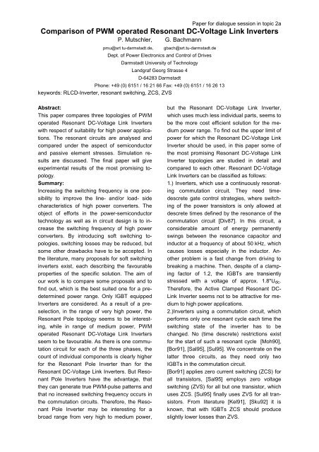
Comparison of PWM operated Resonant DC-Voltage Link Inverters
Comparison of PWM operated Resonant DC-Voltage Link Inverters
Comparison of PWM operated Resonant DC-Voltage Link Inverters

Create successful ePaper yourself
Turn your PDF publications into a flip-book with our unique Google optimized e-Paper software.
Paper for dialogue session in topic 2a<br />
<strong>Comparison</strong> <strong>of</strong> <strong>PWM</strong> <strong>operated</strong> <strong>Resonant</strong> <strong>DC</strong>-<strong>Voltage</strong> <strong>Link</strong> <strong>Inverters</strong><br />
P. Mutschler, G. Bachmann<br />
pmu@srt tu-darmstadt.de,<br />
gbach@srt.tu-darmstadt.de<br />
Dept. <strong>of</strong> Power Electronics and Control <strong>of</strong> Drives<br />
Darmstadt University <strong>of</strong> Technology<br />
Landgraf Georg Strasse 4<br />
D-64283 Darmstadt<br />
Phone: +49 (0) 6151 / 16 21 66 Fax: +49 (0) 6151 / 16 26 13<br />
keywords: RLCD-Inverter, resonant switching, ZCS, ZVS<br />
Abstract:<br />
This paper compares three topologies <strong>of</strong> <strong>PWM</strong><br />
<strong>operated</strong> <strong>Resonant</strong> <strong>DC</strong>-<strong>Voltage</strong> <strong>Link</strong> <strong>Inverters</strong><br />
with respect <strong>of</strong> suitability for high power applications.<br />
The resonant circuits are analysed and<br />
compared under the aspect <strong>of</strong> semiconductor<br />
and passive element stresses. Simulation results<br />
are discussed. The final paper will give<br />
experimental results <strong>of</strong> the most promising topology.<br />
Summary:<br />
Increasing the switching frequency is one possibility<br />
to improve the line- and/or load- side<br />
characteristics <strong>of</strong> high power converters. The<br />
object <strong>of</strong> efforts in the power-semiconductor<br />
technology as well as in circuit design is to increase<br />
the switching frequency <strong>of</strong> high power<br />
converters. By introducing s<strong>of</strong>t switching topologies,<br />
switching losses may be reduced, but<br />
some other drawbacks have to be accepted. In<br />
the literature, many proposals for s<strong>of</strong>t switching<br />
inverters exist, each describing the favourable<br />
properties <strong>of</strong> the specific solution. The aim <strong>of</strong><br />
our work is to compare some proposals and to<br />
find out, which is the best suited one for a predetermined<br />
power range. Only IGBT equipped<br />
<strong>Inverters</strong> are considered. As a result <strong>of</strong> a preselection,<br />
in the range <strong>of</strong> very high power, the<br />
<strong>Resonant</strong> Pole topology seems to be interesting,<br />
while in range <strong>of</strong> medium power, <strong>PWM</strong><br />
<strong>operated</strong> <strong>Resonant</strong> <strong>DC</strong>-<strong>Voltage</strong> <strong>Link</strong> <strong>Inverters</strong><br />
seem to be favourable. As there is one commutation<br />
circuit for each <strong>of</strong> the three phases, the<br />
count <strong>of</strong> individual components is clearly higher<br />
for the <strong>Resonant</strong> Pole Inverter than for the<br />
<strong>Resonant</strong> <strong>DC</strong>-<strong>Voltage</strong> <strong>Link</strong> <strong>Inverters</strong>. But <strong>Resonant</strong><br />
Pole <strong>Inverters</strong> have the advantage, that<br />
they can generate true <strong>PWM</strong>-pulse patterns and<br />
that no increased switching frequency occurs in<br />
the commutation circuits. Therefore, the <strong>Resonant</strong><br />
Pole Inverter may be interesting for a<br />
broad range from very high to medium power,<br />
but the <strong>Resonant</strong> <strong>DC</strong>-<strong>Voltage</strong> <strong>Link</strong> Inverter,<br />
which uses much less individual parts, seems to<br />
be the more cost efficient solution for the medium<br />
power range. To find out the upper limit <strong>of</strong><br />
power for which the <strong>Resonant</strong> <strong>DC</strong>-<strong>Voltage</strong> <strong>Link</strong><br />
Inverter should be used, in this paper some <strong>of</strong><br />
the most promising <strong>Resonant</strong> <strong>DC</strong>-<strong>Voltage</strong> <strong>Link</strong><br />
Inverter topologies are studied in detail and<br />
compared to each other. <strong>Resonant</strong> <strong>DC</strong>-<strong>Voltage</strong><br />
<strong>Link</strong> <strong>Inverters</strong> can be classified as follows:<br />
1.) <strong>Inverters</strong>, which use a continuously resonating<br />
commutation circuit. They need timedescrete<br />
gate control strategies, where switching<br />
<strong>of</strong> the power transistors is only allowed at<br />
descrete times defined by the resonance <strong>of</strong> the<br />
commutation circuit [Div87]. In this circuit, a<br />
considerable amount <strong>of</strong> energy permanently<br />
swings between the resonance capacitor and<br />
inductor at a frequency <strong>of</strong> about 50 kHz, which<br />
causes losses especially in the inductor. Another<br />
problem is a fast change from driving to<br />
breaking a machine. Then, despite <strong>of</strong> a clamping<br />
factor <strong>of</strong> 1.2, the IGBTs are transiently<br />
stressed with a voltage <strong>of</strong> approx. 1.8*U dc .<br />
Therefore, the Active Clamped <strong>Resonant</strong> <strong>DC</strong>-<br />
<strong>Link</strong> Inverter seems not to be attractive for medium<br />
to high power applications.<br />
2.)<strong>Inverters</strong> using a commutation circuit, which<br />
performs only one resonant cycle each time the<br />
switching state <strong>of</strong> the inverter has to be<br />
changed. No (time descrete) restrictions exist<br />
for the start <strong>of</strong> such a resonant cycle [Moh90],<br />
[Bor91], [Sal95], [Sul95]. We concentrate on the<br />
latter three circuits, as they need only two<br />
IGBTs in the commutation circuit.<br />
[Bor91] applies zero current switching (ZCS) for<br />
all transistors, [Sal95] employs zero voltage<br />
switching (ZVS) for all but one transistor, which<br />
uses ZCS. [Sul95] finally uses ZVS for all transistors.<br />
From literature [Kel91], [Sku92] it is<br />
known, that with IGBTs ZCS should produce<br />
slightly lower losses than ZVS.
At first, all three topologies have been simulated<br />
using ideal switches and the critical voltage- and<br />
current-stress on the devices has been pointed<br />
out. Then, some semiconductor effects like rise<br />
and fall time or tail current where taken into<br />
consideration in a simplified way. Finally, a teststand<br />
for the most promising solution is under<br />
construction now and measurements will be<br />
included in the final paper.<br />
D H<br />
U d<br />
2 T H<br />
T a Da 1 3 5<br />
C C<br />
U d<br />
2<br />
L C<br />
i L<br />
i C<br />
D r<br />
L di<br />
U C<br />
i Ldi<br />
Fig. 1: Circuit for ZCS for all IGBTs<br />
Figure 1 depicts a circuit, which realises ZCS<br />
for all IGBTs. Originally it was developed for<br />
GTO-<strong>Inverters</strong> with increased switching frequency.<br />
In the steady state the energy for the<br />
resonant operation is stored in the capacitor C C<br />
which is charged up to U d . The resonant cycle is<br />
triggered by turning on IGBT T a . A resonant<br />
oscillation determined by L C and C C starts. The<br />
resonant oscillation drives a current against the<br />
<strong>DC</strong>-link current so that D H starts conducting and<br />
T H can be turned <strong>of</strong>f under ZCS conditions. By<br />
this, the inverter bridge is separated from the<br />
<strong>DC</strong>-link. As soon as i Ldi has discharged C C to<br />
zero all IGBTs in the bridge are turned on and i L<br />
increases sinusoidal. When i L has passed its<br />
maximum and becomes negative the Diodes<br />
D 1 ..D 6 start conducting and the IGBTs can be<br />
turned <strong>of</strong>f under ZCS conditions. Finally when<br />
the current distribution in the bridge has<br />
reached its final state, the IGBT T H is turned on<br />
to charge C C to U d again. When u C reaches U d<br />
D r starts conducting to demagnetize L C. The<br />
new circuit state can be set while three diodes<br />
in the inverter bridge are conducting.<br />
L R<br />
T R<br />
D R<br />
1 3 5<br />
T C D C<br />
U d u B<br />
u C<br />
u CR<br />
C C<br />
C R<br />
Fig. 2: ZVS for most IGBTs [Sal98]<br />
2<br />
The circuit shown in Figure 2 provides ZVS for<br />
the IGBTs in the inverter-bridge and T c , T R is<br />
2<br />
4<br />
4<br />
6<br />
6<br />
M<br />
3~<br />
U d<br />
switched <strong>of</strong>f under ZCS conditions. The capacitors<br />
C C and C R are charged up to 1,2U d , the<br />
capacitance <strong>of</strong> C c is about 100 times C R . To<br />
trigger the resonant cycle the IGBTs in the<br />
resonant circuit T C and T R are turned on simultaneously,<br />
the voltage u B is clamped to the capacitor<br />
voltage u CR . A low frequency resonant<br />
oscillation determined by L R and C C starts.<br />
When i TC reaches the level I TP , the IGBT T C is<br />
turned <strong>of</strong>f, the current in T C commutates to C R<br />
and discharges it. When u B reaches zero the<br />
IGBTs in the bridge can be switched under ZVS<br />
conditions within a short period <strong>of</strong> time which is<br />
determined by the conducting state <strong>of</strong> the diodes<br />
D 1 ..D 6 . To restore the capacitor charge <strong>of</strong><br />
C R and C C both IGBTs <strong>of</strong> one inverter leg are<br />
turned on together for a short time which is<br />
determined by the charge flowed out the capacitor<br />
C C . When the new circuit state is set the<br />
capacitors C R and C C are charged up to 1,2U d<br />
again.<br />
T R1<br />
D R1<br />
T R2 D R2<br />
1 3 5<br />
D R4<br />
CR<br />
I 0<br />
U I0 /2<br />
C<br />
i L<br />
L<br />
Fig. 3: ZVS for all IGBTs [Sul95]<br />
2<br />
The resonant circuit introduced by Sul is shown<br />
in Figure 3. In the steady state the resonant<br />
tank energy is zero, T R1 is closed and T R2 is<br />
open. The snubber capacitors provide ZVS<br />
switch <strong>of</strong>f <strong>of</strong> the bridge IGBTs, independent <strong>of</strong><br />
the resonant circuit. By turning T R2 on, a resonant<br />
cycle is started. The current in T R1 increases<br />
to feed energy into the resonant tank.<br />
As soon as i L reaches I TP1 T R1 is opened and u B<br />
is clamped to the snubber capacitor voltage u C .<br />
i L then discharges the snubber capacitors.<br />
When u B reaches zero all the IGBTs in the inverter<br />
are turned on under ZVS conditions. i L<br />
changes its direction and when it reaches the<br />
negative value i TP2 the new circuit state is set.<br />
The snubber capacitors are charged up to U d<br />
and T R1 is turned on under ZVS conditions. C R<br />
is discharged via D R1 and D R2 . When u C<br />
reaches zero L is demagnetized via D R1 and<br />
D R4 .<br />
The circuits mentioned above have been simulated.<br />
Comparing the simulation results, we<br />
decided to build up an experimental set-up,<br />
based on [Sul95] for the following reasons:<br />
4<br />
6<br />
I 0<br />
/2
• An estimation on power losses in the resonant<br />
circuit during one resonant cycle shows,<br />
that due to rather long conducting times, the<br />
ZCS solution [Bor91] will produce higher<br />
losses than the ZVS solutions.<br />
• The voltage stress <strong>of</strong> semiconductors is in<br />
the circuit [Sal95] is higher than in [Sul95].<br />
• In order to achieve ZVS, an extreme precise<br />
gate timing seems to be necessary with<br />
[Sal95]. [Sul95] is less sensitive in this respect.<br />
• The snubber-capacitors allow a ZVS turn <strong>of</strong>f<br />
any time irrespective <strong>of</strong> the link voltage<br />
• In [Sul95] the IGBT T R1 can be used to separate<br />
the inverter-bridge from the <strong>DC</strong>-link in<br />
case <strong>of</strong> an fault.<br />
• In [Sul95] the resonant tank energy is stationary<br />
zero, so there is no need for controlling<br />
it<br />
• Overvoltages produced by parasitic inductances<br />
are damped by the snubber capacitors.<br />
1500V<br />
1000V<br />
500V<br />
1500V<br />
1000V<br />
500V<br />
1000A<br />
500A<br />
750A<br />
0A<br />
-750A<br />
0,0s 5,0µs 10,0µs 15,0µs<br />
600A<br />
400A<br />
200A<br />
600A<br />
400A<br />
200A<br />
600A<br />
400A<br />
200A<br />
600A<br />
400A<br />
200A<br />
600A<br />
400A<br />
200A<br />
I TP1<br />
u C<br />
5,0µs 10,0µs 15,0µs<br />
0,0s 5,0µs 10,0µs 15,0µs<br />
i TR1<br />
0,0s 5,0µs 10,0µs 15,0µs<br />
i T1<br />
i LR<br />
u B<br />
0,0 5,0µ 10,0µ 15,0µ<br />
i D2<br />
0,0 5,0µ 10,0µ 15,0µ<br />
i T4<br />
0,000000 0,000005 0,000010 0,000015<br />
i D4<br />
i D3<br />
0,000000 0,000005 0,000010 0,000015<br />
i D5<br />
i T4<br />
I TP2<br />
i T3<br />
i T5<br />
i D3<br />
i TR1<br />
i Dr4<br />
this example. This is a disadvantage <strong>of</strong> [Sul95],<br />
but this problem can be solved by using two<br />
parallel IGBTs to realise T R1 . The maximum<br />
current <strong>of</strong> the IGBTs 1-6 is close to the maximum<br />
load current.<br />
As long as (in the mentioned case) D 2 conducts<br />
the inverter bridge transistors can be switched<br />
under ZVS conditions. At the end <strong>of</strong> the resonant<br />
cycle the diode D R4 feeds the surplus <strong>of</strong><br />
resonant tank energy back into the <strong>DC</strong>-link.<br />
The final paper will present experimental results<br />
using a resonant circuit (1.5KV, 150A) according<br />
to [Sul95] and discuss the differences <strong>of</strong> the<br />
three circuits in more detail.<br />
References:<br />
[Bor91]<br />
[Div87]<br />
[Kel91]<br />
[Moh90<br />
]<br />
[Sal95]<br />
[Sku92]<br />
[Sul95]<br />
Bornhardt, K.: Neue GTO-Umrichter mit erhöhter<br />
Schaltfrequenz. PhD Thesis TH Darmstadt 1991<br />
Divan, D; Skibinski, G.: Zero Switching Loss<br />
<strong>Inverters</strong> For High Power Applications, IEEE-IAS<br />
Ann. Conference, 1987, p.. 627-634<br />
Keller, C.: Einsatzkriterien schneller abschaltbarer<br />
Leistungshalbleiter in Quasi-Resonanz-<br />
Umrichtern. PhD Thesis TU Berlin 1991<br />
Mohan, N.; He, J.; Wold, B.: Zero <strong>Voltage</strong><br />
Switching <strong>PWM</strong> Inverter For High -Frequency<br />
<strong>DC</strong>-AC Power Conversion. IEEE -IAS Annual<br />
Confrence 1990, p. 1215 - 1221<br />
Salama, S.; Tadros, Y.: Novel S<strong>of</strong>t Switching<br />
Quasi <strong>Resonant</strong> 3-Phase IGBT Inverter. EPE 95,<br />
Sevilla, p.. 2.095 -2.099<br />
Skudelny, H.; Protiwa, F.; Frey, T.: <strong>Comparison</strong><br />
<strong>of</strong> Different Switching Modes in a 10KW High<br />
Frequency Step Down Converter using IGBTs.<br />
IEEE Industry Applications Society Annual Meeting,<br />
1992, p. 964-96<br />
Sul, K.; Kim, J.: <strong>Resonant</strong> <strong>Link</strong> Bidirectional<br />
Power Converter: Part I- <strong>Resonant</strong> Circuit. IEEE<br />
Trans. on Power Electronics Vol. 10, No.4, July<br />
1995, p.. 479 - 484<br />
i DR1<br />
t 7<br />
0,000000 0,000005 0,000010 0,000015<br />
600A<br />
400A<br />
200A<br />
i T6<br />
i T6<br />
i D6<br />
t 0<br />
t 1<br />
t 2<br />
t 5<br />
t 2a<br />
t 3<br />
t 3a<br />
t 4<br />
t 6<br />
5,0µs 10,0µs 15,0µs<br />
Fig. 4: Commutation process in [Sul95]<br />
Figure 4 depicts the simulation results using the<br />
resonant circuit from Sul shown in figure 3. In<br />
this simulation a change from voltage-vector {1}<br />
to {2} is examined. The load-side currents are<br />
assumed to be constant for the time the resonant<br />
operation takes. The resonant operation is<br />
triggered at t 0 . At t 1 T R1 has to switch <strong>of</strong>f a current<br />
that is about two times the load-current in