INDUSTRY CHIEFS - DOPS - Danish Optical Society
INDUSTRY CHIEFS - DOPS - Danish Optical Society
INDUSTRY CHIEFS - DOPS - Danish Optical Society

You also want an ePaper? Increase the reach of your titles
YUMPU automatically turns print PDFs into web optimized ePapers that Google loves.
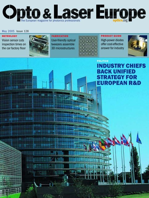
The European magazine for photonics professionals<br />
May 2005 Issue 128<br />
METROLOGY<br />
Vision sensor cuts<br />
inspection times on<br />
the car factory floor<br />
FABRICATION<br />
User-friendly optical<br />
tweezers assemble<br />
3D microstructures<br />
PRODUCT GUIDE<br />
High-power diodes<br />
offer cost-effective<br />
answer for industry<br />
POLITICS<br />
<strong>INDUSTRY</strong> <strong>CHIEFS</strong><br />
BACK UNIFIED<br />
STRATEGY FOR<br />
EUROPEAN R&D
Still milking your current<br />
optical software for all it’s worth?<br />
Get more with ASAP 2005.<br />
Bio-Optic Systems<br />
Coherent Systems<br />
Displays<br />
Imaging Systems<br />
Lightpipes<br />
Reflectors/Luminaires<br />
Stray Light Analysis<br />
<strong>Optical</strong> Software for<br />
Physicists and Engineers<br />
If you are at a dead end with your current optical software program,<br />
look no further than ASAP 2005. Twenty years of continuous<br />
development and commercial use allow ASAP 2005 to simulate<br />
the physics of more optical systems than any other software<br />
program available. With ASAP 2005, you get unmatched capability,<br />
flexibility, speed and accuracy—everything you need to create<br />
without compromise. Interoperable with popular CAD programs,<br />
including CATIA ® , SolidWorks ® and Rhinoceros ® , as well as<br />
the finite-difference code FDTD Solutions, ASAP 2005 lets you<br />
jump straight into the optical-modeling process. And since<br />
ASAP 2005 will model the finest details, you can depend on your<br />
simulation results to mirror real-world performance. Design better<br />
products and reduce your development timeline with ASAP 2005.<br />
ASAP 2005 <strong>Optical</strong> Modeling Software:<br />
Design | Model | Analyze<br />
Engineering | Software | Training<br />
ISO 9001:2000 Certified<br />
800.882.5085 USA|Canada<br />
1.520.721.0500 Worldwide
EDITORIAL<br />
Editor Oliver Graydon<br />
Tel: +44 (0)117 930 1015<br />
oliver.graydon@iop.org<br />
Technology editor Jacqueline Hewett<br />
Tel: +44 (0)117 930 1194<br />
jacqueline.hewett@iop.org<br />
Reporter James Tyrrell<br />
Tel: +44 (0)117 930 1256<br />
james.tyrrell@iop.org<br />
Production editors Lucy Farrar, Clare Sturges<br />
Technical illustrator Alison Tovey<br />
EUROPE/ROW SALES<br />
Advertising sales manager Rob Fisher<br />
Tel: +44 (0)117 930 1260<br />
robert.fisher@iop.org<br />
Key accounts manager Simon Allardice<br />
Tel: +44 (0)117 930 1284<br />
simon.allardice@iop.org<br />
Key accounts manager Adrian Chance<br />
Tel: +44 (0)117 930 1193<br />
adrian.chance@iop.org<br />
Sales executives Cadi Jones, Jo Hook<br />
Tel: +44 (0) 117 930 1090/1028<br />
cadi.jones@iop.org/jo.hook@iop.org<br />
US SALES OFFICE<br />
IOP Publishing Inc, Suite 929, 150 South<br />
Independence Mall West, Philadelphia PA 19106, USA<br />
Tel: +1 215 627 0880<br />
Fax: +1 215 627 0879<br />
ADVERTISING PRODUCTION<br />
Advertising production coordinator Teresa Honey<br />
Tel: +44 (0)117 930 1040<br />
teresa.honey@iop.org<br />
Advertising production editor Tanwen Haf<br />
CIRCULATION AND MARKETING<br />
Product manager Angela Peck<br />
Tel: +44 (0)117 930 1025<br />
angela.peck@iop.org<br />
ART DIRECTOR<br />
Andrew Giaquinto<br />
PUBLISHER<br />
Geraldine Pounsford<br />
Tel: +44 (0)117 930 1022<br />
geraldine.pounsford@iop.org<br />
PUBLISHING DIRECTOR<br />
Richard Roe<br />
OPTO & LASER EUROPE<br />
Dirac House,Temple Back,<br />
Bristol BS1 6BE, UK.<br />
Tel: +44 (0)117 929 7481<br />
Editorial fax: +44 (0)117 925 1942<br />
Advertising fax: +44 (0)117 930 1178<br />
Internet: optics.org/ole<br />
ISSN 0966-9809 CODEN OL EEEV<br />
SUBSCRIPTIONS<br />
Complimentary copies are sent to qualifying<br />
individuals (for more details see optics.org/ole/<br />
subscribe). For readers outside registration<br />
requirements: £111/€160 ($199 US and Canada)<br />
per year. Single issue £10/€14 ($18 US, Canada<br />
and Mexico). CONTACT: IOPP Magazines, WDIS Ltd,<br />
Units 12 & 13, Cranleigh Gardens Industrial Estate,<br />
Southall, Middlesex UB1 2DB, UK.<br />
Tel: +44 (0)208 606 7518. Fax: +44 (0)208 606 7303.<br />
E-mail: opto&lasereurope@iop.org<br />
© 2005 IOP Publishing Ltd. The contents of OLE do<br />
not represent the views or policies of the Institute of<br />
Physics, its council or its officers unless so identified.<br />
This magazine incorporates Opto & Laser Products.<br />
Printed by Warners (Midlands) plc, The Maltings,<br />
West Street, Bourne, Lincolnshire PE10 9PH, UK.<br />
Issue 128 May 2005<br />
Acquisitions continue in<br />
the world of optics p5<br />
Better beams: multimode<br />
lasers get a new look p17<br />
<strong>Optical</strong> manipulation gets<br />
user-friendly p26<br />
Keeping cool: a tutorial on<br />
laser-diode basics p31<br />
Cover The European<br />
Parliament building in<br />
Strasbourg, France. p23<br />
NEWS<br />
5 Business Consolidation and acquisition at JDSU•Innoled to<br />
trial OLED production•Giant kaleidoscope opens its doors<br />
9 Editorial Europe’s new challenge<br />
11 Analysis Cambridge Display Technology: braving the market<br />
TECHNOLOGY<br />
15 Applications High-res implant aids poor vision• Glasses-free<br />
3D goes the distance• Holography images live cells in 3D<br />
18 R&D Multimode lasers get brighter•Four-band camera aids<br />
IR study of the environment•Light locks plastics in position<br />
21 Patents Ceramic motors provide optics with silent answer<br />
FEATURES<br />
23 Photonics report advises new direction for EC<br />
Can European photonics remain competitive with firms in Asia<br />
and the US? Yes, but only if a new, unified approach to research<br />
is adopted, says the EPIC. Oliver Graydon reports.<br />
26 <strong>Optical</strong> manipulation plays trick with particles<br />
<strong>Danish</strong> scientists have harnessed the power of light beams to<br />
manipulate 3D arrangements of particles at the click of a mouse<br />
button. Rob van den Berg reports.<br />
29 <strong>Optical</strong> sensor helps to speed up car production<br />
French firm ActiCM’s high-speed, vision-based co-ordinate<br />
measuring machine is grabbing the attention of big names in<br />
the car industry. James Tyrrell finds out why.<br />
31 High-power diode lasers offer efficient answer<br />
High-power diode bars that are highly efficient and boast output<br />
powers of hundreds of watts are now commercially available.<br />
Merrill Apter gives a tutorial on the technology.<br />
SHOW PREVIEW<br />
22 The combined CLEO, QELS and PhAST conference comes to<br />
Baltimore, US, at the end of the month and has an<br />
action-packed programme ready for delegates.<br />
PRODUCTS<br />
37 Synthetic sapphire•MEMS motion analyser•Parabolic mirror<br />
REGULARS<br />
24 Free Literature/Search Engine<br />
49 People<br />
50 Calendar<br />
Contents<br />
For the latest news on optics and photonics don’t forget to visit optics.org
RESTRUCTURING<br />
NEWS<br />
BUSINESS 5 EDITORIAL 9 ANALYSIS 11<br />
Consolidation, acquisition at JDSU<br />
JDS Uniphase (JDSU), a provider of<br />
laser components and subsystems,<br />
has taken a bigger stake in the<br />
solid-state laser market by acquiring<br />
Lightwave Electronics for<br />
$65 m (750 m). By expanding into<br />
the mid- to high-power laser sector,<br />
JDSU hopes to broaden its customer<br />
base and grow its revenue.<br />
“We have seen an acceleration<br />
in the [solid-state laser] market,<br />
driven by a number of factors such<br />
as the demand for smaller-size,<br />
high-power lasers for portable and<br />
handheld devices,” JDSU director<br />
of communications Enzo Signore<br />
told OLE. “There is a big transition<br />
[taking place] as users migrate<br />
from gas-phase lasers to solid-state<br />
lasers, and Lightwave Electronics<br />
has expertise in this area.”<br />
Retaining their branding, Lightwave’s<br />
products will complement<br />
JDSU’s existing range that includes<br />
helium-neon and argon-ion gas<br />
lasers, industrial laser diodes, fibre<br />
Strategic move: JDSU purchases Lightwave and consolidates manufacturing.<br />
lasers and low-power solid-state<br />
lasers. The firm’s sources are used<br />
in a diverse range of applications<br />
in biotechnology, materials processing,<br />
remote sensing and semiconductor<br />
manufacturing.<br />
Lightwave’s 120 employees will<br />
move from its Mountain View site<br />
to the nearby JDSU facility in San<br />
Jose, California. The new business<br />
area will be led by Lightwave CEO<br />
Phillip Meredith and the acquisition<br />
is expected to complete in the<br />
second quarter of this year.<br />
Shortly after the news of the<br />
acquisition, JDSU announced that<br />
it was consolidating its North<br />
American manufacturing operations.<br />
By the end of the year the<br />
company expects to reduce its<br />
number of manufacturing positions<br />
by more than 15% (approximately<br />
850 staff).<br />
The consolidation will involve<br />
transferring production from the<br />
firm’s sites in New Jersey and<br />
Florida to its Shenzhen facility in<br />
China and to the facilities of two<br />
contract manufacturing partners.<br />
JDSU plans to reduce manufacturing<br />
in Santa Rosa, California, as<br />
it phases out some of its display<br />
products. The firm expects to complete<br />
the consolidation process by<br />
the end of the year.<br />
“These initiatives are part of<br />
JDSU’s business strategy to achieve<br />
profitability by reducing cost structure<br />
and improving corporate<br />
agility,” explained JDSU CEO Kevin<br />
Kennedy. “We firmly believe that<br />
our ability to restructure major<br />
operations and rationalize our current<br />
portfolio, while investing in<br />
next-generation products, positions<br />
JDSU for success.”<br />
ACQUISITIONS<br />
OmniVision completes purchase of CDM Optics<br />
OmniVision Technologies, a US<br />
supplier of CMOS image sensors<br />
for mobile phones and Web-cams,<br />
has acquired CDM Optics for<br />
$30 m (723 m). CDM has been<br />
successful in developing wavefront<br />
coding technology that substantially<br />
boosts camera performance<br />
by increasing the depth of field and<br />
correcting optical aberrations.<br />
“Currently, about 80% of Omni-<br />
Vision’s revenue comes from the<br />
camera cell-phone market and so<br />
our first goal is to adapt this technology<br />
to the camera cell-phone<br />
and digital-still camera market,”<br />
OmniVision CFO Peter Leigh told<br />
OLE. “Our objective as a company<br />
is to be the image sensor of choice<br />
in every end-use where an image<br />
sensor is required.” The Californian<br />
firm is keen to target emerging<br />
markets such as automotive, medical,<br />
security and surveillance.<br />
Competitive edge: CDM’s technology greatly expands the depth-of-field of an image.<br />
Images of MEMS and algae without (left) and with (right) wavefront coding.<br />
OmniVision feels that CDM’s<br />
expertise gives it a significant competitive<br />
advantage and so, rather<br />
than negotiating a licensing deal, it<br />
wanted to own the technology<br />
outright. “It means that each side<br />
can confidently share the technology<br />
it has with the other, without<br />
worrying about the possibility of<br />
undesirable disclosures to the outside<br />
world,” said Leigh.<br />
According to Leigh, the acquisition<br />
benefits both firms. “CDM were<br />
in a position where, to make this<br />
technology a reality, they needed<br />
more resources,” he said. “They<br />
decided they liked what OmniVision<br />
brought to the table and it made<br />
sense to join forces with a larger,<br />
more established company.” CDM’s<br />
18 employees will remain at its Colorado,<br />
US, location and the firm will<br />
operate as a wholly-owned subsidiary<br />
of OmniVision.<br />
OLE • May 2005 • optics.org<br />
5
NEWS<br />
BUSINESS<br />
DISPLAYS<br />
Innoled to trial OLED production<br />
By Manoj Aravindakshan<br />
in Singapore<br />
Singapore-based firm Innoled, a<br />
licensee of Cambridge Display<br />
Technology’s light-emitting polymer<br />
technology, is getting ready to<br />
commence pilot runs of its OLED<br />
production line, according to Peter<br />
Karlsson, Innoled’s managing<br />
director. Pilot production will start<br />
later this month in the Netherlands<br />
at the facilities of the company’s<br />
display equipment provider,<br />
OTB Engineering.<br />
“The pilot production will aim to<br />
improve yield from the processes,<br />
and produce some engineering<br />
samples for our customers,” said<br />
Karlsson. “We want to ensure that<br />
we have sorted out the yield before<br />
we move the production line to<br />
GIANT OPTICS<br />
Giant kaleidoscope<br />
opens its doors<br />
The world’s largest optical kaleidoscope<br />
has been constructed in<br />
Japan as a permanent exhibit at the<br />
2005 World Expo that is currently<br />
taking place near Nagoya.<br />
Officially opened on 25 March,<br />
the so-called “Earth Tower” consists<br />
of a 47 m-high triangular<br />
tower housing a set of mirrored<br />
surfaces and three gigantic revolving<br />
discs. Sunlight entering the<br />
building interacts with the moving<br />
Innoled is about to commence pilot<br />
production of its OLED displays, which<br />
are based on technology licensed from<br />
Cambridge Display Technology.<br />
Singapore.” This should happen by<br />
the end of this year, Karlsson added.<br />
The products will be marketed<br />
under the Nuovio brand-name.<br />
At full capacity, with a tack time<br />
discs and mirrors to produce a constantly<br />
changing 40 m-diameter<br />
Cambridge Display Technology<br />
Library<br />
of approximately 2 min and using<br />
a 14 × 14 inch glass substrate, the<br />
production line should be able to<br />
produce about 1.5 million mobilephone<br />
displays. Innoled is starting<br />
off with 1.7-inch monochrome<br />
displays with a resolution of<br />
128 × 64 pixels, but plans to be<br />
making active-matrix full-colour<br />
displays by 2007.<br />
Karlsson predicts that 2005/6<br />
will see the commercial breakthrough<br />
for OLEDs. “The second<br />
half of last year witnessed lots of<br />
MP3 players coming out with<br />
OLED displays, and many more<br />
applications are beginning to use<br />
OLEDs,” he noted.<br />
“A lot of work is being done to<br />
improve the energy-efficiency and<br />
lifetime of the display, but it will be<br />
A view of a typically beautiful pattern generated by the kaleidoscope (left) and the<br />
distinctive 47 m-high Earth Tower, which houses the optics.<br />
spherical image with stunning<br />
colours and shapes. The image is<br />
some time before we can see OLED<br />
displays for televisions or computers.<br />
The automotive sector will be a<br />
big market in the future, not only<br />
because of the higher brightness<br />
that OLEDs offer, but also due to<br />
their ability to withstand temperature<br />
variations, especially the cold.”<br />
Innoled is a joint venture<br />
between Eastgate Technology and<br />
Inline Display Technologies Europe<br />
BV of the Netherlands, with Eastgate<br />
holding a 70 percent stake.<br />
The fledgling unit received about<br />
$7.5 m (75.6 m) in funding from a<br />
local financial institution in<br />
November last year.<br />
Manoj Aravindakshan is director of<br />
On Target Media, a Singapore-based<br />
provider of technology news.<br />
viewed by observers from inside<br />
the base of the tower.<br />
The exhibit, which is Nagoya<br />
City’s contribution to the Expo, has<br />
already been accredited by Guinness<br />
World Records and has proved<br />
to be a big hit at the event, resulting<br />
in long queues of curious visitors.<br />
Fumiya Fuji, the designer of the<br />
Earth Tower, hopes that it will<br />
create feelings of serenity and<br />
tenderness in observers.<br />
The World Expo takes place in<br />
Aichi, Japan, and runs until 25<br />
September 2005.<br />
6 OLE • May 2005 • optics.org
NEWS<br />
BUSINESS<br />
IN BRIEF<br />
LICENSING<br />
US-based Universal Display<br />
Corporation (UDC) has licensed its<br />
organic LED technology to Samsung<br />
SDI of South Korea. The agreement<br />
allows Samsung to introduce UDC’s<br />
phosphorescent materials into its<br />
active-matrix OLED products. These<br />
materials have been shown to be<br />
up to four times more efficient than<br />
traditional fluorescent OLEDs,<br />
enabling lower power-consumption.<br />
FACILITIES<br />
Tinsley Industries has opened a<br />
new 30 000 sq. ft facility in<br />
Richmond, California, to grind and<br />
polish large mirror segments for the<br />
James Webb Space Telescope<br />
(JWST). The facility will be equipped<br />
with nine specially designed<br />
computer-controlled polishing<br />
machines and is expected to<br />
process all 18 of the JWST’s mirror<br />
segments in about 2.5 years.<br />
RESTRUCTURING<br />
Newport is divesting its loss-making<br />
robotic systems operations in<br />
Richmond, California, in order to<br />
concentrate on its core business of<br />
photonics. The business represents<br />
less than 5% of Newport’s net sales<br />
and is expected to lose $2.5–3.5 m<br />
in the first quarter of 2005.<br />
MARKETS<br />
Optoelectronics market to<br />
see strong growth to 2008<br />
The worldwide market for semiconductor<br />
optoelectronic components<br />
is predicted to increase at a<br />
growth rate of 20 percent, from<br />
$9 bn (77 bn) in 2003 to more<br />
than $22.3 bn by 2008, according<br />
to a report just published by Reed<br />
Electronics Research, UK. “Optoelectronics<br />
– a strategic study of<br />
the worldwide semiconductor<br />
optoelectronic component industry<br />
to 2008” is now in its third<br />
edition and deals with lasers, LEDs,<br />
detectors, image sensors, optocouplers<br />
and solar cells.<br />
“The business has changed considerably<br />
[since compiling the last<br />
report] and telecoms is now firmly<br />
seeded in second and maybe third<br />
place after, notably, data-storage<br />
and illumination and status indication,”<br />
analyst Roy Szweda told<br />
OLE. “Thanks to the development<br />
of the gallium nitride LED, there<br />
has been a huge increase in not<br />
just the use of coloured LEDs for<br />
backlighting in handsets, but also<br />
in white LEDs, particularly in<br />
architectural applications.”<br />
The market for LEDs of all types<br />
Money-spinner: the optoelectronics market is forecast to show strong and<br />
sustained growth through to 2008, thanks to booming sales of all types of LEDs.<br />
will continue to see some of the<br />
best growth in the opto market.<br />
The growth rate is forecast at<br />
23 percent from a 2003 market of<br />
$3.5 bn to $9.9 bn by 2008.<br />
Although the optical communications<br />
sector is experiencing a<br />
recovery, the opto market is going<br />
to continue to be dominated by<br />
applications outside the fibre sector,<br />
believes Szweda. Sales of new<br />
devices such as the violet laser,<br />
which will be used in next-generation<br />
DVD recorders, are likely to do<br />
well, but not until the arrival of<br />
high-definition television.<br />
“The device hasn’t yet got a grip<br />
on the data-storage market,” said<br />
Szweda. “The longer-wavelength<br />
red DVD doesn’t seem to want to lie<br />
down and stay still and we are continually<br />
seeing more and more<br />
capacity in the standard disk.”<br />
The report is available from Reed<br />
at a price of 71878 (book only) or<br />
72088 (book and CD-ROM).<br />
OLE • May 2005 • optics.org<br />
7
Prolite ® Laser Diodes… Also built to last.<br />
For applications requiring on/off operation like direct diode processing or<br />
pumping high power kW lasers, high power ProLite ® laser diodes from<br />
Spectra-Physics, a division of Newport, set a new lifetime standard. Today’s<br />
high power devices face internal stress from temperature cycling that can<br />
limit laser reliability, but you no longer have to settle for poor reliability.<br />
To offer our customers the longest lifetimes, we have<br />
made significant innovations in every aspect of process,<br />
materials and assembly. These improvements in epi<br />
quality, facet coating, moisture-resistant packaging,<br />
cooling and burn-in procedures allow us to offer<br />
reliability for on/off operation that rivals the long<br />
lifetimes we’ve always offered for CW use. In fact, we<br />
have the longest lifetimes in the industry.<br />
ProLite ® lasers are available from 800 nm to 980 nm, as single emitters, bars<br />
up to 50 Watts and multi-bar modules up to kilowatts of power, and with a<br />
wide range of packaging and output options. For lasers built to last, visit<br />
www. spectra-physics.com or call your local Newport or Spectra-Physics<br />
sales office. Contact addresses at www.newport.com/contactus<br />
In 2004 Spectra-Physics including Oriel Instruments, Richardson<br />
Gratings, Corion Filters and Hilger Crystals was acquired by Newport.<br />
©2004 Newport Corporation<br />
AD-040505-EN
NEWS<br />
EDITORIAL<br />
Ability<br />
Europe’s new challenge<br />
“European<br />
photonics<br />
needs to<br />
adopt a<br />
unified<br />
approach.”<br />
Oliver Graydon<br />
How the European photonics industry and its<br />
research can remain competitive with the US<br />
and Asia is an important question. You need<br />
only look at the situation in China to realize<br />
the scale of the issue.<br />
While the region has historically been<br />
viewed as a place with low manufacturing<br />
costs and little technology of its own, this<br />
situation will not persist indefinitely. Many<br />
foreign firms, including European ones, are<br />
currently benefiting from China’s abundant<br />
pool of cheap labour, but it is clear that the<br />
country’s own domestic firms and research<br />
centres are becoming more competitive.<br />
Several European associations are so<br />
concerned about the situation that they have<br />
put pen to paper and prepared a report for the<br />
European Commission (EC) advising it on how<br />
to strengthen Europe’s position (see p23).<br />
The report “Photonics for the 21st century<br />
– a consolidated European photonics research<br />
initiative” was compiled over a 12-month<br />
period by the European Photonics Industry<br />
Consortium (EPIC) and the Association of<br />
German Engineers (VDI). More than 60 big<br />
names in the optics sector, including the<br />
CEOs/CTOs of Aixtron, Carl Zeiss, Linos,<br />
Bookham and Rofin Sinar Laser, and the<br />
directors of several prestigious research<br />
institutes have given it their backing.<br />
EPIC and VDI’s report suggests that<br />
European photonics needs to adopt a unified<br />
approach to research in order to achieve the<br />
scale and capabilities required to remain<br />
competitive with the US and Asia. One of the<br />
key problems they highlight is the fragmented<br />
nature of European photonics – research being<br />
spread across countries and a diverse range of<br />
applications. A further complication is that the<br />
EU industrial base is mainly composed of SMEs,<br />
which have limited resources.<br />
The solution the authors propose is the<br />
creation of a unifying platform for photonics<br />
research that will help to improve strategic<br />
links between relevant parties. The proposal<br />
has now been put to the EC, and EPIC says it<br />
is waiting for a response to see if it will be<br />
adopted. It’s too early to be sure of the<br />
chances of success, but OLE will keep you<br />
updated as news becomes available. Until<br />
then, perhaps its best to keep your fingers<br />
crossed and hope that European photonics<br />
gets the investment it truly deserves.<br />
Oliver Graydon, editor<br />
E-mail: oliver.graydon@iop.org<br />
to Adapt<br />
Silicon Photodiodes<br />
Basic devices today, that have evolved<br />
and adapted to the ever-increasing application<br />
demands on performance and reliability.<br />
Large sizes available, up to a full wafer. Features<br />
include deep UV sensitivity and reliability, even<br />
at high power, high QE at wavelengths up to<br />
1000nm and sensitivity down to the fW level.<br />
Hybrid structures with amplifiers or APD’s with<br />
internal gain, filters and lenses on photodiodes,<br />
arrays and a flexible packaging technology.<br />
These are the key to high performance devices<br />
or sensors for low cost mass production.<br />
We adapt – now and in the future.<br />
Visit www.sales.hamamatsu.com to find<br />
the optimum solution for your application.<br />
S8594<br />
Quadrant photodiodes with<br />
slit mask, line/space = 10/10µm,<br />
for encoder<br />
S9345<br />
Dual element photodiode<br />
in an extremely thin,<br />
0.95 mm package<br />
S9270<br />
Large silicon photodiode<br />
with integrated amplifier,<br />
resistor and capacitor.<br />
PHOTON IS OUR BUSINESS<br />
Freephone:<br />
Europe 00 800 800 800 88<br />
USA 1-800 524 0504<br />
www.sales.hamamatsu.com<br />
OLE • May 2005 • optics.org<br />
9
NEWS<br />
ANALYSIS<br />
DISPLAYS<br />
OLED firm braves stock market<br />
Can a high-tech company create a profitable business by licensing technology and reaping the<br />
royalties? Robert Thomas investigates one such company having mixed results with this approach.<br />
CDT<br />
CDT has dramatically improved the brightness and lifetime of LEP materials over the past few years, but investors are not rushing to buy shares in the firm.<br />
Cambridge Display Technology<br />
(CDT), based in Cambridge, UK, is<br />
a pioneer and leading source of<br />
light-emitting polymer (LEP) technology.<br />
CDT became a public company<br />
in December 2004 and its<br />
stock now trades on the NASDAQ<br />
National Market under the ticker<br />
symbol “OLED” (organic lightemitting<br />
diodes).<br />
CDT’s LEPs are an essential<br />
component of polymer OLED displays<br />
– a next-generation display<br />
technology which, it is hoped, will<br />
challenge the dominance of LCDs.<br />
However, investor response to<br />
CDT’s initial public offering (IPO)<br />
has been distinctly lukewarm.<br />
Share price has fallen from a<br />
high of around $12 (79) on the<br />
day of the IPO, to a low of around<br />
$6 in early February. The stock<br />
recovered steadily in March – to<br />
the $8–9 range – but has since<br />
dropped to around $6 as OLE goes<br />
to press in mid-April.<br />
This lacklustre stock performance<br />
seems to reflect investor discomfort<br />
with CDT’s business model,<br />
Licensees of CDT’s LEP technology<br />
Type of licence<br />
Display devices<br />
Materials<br />
Semiconductor driver<br />
circuits<br />
possible concerns over its financial<br />
performance to date and misgivings<br />
about the prospects for its technology.<br />
Unlike most firms, CDT does<br />
not actually manufacture products;<br />
it generates revenues by licensing<br />
patented LEP technology.<br />
The company sold its first<br />
licence to Philips in 1996 and, by<br />
the end of 2004, had sold a total of<br />
Company<br />
Dai Nippon Printing<br />
Delta Optoelectronics<br />
DuPont Displays<br />
Innoled<br />
MicroEmissive Displays<br />
OSRAM Opto Semiconductors<br />
Royal Philips Electronics<br />
Covion Organic Semiconductors<br />
Dow Chemical<br />
H C Starck<br />
Sumitomo Chemical<br />
Plastic Logic<br />
STMicroelectronics<br />
14 licences to several leading displays<br />
producers (see table, above).<br />
In 2003, 10 licences accounted for<br />
74% of the firm’s revenue, but last<br />
year, just five licences accounted<br />
for 66% of revenues.<br />
CDT currently has 179 patents<br />
that have either been granted or<br />
are in the application process. Last<br />
year, it filed 34 new applications<br />
and was issued a total of 45 new<br />
patents. However, the revenue<br />
stream from licensing fees (typically<br />
a large one-off fee that the<br />
licensee pays up front) and royalties<br />
(a smaller ongoing fee) can be<br />
irregular and volatile.<br />
During 2001, CDT signed three<br />
licences and achieved record revenues<br />
of $22.4 m. But, in 2002, the<br />
company signed just one licensing<br />
agreement and, consequently, revenue<br />
dropped to $7.1 m.<br />
Since then, CDT’s annual revenues<br />
appear to be climbing again<br />
($10.7 m in 2003 and $13.3 m in<br />
2004), but its operating losses show<br />
no sign of decreasing ($31.2 m in<br />
2003 and $34.5 m in 2004). The<br />
result is that the firm is still a long<br />
way from reaching breakeven (with<br />
net losses of $22.8 m in 2003 and<br />
$34.8 m in 2004).<br />
The company’s annual report<br />
for 2004, filed with the US Securities<br />
and Exchange Commission<br />
(SEC), summarizes the situation<br />
bluntly: “We have a history of<br />
losses, do not expect to be<br />
▲<br />
OLE • May 2005 • optics.org<br />
11
eagleyard Photonics<br />
Excellent Team Player for<br />
Sophisticated Applications<br />
Distributed Feedback Lasers (DFB)<br />
Fabry Perot single mode lasers with integrated grating<br />
structure. Outstanding results due to top parameters:<br />
- stable and precise wavelengths<br />
from 763 to 1083 nm<br />
- extremely narrow linewidth < 5 MHz<br />
- output powers from 50 to 150 mW<br />
Applications in industry and science:<br />
fiber testing | analytics | Raman spectroscopy | frequency conversion |<br />
exciting atom resonances (e.g. RbCs)<br />
www.eagleyard.com<br />
We focus on power.
NEWS<br />
ANALYSIS<br />
Improvements in LEP lifetime (h)<br />
End 2000 End 2002 October 2004<br />
Red >40 000 >40 000 >210 000<br />
Green >10 000 >25 000 >260 000<br />
Blue >1900 >11 000 >80 000<br />
Yellow >5000 >30 000 >290 000<br />
Orange >10 000 >10 000 >320 000<br />
Lifetime is measured as the time to half-brightness from an initial brightness,<br />
then extrapolated to give predicted levels at 100 cd/m 2 .<br />
profitable in the foreseeable future<br />
and may never be.”<br />
One of the problems facing CDT<br />
is that its polymer OLED technology<br />
competes with tried-andtested<br />
LCDs, which are firmly<br />
entrenched in the market, and<br />
rival emerging technologies such<br />
as Eastman Kodak’s smallmolecule<br />
OLED technology. Business<br />
analysts have expressed<br />
scepticism regarding the ability of<br />
polymer OLED technology to make<br />
headway against this competition.<br />
CDT’s stock may also be a victim<br />
of bad timing. Many analysts categorized<br />
CDT as a nanotechnology<br />
player and drew parallels with<br />
Nanosys – the Californian start-up<br />
that attracted intense and unflattering<br />
media attention when it<br />
cancelled its IPO in August 2004,<br />
a few days after CDT announced<br />
its plans to go public.<br />
At present, investors seem to<br />
have little enthusiasm for nanotechnology<br />
stocks: the Merrill<br />
Lynch Nanotech Index and the<br />
Punk Ziegel Nanotechnology Index<br />
both declined in 2004 and neither<br />
has improved in 2005.<br />
CDT’s 2004 annual report<br />
describes its investment risks in<br />
some detail and gives an overview<br />
of the company’s financial performance<br />
to date. Much of the information<br />
is enough to make potential<br />
investors pause for thought, but<br />
also provides some grounds for<br />
optimism about CDT.<br />
Commercial products<br />
Several commercial products containing<br />
small monochrome displays<br />
based on CDT’s licensed OLED<br />
technology have already entered<br />
the market, including a mobile<br />
phone and an electric shaver by<br />
Philips, plus an MP3 player with a<br />
Delta Optoelectronics display.<br />
What’s more, CDT’s progress in<br />
significantly extending the lifetime<br />
of green, red, blue, orange and yellow<br />
LEPs could also mean that fullcolour<br />
commercial displays may<br />
not be far behind (see table, left).<br />
A number of CDT’s licensees<br />
have already demonstrated larger,<br />
full-colour displays using polymer-<br />
OLED technology. Recent demonstrations<br />
include 40 and 12.5 inch<br />
displays by Seiko Epson and a<br />
13 inch display by Philips.<br />
If polymer OLED technology is<br />
successful, CDT and its shareholders<br />
will be the lucky beneficiaries.<br />
At present, however, investors seem<br />
to be more wary of the risks associated<br />
with CDT’s stock than excited<br />
about the potential rewards. ■<br />
Robert Thomas is principal at SRI<br />
Consulting Business Intelligence, a<br />
business and technology research<br />
consultancy spin-off<br />
from the former<br />
Stanford Research<br />
Institute. See www.<br />
sric-bi.com or e-mail<br />
rthomas@sric-bi.com.<br />
OLE • May 2005 • optics.org<br />
13
CUSTOM LASIRIS LASERS<br />
For machine vision, inspection,<br />
and alignment<br />
MFL MICRO-FOCUS LASER<br />
• 3.0 micron line, FWHM<br />
• Ideal for precision inspection<br />
All laser models<br />
can be customized<br />
to meet your<br />
specific requirements.<br />
This includes<br />
altering the optical,<br />
electrical, and/or<br />
mechanical<br />
components.<br />
For a list of our distributors,<br />
please visit our website:<br />
www.stockeryale.com<br />
TEC LASER<br />
• Thermo-electrically cooled<br />
• Exceptional wavelength stability<br />
SNF LASER<br />
• Choose wavelength, power<br />
and pattern<br />
• Two-year warranty<br />
MAGNUM LASER<br />
• High power line generator<br />
• Robust design<br />
Celebrating 20 years<br />
in lasers and beam shaping!<br />
StockerYale Inc.<br />
275 Kesmark, Montreal, Quebec<br />
H9B 3J1 Canada<br />
Tel.: (514) 685-1005<br />
Fax: (514) 685-3307<br />
lasers@stockeryale.com<br />
NASDAQ: STKR<br />
Copyright ©2005 StockerYale, Inc. All rights reserved.
TECHNOLOGY<br />
APPLICATIONS 15 R&D 17 PATENTS 21<br />
VISION<br />
Hi-res implant aids poor vision<br />
By Oliver Graydon<br />
An artificial vision system with an<br />
imaging performance allegedly<br />
good enough to recognize faces,<br />
read large fonts and watch TV has<br />
been designed by a team of scientists<br />
at Stanford University, US.<br />
The system, described in a recent<br />
issue of the Journal of Neural Engineering,<br />
features a wallet-sized computer,<br />
a tiny video camera mounted<br />
on a pair of goggles and an infraredsensitive<br />
detector chip implanted in<br />
the retina. Tests are currently ongoing<br />
in rats, and the retinal chips are<br />
soon to be implanted in pigs. However,<br />
human trials are said to be at<br />
least three years away.<br />
The hope is that the system may<br />
one day be used improve the vision<br />
of people who suffer from retinal<br />
degeneration: the death of the<br />
eye’s photoreceptor cells. Around<br />
700 000 people each year are<br />
diagnosed with age-related macular<br />
degeneration, which results in<br />
impaired vision and, in some cases,<br />
complete blindness.<br />
DISPLAYS<br />
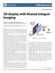
Glasses-free 3D<br />
goes the distance<br />
A 3D display that does not require<br />
special viewing spectacles could<br />
benefit television, computer gaming<br />
and even air-traffic control, say<br />
its Japanese inventors. Based on an<br />
array of small lenses, the device<br />
generates a 3D image, which has a<br />
perceived depth of several metres,<br />
for viewing with the naked eye<br />
(Optics Letters 30 613).<br />
The display uses so-called “integral<br />
photography” to generate its<br />
3D images. A computer divides<br />
the image into pixels that are<br />
either printed on photographic<br />
film or shown on a flat-screen display.<br />
When passed through an<br />
array of lenses, the result is a 3D<br />
image with a depth of 5.7 m or<br />
more in front of the display, and<br />
3.5 m or more behind it.<br />
OLE • May 2005 • optics.org<br />
Stanford University<br />
University of Tokyo, Japan<br />
Eyeing up the situation: Daniel Palanker and his team from Stanford University.<br />
In the past, difficulties in achieving<br />
the necessary proximity of a few<br />
micrometres between cells and<br />
electrodes severely limited the resolution<br />
of chip implants, resulting in<br />
poor vision. But the Stanford team’s<br />
chip enables users to perceive a 10°<br />
visual field at a good resolution.<br />
The system’s camera captures<br />
an image of a scene, which is<br />
“The integral photography technique<br />
has none of the inherent eyestraining<br />
problems associated with<br />
the continuous viewing of binocular<br />
stereoscopic displays,” University<br />
of Tokyo scientist Hongen Liao<br />
told OLE. “It is an ideal way to display<br />
autostereoscopic images.”<br />
Until now, the success of the<br />
passed to the computer for processing.<br />
An LCD illuminated with an<br />
infrared LED then projects an<br />
infrared image of the processed<br />
data through the eye onto a retinal<br />
chip, which stimulates nerve cells.<br />
The 3 mm 2 chip consists of a dense<br />
array of imaging pixels – infrared<br />
photodiodes connected to cellstimulating<br />
electrodes.<br />
Floating image: the letter ‘A’ appears in mid-air approximately 1 m from the screen.<br />
technique has been limited by the<br />
accuracy of the lens array, which<br />
is composed of glass lenslets of<br />
6 mm in diameter arranged in a<br />
35 × 35 hexagonal layout. But, as<br />
Liao explains, even a small error<br />
in the lens’s arrangement can<br />
cause image overlap and blurring,<br />
which limits the precision and<br />
The scientists say that the chip<br />
offers a resolution of 2500 pixels<br />
per millimetre, corresponding to a<br />
visual acuity of 20/80 – sufficient<br />
for reading a book or using a computer.<br />
The chip achieves this performance<br />
by letting cells grow around<br />
the electrodes, which either protrude<br />
from the chip like miniature<br />
pillars or are recessed into pores.<br />
“We actually invite cells to come<br />
to the electrode site, and they do it<br />
happily and very quickly,” said<br />
Stanford’s Daniel Palanker. Within<br />
three days, cells migrate to fill the<br />
spaces between the pillars and<br />
pores of the subretinal implant.<br />
Although other research teams<br />
in Germany, the US and Japan are<br />
also working on the topic, the Stanford<br />
approach uses a projection and<br />
tracking system to follow the rapid<br />
small movements the eye makes<br />
when viewing a scene. “In reality,<br />
when you think that you are staring<br />
at a certain point, your eyes are<br />
not steady,” said Palanker. “You are<br />
microscanning it all the time.”<br />
depth of the 3D image.<br />
“Most of the autostereoscopic<br />
displays only have an image depth<br />
of several centimetres,” said Liao.<br />
“To the best of our knowledge,<br />
there have been no reports about<br />
producing an image with a depth<br />
of several metres.”<br />
Liao and his colleagues have<br />
found a way of preparing images<br />
so that they can be viewed longdistance.<br />
Firstly, a computer pixelates<br />
the image to match the 3D<br />
display’s lens array and projects<br />
this image onto a screen.<br />
Next, the researchers use the<br />
lens array to capture the view on<br />
photographic film, creating a reference<br />
image that self-compensates<br />
for any lens distortion or<br />
misplacement. “Our method<br />
enables a display device to present<br />
deviation-free, distortion-free 3D<br />
images,” commented Liao. “We<br />
are now developing an animated<br />
integral videography device.”<br />
15
TECHNOLOGY<br />
APPLICATIONS<br />
MICROSCOPY<br />
Holography images live cells in 3D<br />
Swiss scientists have used a digital<br />
holographic microscope (DHM) to<br />
capture 3D phase images of transparent<br />
living cells. The team put its<br />
system to the test by imaging a living<br />
mouse neuron with an axial<br />
accuracy in the 160–320 nm<br />
range (Optics Letters 30 468).<br />
The researchers from the University<br />
of Lausanne and Ecole<br />
Polytechnique Fédérale de Lausanne<br />
(EPFL) have patented their<br />
technique and formed a company,<br />
Lyncée Tec, to market and manufacture<br />
DHM imaging systems.<br />
The Swiss group’s device is<br />
based around a Mach-Zehnder<br />
interferometer, with a 10 mW<br />
helium–neon laser (633 nm) providing<br />
the coherent light source.<br />
The big benefit of the technique is<br />
that it is able to focus on different<br />
object planes without using any<br />
optomechanical movement.<br />
“Digital processing replaces the<br />
ILLUMINATION<br />
High-brightness<br />
LEDs challenge<br />
car-lamp systems<br />
Lumileds, the Californian developer<br />
of high-brightness LEDs,<br />
claims to have developed a range of<br />
record-breaking devices that provide<br />
three times the lumen output<br />
of its best previous products.<br />
The new red, red-orange and<br />
amber Luxeon III LEDs emit 140,<br />
190 and 110 lm respectively and<br />
offer a lifetime (50% drop in<br />
lumen output) of 20 000 h when<br />
Lyncée Tec<br />
driven at 1400 mA.<br />
“This is a huge milestone for the<br />
automotive industry because, at<br />
these levels of performance, it<br />
enables manufacturers to meet the<br />
standards for rear-combination<br />
lamps [an optical unit featuring<br />
tail, brake and indicator light] with<br />
a single LED,” explained Steve Landau<br />
from Lumileds.<br />
“And because you move to a single<br />
LED solution, you start to have<br />
cost parity with a lamp system,” he<br />
continued. “That means you can<br />
implement the technology on a<br />
broader range of vehicles.”<br />
Aside from the automotive<br />
Lumileds University of Lausanne and EPFL<br />
The Swiss firm Lyncée Tec has been founded to commercialize and manufacture the<br />
DHM (left). A 3D DHM image of a living mouse cortical neuron in culture (right).<br />
need for complex optical adjustment<br />
procedures and allows [us] to<br />
correct lens aberrations introduced<br />
by the microscope objective,”<br />
research scientist Pierre<br />
Marquet told OLE. “[It can also]<br />
simulate the effect of optical components<br />
such as lenses and filters<br />
on the reconstructed wavefront.”<br />
Most biological samples, in particular<br />
living cells, are transparent<br />
and provide little contrast<br />
against their background. Fortunately<br />
for biologists, these samples<br />
have the capacity to alter the<br />
phase of a lightwave, and it is this<br />
property that the Swiss team<br />
exploits in its DHM set-up.<br />
Marquet feels that their technique<br />
is considerably simpler to<br />
implement than conventional<br />
interference microscopy. “Classical<br />
Brighter than ever: Lumileds’ Luxeon III<br />
range of LEDs looks set to make an<br />
appearance in car-lamp systems soon.<br />
industry, other potential applications<br />
are in the aviation,<br />
machine-vision and architectural<br />
lighting sectors, where the new<br />
LEDs can be used with Lumileds’<br />
interferometric techniques are<br />
based on phase-measuring procedures<br />
that require multiple interferogram<br />
acquisitions and<br />
phase-modulation devices,” he<br />
commented. “These technical constraints<br />
explain why very few<br />
attempts to use interferometric<br />
phase-measurement techniques<br />
have been reported in biology for<br />
real-time imaging of living cells.”<br />
Marquet points out that, until<br />
recently, processing power has been<br />
the major barrier facing digital<br />
holography as a real-time optical<br />
technique. Here, the researchers<br />
use a PC with a 3 GHz processor to<br />
reconstruct and transform their<br />
holographic data into 3D at a rate of<br />
around 5–7 images per second.<br />
“The main challenge in getting<br />
our system to work has been the<br />
minimization of coherent noise<br />
resulting from the light sources,”<br />
Marquet revealed.<br />
existing range of green, blue and<br />
white Luxeon IIIs.<br />
According to Landau, the boost<br />
in lumen output has been enabled<br />
by the use of a larger LED chip<br />
(about 1 mm 2 ) that can be driven<br />
at a higher current, thanks to<br />
improvements in heat management<br />
and device design.<br />
Can the technology be pushed<br />
further? Landau certainly believes<br />
so. “We will continue to make<br />
brighter and brighter products in<br />
terms of both lumens per package<br />
and lumens per watt,” he said. “I<br />
really don’t think we know what<br />
those upper limits are yet.”<br />
your European destination for optics and electronics<br />
www.ELCAN.com/europe<br />
16 OLE • May 2005 • optics.org
TECHNOLOGY<br />
R&D<br />
BEAM QUALITY<br />
Multimode lasers get brighter<br />
Researchers in Israel have demonstrated<br />
a way to dramatically<br />
improve the beam quality of a<br />
multimode laser. In tests, the technique<br />
increased the brightness of a<br />
multimode Nd:YAG laser by a factor<br />
of 10 (Optics Express 13 2722).<br />
The leap in performance is<br />
achieved by splitting the multimode<br />
beam within the laser cavity<br />
into an array of smaller,<br />
higher-quality beams, which are<br />
then coherently combined before<br />
leaving the laser.<br />
“Our technique should be useful<br />
whenever there is a need for high<br />
output powers combined with good<br />
beam quality and compact dimensions,”<br />
said Amiel Ishaaya from the<br />
Weizmann Institute of Science in<br />
Rehovot. “Many potential applications<br />
exist in industry, medicine,<br />
the military and scientific fields.”<br />
In initial tests, the Israeli team<br />
split the multimode beam of a<br />
torch-pumped Nd:YAG laser into<br />
four Gaussian beams by inserting a<br />
Weizmann Institute<br />
rear<br />
mirror<br />
2 × 2<br />
aperture<br />
array<br />
laser<br />
rod<br />
mask containing four small circular<br />
apertures (1.4 mm in diameter,<br />
spaced 2.4 mm apart) into the<br />
laser cavity.<br />
Just before the output coupler,<br />
these beams were brought together<br />
interferometric<br />
combiners<br />
output<br />
coupler<br />
The near-field beam profile of the Nd:YAG laser with (top left) and without (top right)<br />
beam-splitting and combining. The principle of operation of the scheme (bottom).<br />
by the use of two interferometric<br />
beam combiners, which effectively<br />
fold the separate beams on top of<br />
each other. The first combiner performs<br />
horizontal folding, while the<br />
second performs vertical folding.<br />
In each case, the phase is carefully<br />
preserved so that the beams add<br />
coherently. At low pump powers, the<br />
combining efficiency was measured<br />
to be as high as 90%, but dropped to<br />
80% at higher pump powers.<br />
Operating the laser with a single<br />
large-square aperture and no beam<br />
combiners resulted in a multimode<br />
beam with M 2 values in the x and y<br />
axes of 6.3 and 6.0 respectively. In<br />
contrast, the four-beam combined<br />
design produced a high-quality,<br />
almost circular beam with M 2 values<br />
of 1.23 and 1.31, resulting in a<br />
brightness enhancement of 10.5.<br />
The team is now experimenting<br />
with splitting the multimode beam<br />
into a larger array of sub-beams<br />
and applying the technique to different<br />
kinds of lasers. “We certainly<br />
believe that our technique<br />
can be scaled up from four subbeams,”<br />
said Ishaaya. “Indeed, we<br />
are currently experimenting with<br />
nine and even 16 beams, already<br />
with very promising results.”<br />
IMAGING<br />
Four-band camera<br />
aids infrared study<br />
of the environment<br />
A collaboration between NASA’s Jet<br />
Propulsion Laboratory (JPL) and<br />
the semiconductor firm IQE claims<br />
to have produced the world’s first<br />
four-band infrared (IR) camera.<br />
Based on quantum-well IR<br />
photodetector (QWIP) technology,<br />
the camera is suited to applications<br />
including weather prediction and<br />
the remote sensing of pollution. It<br />
has already been used as part of an<br />
international project investigating<br />
the environmental impact of vegetation<br />
burning in Africa.<br />
The camera’s four QWIP channels<br />
enable the detection of radiation<br />
at wavelengths of 3–5, 8–10,<br />
10–12 and 13.5–15.5 µm, and<br />
combine to give a pixel resolution<br />
of 640 × 512. “This technology<br />
will revolutionize the way we<br />
develop new remote sensing<br />
instruments,” said JPL senior scientist<br />
Sarath Gunapala.<br />
“One such example is the detection<br />
of smog. Smog contains a<br />
range of chemicals which only<br />
appear in certain IR ranges,” he<br />
continued. “The multiband capacity<br />
of the camera array will allow<br />
researchers a full spectral view to<br />
identify them.” Other technologies<br />
such as microbolometer- and<br />
HgCdTe-based cameras are limited<br />
in terms of their spatial resolution,<br />
and HgCdTe cannot detect<br />
beyond 12 µm.<br />
The QWIP camera contains<br />
GaAs-based material that was<br />
grown at IQE’s US facility, located<br />
in Bethlehem, PA. IR light excites<br />
carriers within the wells, which<br />
are then accelerated by an electric<br />
field to generate a photocurrent.<br />
The detector is also likely to be<br />
used to form the basis of a hyperspectral<br />
IR camera, which may<br />
comprise more than 64 wavelength<br />
bands. The project is a joint<br />
endeavour between JPL, IQE and<br />
the US Army Research Laboratory,<br />
and will contain quantum-well<br />
structures fabricated on 6 inch<br />
GaAs substrates.<br />
LASER OPTICS PLDs DETECTORS FIBRE OPTICS<br />
OPTICAL FILTERS<br />
High Damage<br />
Threshold<br />
Gaussian Mirrors<br />
Internet Stocklist<br />
IR Optics<br />
DOEs<br />
Pulsed Laser<br />
Diodes<br />
CW Laser Diodes<br />
Custom Electronics<br />
VCSEL, DFB<br />
Lead Salt, QCL<br />
APDs, PbS/PbSe<br />
SiC (UV), Si (vis)<br />
InGaAs (NIR)<br />
MCT, Thermopile<br />
Pyroelectric<br />
Colour Sensors<br />
Fibre Patchcords<br />
Collimators<br />
Splitters, WDM<br />
CWDM, Isolators<br />
Fibre Cable<br />
Sapphire Fibre<br />
UV Filters, NBP<br />
LWP, SWP, Custom<br />
Fluorescence<br />
Colour imaging<br />
Raman spectroscopy<br />
LASER COMPONENTS (UK) LTD Tel: 01245 491499 Email: info@lasercomponents.co.uk www.lasercomponents.co.uk
TECHNOLOGY<br />
R&D<br />
MATERIALS<br />
Light locks plastics in position<br />
GKSS<br />
Ultraviolet effects: a 8 × 0.4 × 0.05 cm strip of the new polymer in its original state<br />
(top), a light-activated spiral (middle) and restored to its initial shape (bottom).<br />
Polymers that can be locked into a<br />
variety of shapes by illuminating<br />
them with ultraviolet (UV) light<br />
have been fabricated by a US/German<br />
team (Nature 434 879).<br />
The shape-memory polymers<br />
can be fixed into tubes, arches and<br />
spirals, and could have a wide<br />
range of uses in medicine. Potential<br />
applications include light-activated<br />
stents for inflating blood vessels or<br />
staples for sealing wounds.<br />
“Now, instead of using heat, we<br />
can induce the shape-memory<br />
effect in polymers with light,”<br />
explained co-author Andreas Lendlein,<br />
from the GKSS Research Centre<br />
in Tetlow, Germany. “We are<br />
currently developing medical and<br />
industrial applications using their<br />
photosensitivity.”<br />
According to Lendlein and his<br />
colleagues at RWTH Aachen and<br />
Massachusetts Institute of Technology,<br />
the new shapes are stable<br />
for long periods of time, even<br />
when heated up to 50 °C. They<br />
also return to their original shape<br />
at ambient temperatures, when<br />
exposed to UV light of a shorter<br />
wavelength.<br />
Central to the polymer’s fascinating<br />
properties are photosensitive<br />
groups that are grafted onto a polymer<br />
network. On illumination with<br />
UV light, the photosensitive groups<br />
crosslink and bind to one another,<br />
causing the material to hold its new<br />
shape. Subsequent irradiation at a<br />
shorter UV wavelength cuts the<br />
crosslinks and the material returns<br />
to its original shape.<br />
To date, the team has stretched a<br />
polymer film by 20% and then<br />
locked it in its new state by irradiating<br />
both sides evenly with<br />
260 nm light for 60 min. Illuminating<br />
it with light below 260 nm<br />
for the same period of time caused<br />
it to return to its original length.<br />
What’s more, the researchers<br />
have created 3D shapes by irradiating<br />
just one side of a stretched<br />
polymer strip. When the external<br />
tension is released, the illuminated<br />
side wants to keep its new shape,<br />
while the dark side wants to return<br />
to its original shape. This imbalance<br />
of the forces causes the strip<br />
to deform into an arch or a spiral.<br />
Irradiation with short-wavelength<br />
UV light reverses the effect.<br />
S ENSORS<br />
Amnon Yariv’s group at the<br />
California Institute of Technology<br />
has made an optical fibre-based<br />
refractive index sensor that boasts a<br />
sensitivity of 1.4 × 10 –5 . The socalled<br />
Fibre Fabry-Perot<br />
Interferometer sensor consists of<br />
two fibre Bragg gratings (FBGs) that<br />
are separated by an etched section<br />
of fibre. “These highly flexible<br />
sensors add the function of<br />
refractive-index sensing to the<br />
established repertoire of FBG<br />
sensing techniques and can be<br />
applied to many fields including<br />
biomechanical sensing and<br />
environmental monitoring,” report<br />
the authors in their paper (Applied<br />
Physics Letters 86 151122).<br />
D EFENCE<br />
An optical sensor that can detect<br />
trace vapours of the explosives TNT<br />
and DNT has been made by a team<br />
at Massachusetts Institute of<br />
Technology, US. The sensor operates<br />
by monitoring the lasing action of a<br />
semiconductor organic polymer. The<br />
explosive gases cause the lasing to<br />
JOURNAL WATCH<br />
cease by introducing non-radiative<br />
pathways that compete with the<br />
stimulated emission. According to<br />
the team, the technology “promises<br />
to deliver sensors that can detect<br />
explosives with unparalleled<br />
sensitivity” (Nature 434 876).<br />
M ETROLOGY<br />
An optical molecular clock with an<br />
instability of 1.2 × 10 –13 in 1 s has<br />
been demonstrated by a<br />
US/Russian partnership. The<br />
apparatus, based on a HeNe laser<br />
operating at 3.39 µm and the<br />
methane F2 line, serves as a highly<br />
accurate optical frequency standard<br />
in the near and mid-infrared. It was<br />
developed by scientists from the<br />
National Institute of Standards and<br />
Technology in Colorado, the Lebedev<br />
Physical Institute in Moscow and<br />
Massachusetts Institute of<br />
Technology. “Our set-up represents a<br />
compact, reliable clock with high<br />
stability and exceedingly low phasenoise,<br />
which can in principle be<br />
operated for long (more than 24 h)<br />
periods,” say the researchers<br />
(Optics Letters 30 570).<br />
18 OLE • May 2005 • optics.org
With a cohesive and complete team of professionals, Bandwidth Semiconductor continues to grow<br />
in today's marketplace. We operate a complete compound semiconductor growth & device fabrication<br />
line housed in a 13,500 sq. ft. class 100/1000 cleanroom.<br />
Epitaxial Services<br />
MOCVD Experts – 20 Years Experience<br />
Our extensive MOCVD experience and<br />
capacity enable us to grow a wide range of<br />
GaAs and InP epitaxial structures to our own<br />
or to customer's designs.<br />
• GaAs and InP-based materials<br />
• 2", 3", 4" Custom Epi-Wafer Capability<br />
• Excellent Uniformity & Reproducibility<br />
• Production & Development Quantities<br />
Foundry Services<br />
We design the process steps and conditions to<br />
meet the desired device characteristics and<br />
implement the process in our fab. Process<br />
equipment includes:<br />
• PECVD<br />
• Metallization<br />
• Wet & Dry Etch<br />
• Photolithography<br />
• Dielectric & <strong>Optical</strong> Thin Film Deposition<br />
• Wafer Polishing, Lapping, Dicing & Cleaving<br />
BANDWIDTH SEMICONDUCTOR, LLC<br />
25 Sagamore Park Rd., Hudson, NH 03051<br />
www.bandwidthsemi.com<br />
(603) 595-8900<br />
Epitaxial and Foundry Inquiries: sales@bandwidthsemi.com<br />
EOE M/F/D/V
Epoxies ■ Silicones<br />
Cyanoacrylates ■ Urethanes<br />
UV Cures ■ Acrylics ■ Anaerobics<br />
Prompt Technical Assistance<br />
Latest Technology ■ Convenient Packaging<br />
OPTICAL<br />
COMPONENTS<br />
from UV to IR<br />
Lenses<br />
Laser beam expanders<br />
Windows<br />
Prisms<br />
Dielectric mirrors<br />
Metal mirrors<br />
Harmonic separators<br />
Filters<br />
Beamsplitters<br />
Waveplates<br />
Fresnel rhombs<br />
Glan-Taylor laser<br />
Wollaston prisms<br />
154 Hobart St., Hackensack, NJ 07601<br />
USA Tel: 1-201-343-8983 ■ Fax: 1-201-343-2132<br />
TECHNICAL SALES REPRESENTATIVES:<br />
Europe Tel: +44-(0)207-039-0034 ■ Fax: +44-(0)207-060-0628<br />
www.masterbond.com ■ eutech@masterbond.com<br />
Visit us at LASER 2005<br />
Phone: +370.5.2729900<br />
Fax: +370.5.2729299<br />
E-mail: sales@eksma.com<br />
Internet: www.eksma.com<br />
Experience the best in UK<br />
Technology, visit stand B1.223<br />
for further information and a<br />
UK group directory<br />
Stands are available from £1045*, please<br />
contact the Trade Fair Support sales team on<br />
01622 754200 or email sales@tradefair.co.uk<br />
Co-ordinated by<br />
* Net of UKTI grant for eligible companies only.<br />
Supported by<br />
Sponsored by<br />
Gifted? Looking for<br />
a job? Apply now!<br />
MEMS and piezoelectric<br />
deformable mirrors for<br />
imaging, astronomy,<br />
ophthalmology and<br />
ultrafast applications.<br />
Trade Fair Support Corporate Events Team<br />
Our Corporate Events Team offers you peace of mind when planning<br />
events. Whatever scale you are working to, we can help with:<br />
● conferences<br />
● corporate hospitality<br />
● database research ● exhibition stand design<br />
● exhibition management ● exhibition training<br />
● roadshows<br />
● seminars<br />
For more information please email our corporate events team on<br />
corporate@tradefair.co.uk<br />
OKO Technologies<br />
PO Box 581, 2600 AN,<br />
Delft The Netherlands.<br />
http://www.okotech.com<br />
gleb@okotech.com<br />
Closed-loop adaptive<br />
optical systems and<br />
Hartmann-Shack<br />
wavefront sensors.<br />
MEMS and MOEMS<br />
high voltage drivers<br />
based on PCI and USB<br />
controllers.
TECHNOLOGY<br />
R&D/PATENTS<br />
SEMICONDUCTORS<br />
QCLs reach record temperatures<br />
Mid-infrared quantum cascade<br />
lasers (QCLs) that operate at a<br />
record-breaking temperature of<br />
up to 400 K (123 °C) have been<br />
fabricated by a team of scientists in<br />
Germany. The semiconductor<br />
lasers emit pulsed light at a wavelength<br />
of 4.5 µm (Applied Physics<br />
Letters 86 131107).<br />
“These are the first 4.5 µm QCLs<br />
working at up to 400 K,” explained<br />
Quankui Yang from the Fraunhofer<br />
Institute for Applied Solid<br />
State Physics (IAF) in Freiburg,<br />
Germany, where the devices were<br />
made. “We are currently working<br />
towards continuous-wave [CW]<br />
operation and also trying to make<br />
shorter-wavelength QCLs.”<br />
The lasers consist of 25 periods<br />
of GaInAs/AlAsSb active and<br />
injection regions that are grown by<br />
molecular beam epitaxy on InP<br />
IAF<br />
The IAF team: left to right are Karin Schäuble, Joachim Wagner, Lutz Kirste, Quankui<br />
Yang, Christian Mann, Christian Manz, Klaus Köhler and Hanspeter Menner.<br />
substrates. The 18 µm × 2.8 mm<br />
devices emit up to 750 mW of<br />
peak power per facet at room temperature,<br />
and 30 mW at 400 K<br />
when driven by a current of 5.5 A.<br />
QCLs have the potential to be<br />
convenient sources of mid-infrared<br />
light. Improvements in semiconductor<br />
technology mean that several<br />
firms such as Alpes Lasers,<br />
Laser Components and Cascade<br />
Technologies are now offering commercial<br />
versions for applications<br />
such as gas sensing. However, until<br />
recently, room-temperature operation<br />
of short wavelength (less than<br />
5 µm) QCLs was hard to achieve.<br />
Yang cites two main reasons why<br />
the IAF lasers operate at such high<br />
temperatures. The first is a high<br />
conduction-band offset of 1.6 eV<br />
between the quantum well and barrier<br />
materials used in the active and<br />
injection regions. The second is the<br />
high quality of its growth process.<br />
“We are currently working in<br />
the direction of CW operation by<br />
optimizing both the design and<br />
heat dissipation of the lasers,”<br />
Yang told OLE. “Low-temperature<br />
CW operation, or at least high<br />
duty-cycle (more than 50%) operation,<br />
of these short-wavelength<br />
QCLs should be possible in the<br />
near future.”<br />
AWARDS<br />
Ceramic motors provide optics<br />
with a silent and reliable answer<br />
A design of a new type of miniature linear motor<br />
made from piezoelectric ceramics has been given<br />
the all-clear by the US Patent and Trademark<br />
Office. The developers – US firms Biophan<br />
Technologies and New Scale Technologies – say<br />
that the SQUIGGLE motor suits use in a wide<br />
variety of medical and optical applications,<br />
including wearable drug-delivery pumps and<br />
automatic camera zoom lenses for mobile phones.<br />
The motors, which have just four parts, are about<br />
10 × 4 mm, and are allegedly more reliable than<br />
conventional electric motors.<br />
LICENSING<br />
Bioluminescent genes prove<br />
popular in medical imaging<br />
Xenogen Corporation, US, is licensing its<br />
biophotonic imaging technology to fellow US firm<br />
MIR Preclinical Services. Xenogen’s IVIS Imaging<br />
System injects bioluminescent genes into living<br />
animals, then uses an ultrasensitive camera to<br />
track the light emission to monitor the spread of<br />
disease or the effects of a drug. “Biophotonic<br />
PATENTS<br />
imaging technology is becoming the new research<br />
standard in drug development,” said Pamela<br />
Contag, Xenogen’s president.<br />
APPLICATIONS<br />
Backscattered laser pulses<br />
detect submarine signature<br />
BAE Systems has devised a method of detecting<br />
submarines that involves projecting pulsed laser<br />
light down through a column of water and<br />
monitoring the backscattered light or speckle<br />
(WO 2005/026661). The set-up relies on<br />
spotting the violent movement of particles in a<br />
submarine’s wake against a background of<br />
Brownian motion, which has sufficiently different<br />
dynamics. Laser pulses are spaced at<br />
10–100 µs intervals and the speckle patterns<br />
imaged and cross-correlated on a detector array.<br />
Miniature diffraction gratings<br />
offer an alternative to barcodes<br />
Tagging items with labels containing tiny<br />
diffraction gratings could be a convenient and<br />
secure way to track raw materials and<br />
manufactured products, according to US firm<br />
Cyvera Corporation. Technologies such as<br />
barcodes, electronic microchips or radiofrequency<br />
identification can be too large for some<br />
applications or unable to withstand hostile<br />
environments, say the authors of application<br />
WO 2005/027031. Their design – a diffraction<br />
grating sandwiched between two optical<br />
substrates – provides a unique identification code<br />
when illuminated by incident light. The code,<br />
which takes the form of spatially distributed light,<br />
can then be collected and analysed. The grating<br />
element is said to provide more than 67 million<br />
unique codes and withstand harsh conditions.<br />
Philips investigates ultraviolet<br />
LEDs as a sterilization method<br />
Philips is attempting to patent a mercury-free, lowvoltage<br />
disinfecting lamp that uses ultraviolet (UV)<br />
LEDs emitting over the 250–280 nm wavelength<br />
band (WO 2005/031881). “The germicidal action<br />
curve shows that the maximum germicidal action<br />
is obtained from UV light with a wavelength of<br />
265 nm,” said the applicants. The scientists mix<br />
semiconductor compounds such as InN, InGaN,<br />
AlN or AlGaN to create an LED with a band-gap<br />
energy of approximately 4.7 eV, which then emits<br />
light at this optimum wavelength.<br />
To search for recently published applications, visit http://www.wipo.int/pct/en/ and http://ep.espacenet.com.<br />
OLE • May 2005 • optics.org<br />
21
CLEO/QELS/PHAST<br />
The combined CLEO, QELS and PhAST conference comes to Baltimore, US, at the end of<br />
the month and has an action-packed programme ready for delegates.<br />
The <strong>Optical</strong> <strong>Society</strong> of America (OSA) has<br />
once again decided to combine its CLEO, QELS<br />
and PhAST conferences into one actionpacked<br />
week, following PhAST’s successful<br />
debut at last year’s combined event in San<br />
Francisco. This year’s events take place on<br />
22–27 May in Baltimore, US, and there’s no<br />
shortage of things to do.<br />
The Conference on Lasers and Electrooptics<br />
(CLEO) and the Quantum Electronics<br />
and Laser Science (QELS) conference are now<br />
in their 24th year. Running alongside them<br />
for the second time is a more applicationfocused<br />
event called Photonic Applications<br />
Systems Technologies (PhAST).<br />
“With more than 1500 technical presentations<br />
and tutorials lined up and approximately<br />
300 companies exhibiting, the<br />
conferences are shaping up to be the<br />
strongest to date,” Colleen Morrison from the<br />
OSA told OLE. “For PhAST’s second year, we<br />
have exciting new programming to add to<br />
the fold: along with the conference’s focus on<br />
applications, we are showcasing a number of<br />
key business and management topics.”<br />
One example of the business programme is<br />
a “Power Lunch” that has been organized by<br />
Milton Chang, the founder of New Focus and<br />
managing director of venture capital firm<br />
Incubic. It takes place from 12.30 to 2.00 p.m.<br />
on Tuesday 24 May, and will let attendees ask<br />
J Hewett<br />
The wait is over: CLEO 2005 comes to Baltimore on 22<br />
May. Will it be as packed as last year’s show?<br />
questions and share insights with industry,<br />
business and technology leaders.<br />
Well-known names at the lunch include<br />
John Ambroseo, the CEO of Coherent, John<br />
Carrano, a programme manager at DARPA,<br />
Thomas Baer, co-founder of Arcturus Bioscience<br />
and Gregory Olsen, the chairman of<br />
Sensors Unlimited. The number of tickets is<br />
limited, so register early.<br />
A second business-related session, “Business<br />
and Management Insights”, takes place<br />
later the same day between 4.00 and<br />
6.00 p.m. Olsen, Stephen Forrest and Henry<br />
Kressel will give talks entitled “Starting and<br />
Selling Two Optoelectronic Companies”,<br />
“How Can Industry and Academia Get<br />
Along?” and “The New International Business<br />
Model for Technology Companies”. No<br />
doubt a lively panel discussion will follow.<br />
Other highlights include two impressive<br />
plenary sessions. The first takes place on Monday<br />
23 May at 6.00 p.m. and includes talks<br />
from Shuji Nakamura, who will describe the<br />
prospects for solid-state lighting, and Arpad<br />
Bergh from the Optoelectronics Industry and<br />
Development Association (OIDA).<br />
The second plenary session starts at<br />
8.00 a.m. on Wednesday 25 May and features<br />
Christopher Contag from Stanford University,<br />
who will talk on the optical imaging<br />
of stem cells, and Deborah Jin from the University<br />
of Colorado, who will describe the latest<br />
developments in fermionic condensates.<br />
Aside from the plenaries, there will be the<br />
usual mix of technical sessions describing<br />
the latest advances in photonics. CLEO and<br />
QELS will have two special symposia on gravitational<br />
wave detection and on the coherent<br />
and quantum control of light.<br />
“Another key area of focus this year is a<br />
joint CLEO/PhAST symposium on active<br />
remote sensing,” said Morrison. “This is the<br />
first time that we’ve had a joint event and it<br />
will explore everything from theoretical<br />
research and development to real products.”<br />
OLE and Optics.org will be present at this<br />
year’s show and can be found at Booth 1359.<br />
When: 22–27 May (conferences) and<br />
24–26 May (exhibition)<br />
Where: Baltimore Convention Center,<br />
Maryland, US<br />
What’s on: 23 May<br />
● Technical sessions.<br />
8.00 a.m. – 5.30 p.m.<br />
● Plenary talks.<br />
6.00 p.m.<br />
Shuji Nakamura of the University of California on<br />
the future prospects of solid-state lighting, and<br />
Arpad Bergh of the OIDA.<br />
What’s on: 24 May<br />
● Exhibition and career centre.<br />
10.00 a.m. – 5.00 p.m.<br />
● Power Lunch with industry leaders.<br />
12.30–2.00 p.m.<br />
● Poster session.<br />
1.00–2.30 p.m.<br />
ESSENTIAL INFORMATION<br />
● Business and Management Insights.<br />
4.00–6.00 p.m.<br />
Gregory Olsen of Sensors Unlimited on “Starting and<br />
Selling Two Optoelectronic Companies”; Stephen<br />
Forrest of Princeton University on “How Can Industry<br />
and Academia Get Along?”; Henry Kressel of<br />
Warburg Pincus on “The New International Business<br />
Model For Technology Companies”.<br />
● CLEO panel session.<br />
6.30–7.30 p.m.<br />
“Laser-Based Gas Sensing: Research Project or<br />
Commercial Reality?” A discussion on the future<br />
prospects of laser-based gas sensor technologies.<br />
Panelists include: Mickey Frisch of Physical<br />
Sciences Inc; Bill Gignac of Picarro; Murty Neti of<br />
California Analytical Instruments; Marty Spartz of<br />
MKS Instruments; and Hubert Braendle of ABB.<br />
What’s on: 25 May<br />
● PhAST plenary session.<br />
8.00 a.m.<br />
Christopher Contag of Stanford University on the<br />
optical imaging of stem cells, and Deborah Jin of the<br />
University of Colorado on fermionic condensates.<br />
● Exhibition and career centre.<br />
10.00 a.m. – 5.00 p.m.<br />
● Poster session.<br />
12.00–1.30 p.m.<br />
● Conference reception.<br />
6.30–8.00 p.m.<br />
What’s on: 26 May<br />
● Exhibition and career centre.<br />
10.00 a.m. – 4.00 p.m.<br />
● Poster session.<br />
1.00–2.30 p.m.<br />
● Post-deadline paper session.<br />
8.00–10.00 p.m.<br />
For more information about CLEO, QELS and<br />
PhAST, please visit www.cleoconference.org and<br />
www.phastconference.org.<br />
22 OLE • May 2005 • optics.org
INTERVIEW<br />
Photonics report advises<br />
new direction for Europe<br />
Can European photonics remain competitive with firms in Asia and the US? Yes, but only if<br />
a new, unified approach to research is adopted, says EPIC. Oliver Graydon investigates.<br />
Europe needs a common, unified approach to<br />
photonics research to achieve the economy<br />
of scale necessary to compete with the US<br />
and Asia, and properly address the markets of<br />
the 21st century. That’s the conclusion of a<br />
new report drawn up by the European Photonics<br />
Industry Consortium (EPIC) and the<br />
Association of German Engineers (VDI).<br />
The 20-page report, entitled “Photonics<br />
for the 21st century – a consolidated European<br />
photonics research initiative”, provides<br />
a detailed analysis of the state of optics in the<br />
EU, clearly spelling out the strengths, weaknesses<br />
and opportunities.<br />
It has been drawn together from information<br />
and opinions gathered from 60 leaders of<br />
well-known firms and research establishments<br />
across Europe. Open up the report and<br />
many of the most influential CEOs and CTOs<br />
in photonics can be found to have signed their<br />
names in support of the proposal: Dieter Kurz<br />
from Carl Zeiss, Paul Hyland from Aixtron,<br />
Gerd Litfin from LINOS, Ulrich Hefter from<br />
Rofin Sinar and Mike Scott from Bookham<br />
Technology, to name a few.<br />
OLE • May 2005 • optics.org<br />
EPIC is lobbying the EC to create a dedicated research platform for photonics within FP7.<br />
Recommendations<br />
So what exactly do they recommend? As a first<br />
step the partners want to persuade the European<br />
Commission (EC) to create and fund a<br />
dedicated photonics technology area within<br />
its Seventh Framework Programme (FP7).<br />
“People who work in photonics often<br />
describe it as a great enabling technology in<br />
areas such as communications and biomedicine,”<br />
explained Tom Pearsall from EPIC.<br />
“Our starting point is exactly the opposite. Our<br />
idea is that photonics is actually a strategic<br />
technology in its own right.”<br />
Part of the problem seems to be that European<br />
research is fragmented and dispersed.<br />
According to the report, the photonics industry<br />
in Europe has become complex and<br />
multidisciplinary after just a few decades of<br />
existence, and about two-thirds of the photonics<br />
workforce is employed by SMEs.<br />
“We want to bring together people who<br />
have a common interest in photonics, be it at<br />
the research and development or manufacturing<br />
levels,” Pearsall continued. “European<br />
photonics is a very innovative sector<br />
but is made up of lots of SMEs and has never<br />
had this kind of unified approach, so it’s a big<br />
step forward to get people to work together.<br />
This report shows the EC that the European<br />
photonics community is unified in wanting<br />
to build conditions for sustainable growth.”<br />
From reading the report it is clear that the<br />
economic importance of the photonics sector<br />
to Europe cannot be ignored. It states that, in<br />
2003, photonics was responsible for 500 000<br />
jobs, products worth a total of 760 bn and<br />
15 000 patents. If the sector is properly supported,<br />
the report claims that these figures<br />
will rise to 1.5 million jobs, 7250 bn products<br />
and 45 000 patents by 2010.<br />
According to the report, photonics is currently<br />
used in five main application areas:<br />
● information, communication and imaging;<br />
● lighting and displays;<br />
● manufacturing;<br />
● lifesciences and healthcare<br />
● safety and security.<br />
Of these, the European photonics industry<br />
currently leads the world in two: solid-state<br />
(LED) lighting and laser-assisted manufacturing.<br />
In the former, European companies<br />
“Without strong<br />
leadership, many<br />
industries will be<br />
vulnerable to<br />
competition from<br />
the US and Asia.”<br />
Thomas Pearsall, EPIC<br />
such as Philips and Osram account for 30%<br />
of the world market, and the prospects for<br />
growth are huge.<br />
“High-brightness LEDs are expected to be<br />
used in automobiles in significant volumes<br />
from around 2008,” commented Pearsall.<br />
“We estimate that, by then, 60 million cars<br />
will be sold per year, each containing 200<br />
LEDs. That’s an annual requirement of<br />
12 billion LEDs.” The big question is: can<br />
Europe compete with Asia when it comes to<br />
supplying such huge volumes in a cost-<br />
▲<br />
23
FREE LITERATURE<br />
Edmund Optics<br />
Edmund Optics UK Ltd has released its new March<br />
2005 catalog. This 356 page catalog contains over<br />
7,200 products, including over 500 new products<br />
ranging from UV-and-NIR corrected achromats to new<br />
EO designed and manufactured TML telecentric<br />
lenses. Choose from our extensive inventory or work<br />
with our engineers on custom optical solutions. OEM<br />
discounts and just-in-time shipping are available.<br />
Pricing available in Euro or Pounds Sterling.<br />
Email sales@edmundoptics.com or visit<br />
www.edmundoptics.com to learn more.<br />
Optikos Corporation<br />
Optikos Corporation<br />
286 Cardinal Medeiros Ave<br />
Cambridge, MA 02141<br />
Tel: +1 617 354 7557 ext 8101<br />
Fax: +1 617 354 5946<br />
E-mail: sales@optikos.com<br />
Fast Affordable Lens Quality Control<br />
Optikos, the leader in image quality test equipment<br />
is pleased to introduce the QC bench, a compact,<br />
reliable, easy-to-use quality control tool for digital<br />
imaging product manufacturers.<br />
Measure:<br />
• MTF<br />
• Focal Length and F/#<br />
• Back Focal Length<br />
• Image Quality<br />
• Field Curvature<br />
• Distortion
effective manner?<br />
Pearsall is confident: “Does the LED industry<br />
in Europe have any idea that it will<br />
need such a production capacity? Of course<br />
it does,” he told OLE. “Osram Opto Semiconductors<br />
has built an LED plant in Germany<br />
that is capable of churning out<br />
4 billion LEDs per month. That’s why I am<br />
optimistic about the prospects of the European<br />
optoelectronics industry.”<br />
Pearsall clearly believes that, given the<br />
appropriate support and investment, Europe<br />
can have a prosperous future and maintain<br />
its leading research position. And it’s not<br />
just lighting where Europe has a critical<br />
strength – in the use of lasers as manufacturing<br />
tools, firms such as Trumpf and Rofin<br />
Sinar dominate the market, meaning that<br />
50% of world sales of laser-manufacturing<br />
equipment go to Europe.<br />
Another booming sector is European<br />
machine vision. This has grown at 10–30%<br />
per year in the past decade and looks set to<br />
continue to rise in the foreseeable future. In<br />
addition, the market for next-generation displays<br />
based on organic light-emitting diodes<br />
(OLEDs) is forecast to grow at 40% per year<br />
over the next five years. In this area, Philips,<br />
Merck, Covion, Cambridge Display Technology<br />
and numerous other European firms are<br />
leading the development of materials and<br />
the fabrication processes that are needed.<br />
Action needed<br />
In all of these areas, industry leaders are now<br />
convinced that action is needed to help to<br />
ensure that Europe fights off the strong competition<br />
from abroad in the future. “Only a<br />
coordinated approach can make use of the<br />
economies of scale necessary to sustain economic<br />
production in Europe and reach the<br />
critical mass of investment needed to address<br />
the big markets of the 21st century,” states<br />
the report. “Without strong European leadership<br />
in photonics technologies, many<br />
industries will be left vulnerable to strong<br />
competition from the US and Asia.”<br />
At the time of writing, EPIC is waiting to<br />
hear back from the EC to see if the idea is to be<br />
implemented and it will be having a meeting<br />
with commissioners later this month. EPIC<br />
also hopes that by bringing firms together at<br />
its regular workshops, it can also help to<br />
address the situation.<br />
Founded in 2003, the EPIC consortium<br />
now has 55 members and last held a workshop<br />
on photonics in the automobile industry<br />
last November (OLE January 2005 p23).<br />
It has a second on OLEDs planned for June in<br />
Cambridge, UK. Part of the aim of these<br />
workshops is to draw up technology roadmaps<br />
for the different application areas<br />
where European photonics is being used.<br />
“I don’t want to underestimate the difficulty<br />
in writing a good roadmap, but we are<br />
well on the way to doing it, sector by sector,”<br />
said Pearsall. “I hope that, by the end of<br />
2006, we will have something that starts to<br />
look like a photonics roadmap organized by<br />
major application areas, which identifies the<br />
opportunities and the technical developments<br />
that need to happen.”<br />
One of Pearsall’s chief concerns is the state<br />
of the European optical communications<br />
industry, which suffered during the recent<br />
INTERVIEW<br />
telecoms downturn. “This area has been<br />
devastated. The threat is that a tremendous<br />
amount of know-how and skills that were<br />
developed in Europe to pursue this technology<br />
are being lost with the downturn of business,”<br />
Pearsall commented. “We want to find<br />
ways to help businesses to convert their technology<br />
to other applications.”<br />
■<br />
Further information: the report “Photonics for the<br />
21st century” can be downloaded from EPIC’s<br />
website at http://www.epic-assoc.com.<br />
OLE • May 2005 • optics.org<br />
25
ASSEMBLY<br />
<strong>Optical</strong> manipulation pla<br />
<strong>Danish</strong> scientists have harnessed the power of light<br />
beams to manipulate 3D arrangements of particles at the<br />
click of a mouse button. Rob van den Berg reports.<br />
A good description of Jesper Glückstad would<br />
be an architect of the microscopic world.<br />
Over the past two years, he and his coworkers<br />
Peter John Rodrigo, Vincent Daria<br />
and Ivan Perch-Nielsen have been developing<br />
machinery to manipulate micrometresized<br />
particles into 3D structures at the click<br />
of a mouse button. What’s more, the<br />
research team, from the Risø National<br />
Laboratory in Roskilde, Denmark, do this<br />
using nothing but focused beams of light.<br />
The team’s apparatus opens up promising<br />
new possibilities in the field of materials<br />
science and biomedical research – assembling<br />
photonic crystals, seeding crystal<br />
growth or sorting cell colonies are just a few<br />
examples. When OLE spoke to Glückstad,<br />
he was about to leave for the US to meet<br />
with scientists from the National Institute of<br />
Health, who are keen to apply his technique<br />
to cancer and cell research.<br />
Although the concept of the optical trapping<br />
of particles has been around for some<br />
time (Alan Ashkin and his co-workers from<br />
Bell Labs in the US demonstrated optical<br />
tweezers in the mid-eighties), Glückstad’s<br />
approach allows many particles to be manipulated<br />
simultaneously in realtime.<br />
Instead of using a single laser beam to trap<br />
a particle, which has the disadvantage that it<br />
can escape if the beam is not tightly focused,<br />
the <strong>Danish</strong> team uses a pair of laser beams to<br />
move each particle. “A particle can be trapped<br />
between two counter-propagating beams<br />
that have their waists slightly separated along<br />
the optical axis,” explained Glückstad.<br />
This dual-beam approach, which Glückstad<br />
fondly refers to as an “optical elevator”,<br />
has several benefits over conventional optical<br />
tweezers and traps. “<strong>Optical</strong> tweezers require<br />
objective lenses with a very high numerical<br />
aperture (NA) to generate a sufficiently strong<br />
gradient force. If such a lens is used away from<br />
the design plane, the focus is smeared out and<br />
the particle is lost,” said Glückstad.<br />
“Also, when working with live cells, it is<br />
better not to focus too tightly in order not to<br />
damage the organelles inside the cell,” he<br />
continued. “We can work with much simpler<br />
optics and can also move them [the particles]<br />
over a much larger depth, even out of<br />
view of the microscope lens.”<br />
By changing the relative powers of two<br />
opposing, orthogonally polarized laser beams,<br />
Glückstad and his colleagues can vary the<br />
axial position of a trapped particle by tens of<br />
micrometres. And, thanks to a highly efficient<br />
phase-and polarization encoding scheme,<br />
they can generate many simultaneous elevators<br />
to trap and manipulate up to 80 particles<br />
with less than 1 W of near-infrared laser light.<br />
The power of polarization<br />
The apparatus works as follows: an expanded<br />
TEM 00 mode from a Ti:sapphire laser at<br />
830 nm illuminates a spatial light modulator<br />
(SLM) and becomes encoded with a 2D phasedistribution.<br />
“This phase distribution can be<br />
represented by a spatial pattern of up to 256<br />
levels on a computer monitor, where each<br />
grey level represents a different phase-delay<br />
between 0 and 2 pi,” explained Glückstad.<br />
“This is then projected onto the surface of<br />
a spatial polarization monitor (SPM), which<br />
acts as a variable waveplate,” he continued,<br />
“and endows each beam with varying components<br />
of s-polarized and p-polarized<br />
light.” Finally, a polarizing beamsplitter separates<br />
the orthogonal (s and p) components<br />
of the beams before they are directed to the<br />
sample via microscope objectives.<br />
The beauty of the process is that it all<br />
occurs rapidly and with almost no optical<br />
loss. The system is aligned in such a way that<br />
the s and p beams are focused along a common<br />
optical axis, but have a slight axial separation<br />
in order to perform the trapping.<br />
Controlling the relative intensities of the two<br />
beams adjusts the position at which a particle<br />
finds its equilibrium. In principle, this<br />
could be done with any two counter-propagating<br />
beams, but, as Glückstad explained:<br />
“We use orthogonal polarizations because<br />
the beams should not show any interference.<br />
We do not want them to see each other.”<br />
User-friendly system<br />
Glückstad’s team have developed the system<br />
to be as user-friendly as possible. “There<br />
is no need to calculate anything – [to operate<br />
the traps] one just images the particles<br />
on the screen and superimposes them with<br />
a cursor. It is like clicking and dragging<br />
icons on your PC,” said Glückstad. “With<br />
Risø National Laboratory<br />
The <strong>Danish</strong> team has used its system to organize tiny 2–3 µm-diam<br />
patterns, including a pyramid. Particles manipulated to form the<br />
different heights (middle right, bottom). Schematic of the particl<br />
“We have made a<br />
wonderful tool.<br />
Now we want to<br />
apply it.”<br />
Jesper Glückstad<br />
the left mouse button you can move them<br />
around in the plane, and with the right button<br />
you can determine the depth. The speed<br />
with which we can move the particles<br />
around is tremendous – up to 25 µm/s.” A<br />
further benefit of the system is that it offers<br />
a 3D view of the location of the particles<br />
while they are being manipulated. “This<br />
capability is unique, since it allows us full<br />
visualization and precise position and velocity<br />
control,” commented Glückstad.<br />
To demonstrate the potential of the technique,<br />
the team have assembled 2–3 µmdiameter<br />
polystyrene and silica spheres into<br />
26 OLE • May 2005 • optics.org
ys tricks with particles<br />
Risø National Laboratory<br />
Risø National Laboratory<br />
phase-only spatial<br />
light modulator<br />
polarizing<br />
beam-splitter<br />
s-pol<br />
illuminator<br />
dichroic mirror<br />
microscope<br />
objective<br />
eter polystyrene and silicon dioxide spheres (far right) into 3D<br />
letters GPC in a single plane (middle right, top) and at three<br />
e manipulation system (right).<br />
computer<br />
CW Ti:sa<br />
laser<br />
Nd:YVO 4<br />
laser<br />
spatial<br />
polarization<br />
modulator<br />
p-pol<br />
relay<br />
optics<br />
sample<br />
dichroic mirror<br />
CCD<br />
camera<br />
all kinds of 3D arrangements (see above),<br />
such as a pyramid and a series of letters<br />
(Applied Physics Letters, 14 February 2005).<br />
Real-world applications<br />
Significantly, the wavelength of 830 nm is<br />
not absorbed by living tissue, so living biological<br />
matter can be manipulated without any<br />
risk of damage. In an upcoming paper in the<br />
journal FEMS Microbiology Letters, the <strong>Danish</strong><br />
team also reports the first “real-world”<br />
application of the technique: a study of the<br />
growth of different yeast species.<br />
“It has been found that, when mixing two<br />
types of yeast – S cerevisiae (S101) and<br />
Huvarum– the strong S101 cells surround<br />
the weaker uvarum cells and stop them from<br />
growing. With our traps, we were able to<br />
controllably surround the individual cells of<br />
one species with those of another [and<br />
analyse the affect on growth],” said Glückstad.<br />
“We found that the average generation<br />
time of surrounded cells was 15% longer<br />
than that of non-surrounded cells, thereby<br />
showing that confinement inhibits growth.”<br />
In a further paper in the online journal<br />
Optics Express, Glückstad and his team<br />
describe experiments with low-NA optics<br />
and a long working-distance of more than<br />
10 mm. The result is not only a much wider<br />
manipulation region, but also a larger fieldof-view<br />
for imaging.<br />
“We can observe the trapped particles<br />
simultaneously from the top and from the<br />
side. Such visual data could, in principle, be<br />
obtained using a confocal microscope, but<br />
we can now capture images from two<br />
orthogonal planes simultaneously and in<br />
realtime,” said Glückstad. “This enables us to<br />
calibrate and fine-tune the counterpropagating<br />
beams and observe the dynamics<br />
of particles that lie well outside the focal<br />
plane of an ordinary top-view microscope.”<br />
The long working-distance also makes it<br />
possible to manipulate particles in devices like<br />
microfluidic (lab-on-a-chip) systems that are<br />
too cumbersome to fit into a microscope<br />
equipped with high-NA immersion objectives.<br />
In the near future, Glückstad hopes to do<br />
experiments with stem cells. These are<br />
embryonic cells that can develop in different<br />
ways depending on the cells that surround<br />
them. By surrounding them selectively with<br />
specific cell types, he would like to check their<br />
development in a controlled way. He also<br />
wants to investigate cancer cells and is currently<br />
drafting several project proposals with<br />
scientists from the US.<br />
Apart from finding promising applications<br />
for his technique, Glückstad has worked<br />
hard to design and build a commercial system,<br />
and has been talking to manufacturers<br />
who are interested in marketing an<br />
upgraded version of the set-up.<br />
“It [the new version] will be much simpler,<br />
more robust and faster than our current one.<br />
There have been new developments in SLM<br />
technology,” said Glückstad. “The ones we<br />
are using are based on nematic liquid crystals,<br />
which are relatively slow and offer a<br />
refresh rate of some 5 fps. Nowadays, this can<br />
be done several orders of magnitude faster.”<br />
Rob van den Berg is a freelance science and<br />
technology journalist based in the Netherlands.<br />
OLE • May 2005 • optics.org<br />
27
Real-time events. Real-world innovation.<br />
Don’t miss out—hear the latest unpublished<br />
research. Photonics West participants lead the<br />
way in the development and transfer of these<br />
important light-enabled technologies: biomedical<br />
optics, lasers and applications in science and<br />
engineering, integrated optoelectronic devices,<br />
MOEMS-MEMS micro- and nanofabrication.<br />
Meet others in the international scientific<br />
community who seek to learn, make discoveries,<br />
and innovate.<br />
21-26 January 2006<br />
San Jose Convention Center<br />
San Jose, California USA<br />
spie.org/events/pw<br />
SPIE—The International <strong>Society</strong> for <strong>Optical</strong> Engineering • +1 360 676 3290 • spie@spie.org
METROLOGY<br />
<strong>Optical</strong> sensor helps to<br />
speed up car production<br />
French firm ActiCM’s high-speed, vision-based co-ordinate measuring machine is<br />
grabbing the attention of big names in the car industry. James Tyrrell finds out why.<br />
ActiCM’s robot-mounted imaging system<br />
promises to slash car body-inspection times<br />
by a factor of five or more. French carmaker<br />
Renault is so impressed with the<br />
company’s vision-based co-ordinate measuring<br />
machine (CMM) that it plans to purchase<br />
a system in 2005.<br />
“Renault’s problem is like that of every car<br />
manufacturer using traditional mechanical<br />
CMMs,” Antonio Mendes Nazare of ActiCM<br />
told OLE. “To inspect and validate an assembled<br />
car body involves measuring about<br />
2000 elements. With a traditional mechanical<br />
CMM, this takes about 10 h.”<br />
Considering that Renault was applying a<br />
series of mechanical, probe-based measurements<br />
to every one of the thousands of<br />
vehicles rolling off its production line, it is<br />
clear that the car-maker has a great deal to<br />
gain from a faster way of validating car<br />
body shape. “[About two years ago] they<br />
launched a benchmarking process with all<br />
the big names in CMM to try and find some<br />
other solutions,” explained Mendes Nazare.<br />
“The firms came to Renault and demonstrated<br />
what they had to sell, but none of<br />
them were satisfactory.”<br />
At that time, ActiCM, which was founded<br />
in 2000 by two former French Atomic<br />
Energy Commission (CEA) engineers, was<br />
still developing its vision-based alternative.<br />
From its Moirans location near Grenoble,<br />
France, the firm was busy investigating the<br />
idea of combining digital-image processing<br />
with photogrammetry – a technique for<br />
extracting 3D co-ordinates from 2D images.<br />
ActiCM was so confident in its new technology<br />
that it took its optical sensor concept<br />
to Renault. Interested, the car-maker asked<br />
the firm to assemble a pilot system that could<br />
be put through its paces at the plant.<br />
As part of its benchmarking process,<br />
Renault requested that machines deliver an<br />
accuracy of 300 µm over the whole car<br />
body on the production-line site. “This is<br />
important because [although] the big<br />
CMMs can achieve 50 µm, when you put<br />
them in a factory environment they are not<br />
better than 300 µm,” said Mendes Nazare.<br />
“With a vision-based non-contact system<br />
ActiCM<br />
In the driving seat: ActiCM’s non-contact, fully automatic 3D optical measuring system accelerates the<br />
validation of car body shape using a mix of digital image-processing and photogrammetry.<br />
we can achieve the same accuracy as traditional<br />
CMMs on the whole volume of the<br />
car body, but much, much faster.”<br />
Mendes Nazare boasts that ActiCM’s pilot<br />
system has cut the time taken to perform the<br />
2000-element validation from 10 h down to<br />
2 h, with multiple sensors offering further<br />
reductions. “With four sensors they [carmakers]<br />
can get down to 30 min for the<br />
whole car measurement,” he explained, “20<br />
times faster than conventional CMMs.”<br />
System details<br />
Placed on a robot, up to eight of ActiCM’s<br />
sensors can work together simultaneously<br />
on the same part. The first step is to capture<br />
an image and the second is to process this<br />
image to extract 3D co-ordinate information.<br />
To validate the part, these co-ordinates are<br />
referred to a computer-aided-design file and<br />
compared with original specifications.<br />
Dubbed an intelligent vision device (IVD),<br />
each sensor unit has two high-definition<br />
(multi-megapixel) CCD cameras, a visible<br />
LED illumination source and a white-light<br />
projector. The system can also operate under<br />
ambient lighting conditions if they provide<br />
sufficient contrast. “It is called an intelligent<br />
vision device because it knows what light<br />
source to use,” said Mendes Nazare. “The<br />
system switches between different lights<br />
depending on what it has to measure.”<br />
The IVD’s onboard cameras are able to<br />
image a part from two different and known<br />
positions. These two views can then be geometrically<br />
manipulated by the device software<br />
using photogrammetry, a method which<br />
dates back to the 1850s, to extract 3D data.<br />
“Today, photogrammetry is a well-known<br />
technique, but actually it was not used very<br />
much until 15–20 years ago because of the<br />
amount of calculation it requires,”<br />
▲<br />
OLE • May 2005 • optics.org<br />
29
METROLOGY<br />
commented Mendes Nazare. “Only with<br />
increases of computing power has it become<br />
possible to use it in industry.”<br />
Advantages<br />
Although the IVD is robot-mounted, the<br />
mechanical arm is simply there to guide the<br />
sensor around the car body and enable an<br />
initial camera calibration. “The robot is<br />
really just a way of transporting the IVD. I<br />
could [in principle] guide the IVD by hand,”<br />
said Mendes Nazare.<br />
The sensor’s CCD images provide all necessary<br />
distance and depth information. This is<br />
a big advantage as it means that the accuracy<br />
of the device, unlike many conventional<br />
CMMs, is not related to the positional accuracy<br />
of the robot. What’s more, an imagingbased<br />
approach is much faster.<br />
“A [camera] picture covers 1 × 1 m, and<br />
every element within this picture will be<br />
measured,” explained Mendes Nazare.<br />
“This means that, if you have 50 elements<br />
within the picture, in around a second you<br />
will have 50 acquisitions, which is why our<br />
system is so fast.”<br />
Imaging technology offers further advantages<br />
over conventional CMMs when it<br />
comes to re-examining data. “When you<br />
have a CMM, you have to make a sequence<br />
tree,” said Mendes Nazare. “You have to tell<br />
the system what elements you want to measure.”<br />
In effect, once the car-body measurement<br />
has been performed, co-ordinate data<br />
will exist only for elements that have been<br />
specified within the tree, unless you happen<br />
to be using ActiCM’s device.<br />
The firm’s “all-seeing” CMM allows<br />
designers and engineers to go back to the<br />
sensor’s original images and reprocess them<br />
to measure elements missing from the original<br />
sequence tree. “This is something very<br />
new [for the industry], because, previously, if<br />
you didn’t think of measuring something at<br />
the time, it was lost,” explained Mendes<br />
Nazare. “Now, even if you think an element<br />
is unimportant [today] you can still find its<br />
position [tomorrow] on the image library.”<br />
Attracting interest<br />
With such a powerful system in its hands, it<br />
is no surprise that ActiCM has attracted<br />
interest from a number of major automotive<br />
firms. Although working closely<br />
with Renault, ActiCM also has relationships<br />
with Hyundi, Toyota and Nissan. Mendes<br />
Nazare stresses that every car-manufacturing<br />
plant is a potential deployment site<br />
for the company’s vision-based technology.<br />
“We are manufacturing two systems,”<br />
said Mendes Nazare, “a fully portable unit<br />
[Acturis] and a second high-speed noncontact<br />
CMM [Advent] for production-line<br />
control and inspection.”<br />
The firm has taken great strides to commercialize<br />
the technology from its origins at<br />
the CEA. “It took about three or four years to<br />
industrialize, because at the CEA it was<br />
mainly theory,” revealed Mendes Nazare.<br />
“We came up with the first product [Acurist]<br />
at the end of 2003 and, at the same time, we<br />
were ready to start the Advent, which is<br />
when Renault purchased the pilot.”<br />
The pilot system took ActiCM one year to<br />
make and was delivered to Renault last year,<br />
passing its validation in December. Mendes<br />
Nazare estimates that, depending on the<br />
nature of the application and the measurement<br />
speed required, the purchase price of<br />
its Advent system will be somewhere within<br />
the 7200 000–500 000 range.<br />
“The first application was for car-body<br />
measurement, but now we have requests<br />
from manufacturers for doors and<br />
bumpers,” Mendes Nazare said. “[Outside of<br />
the automotive sector] we have had requests<br />
from the aerospace industry.”<br />
■<br />
OLE • May 2005 • optics.org
PRODUCT GUIDE<br />
High-power diode lasers<br />
offer efficient answer<br />
High-power diode bars that are highly efficient and boast output powers of hundreds of<br />
watts are now commercially available. Merrill Apter gives a tutorial on the technology.<br />
It is widely recognized that high-power diode<br />
lasers (HPDLs) are compact, portable and<br />
highly reliable. Recent advances in their output<br />
power and the efficiency of their electricalto-optical<br />
power conversion (more than 50%)<br />
are making them increasingly attractive for a<br />
wide range of industrial applications.<br />
The main focus of this article will be diodelaser<br />
bars, which are made from broad-area<br />
edge-emitting semiconductor chips, and generate<br />
high-power continuous-wave (CW) or<br />
quasi-CW light. The aim is to provide new<br />
users of HPDLs with an understanding of<br />
their basic technical aspects and guidance on<br />
how to specify devices when purchasing<br />
them. Commonly used rules of thumb within<br />
the industry are also presented.<br />
The basics explained<br />
HPDLs are designed for three distinct modes of<br />
operation: classical CW; quasi-CW; and<br />
pulsed or high peak-power. Their typical operational<br />
characteristics are defined in the box<br />
(right). HPDLs can be constructed as singleemitter<br />
devices, 1D arrays (called bars), or 2D<br />
arrays of stacked bars.<br />
An HPDL bar consists of a thin piece of<br />
semiconductor that features multiple broadarea<br />
emitters arranged in a line, with a small<br />
gap between each one. Bar dimensions are<br />
typically 140 µm high by 1 mm deep by<br />
10 mm wide, and contain between 10 and 60<br />
emitters precisely spaced along the bar.<br />
The laser light is actually generated within<br />
a small (less than 1 µm high by 150 µm wide)<br />
active region in each emitter called the diode<br />
junction, and exits through the edge of the<br />
semiconductor. The result is that an array of<br />
small parallel light beams called “beamlets”<br />
are generated by the emitters and propagate<br />
away from the bar.<br />
An important factor in bar design is its<br />
fill-factor. This describes the percentage of<br />
the bar that is occupied by emitters, and<br />
equals the width of one emitter divided by<br />
the centre-to-centre spacing between emitters.<br />
A typical bar might have 19 emitters,<br />
each 150 µm wide, on 500 µm centres,<br />
resulting in a 30% fill-factor. Commercially<br />
available conduction-cooled bars with a<br />
nLight Photonics<br />
An HPDL mounted on a heatsink to remove waste heat that is generated during high-power operation.<br />
Operational characteristics<br />
Mode of operation CW Quasi-CW Pulsed<br />
Pulse width n/a hundreds of µs hundreds of ns<br />
Duty cycle 100% less than 5% 1 kHz<br />
Rated output power 50 W 100 W peak 30–50W peakfrom<br />
a conduction- power/bar power device<br />
cooled package<br />
30% fill-factor and 1 mm-long cavity can<br />
produce up to 40 W of total CW power,<br />
while water-cooled versions with an 80%<br />
fill-factor can provide up to 100 W CW.<br />
When output powers of more than about<br />
100 W are required, bars can be stacked in a<br />
2D array. In this case, bar pitch refers to the<br />
centre-to-centre spacing between bars along<br />
horizontal spacing or a vertical stacking<br />
direction. These 2D arrays potentially emit<br />
incredible amounts of CW power from a very<br />
compact package. For example, a 10-bar 2D<br />
vertical stack array with a pitch of 1.8 mm<br />
might have an emission region measuring<br />
16.2 × 10 mm. If each bar consists of 64<br />
emitters generating 100 W, then the 2D<br />
array will have 640 emitters and a total<br />
power of 1 kW CW.<br />
▲<br />
OLE • May 2005 • optics.org<br />
31
High Brightness<br />
Laser Diodes<br />
High Power<br />
fiber-coupled<br />
and collimated<br />
modules and<br />
turnkey systems—<br />
easy for system<br />
integration<br />
Devices with<br />
brightness over<br />
2mw/(cm² sr) and<br />
power up to 1500w!<br />
NEW!!<br />
Conductively cooled 50 or 60<br />
Watt fiber-coupled modules.<br />
Collimation/<br />
focusing optics<br />
and accessories<br />
Customized<br />
laser and<br />
optical design<br />
Visit us at LASER 2005<br />
in Munich, booth B1.658<br />
Turnkey Systems:<br />
500w, 0.6mm fiber na0.22<br />
400w, 0.4mm fiber na0.22<br />
150w, 0.2mm fiber na0.22<br />
and many others<br />
Apollo Instruments, Inc.<br />
55 Peters Canyon Road, Irvine, CA 92606 USA<br />
email: contact@apolloinstruments.com<br />
TEL: 949-756-3111<br />
FAX: 949-756-9166<br />
www.apolloinstruments.com
Beam characteristics<br />
To describe the beam characteristics of a<br />
diode bar, it is useful to visualize the beam<br />
propagating in the z-direction, with the<br />
height of the active region along the y-axis<br />
and its width along the x-axis. Owing to the<br />
asymmetric shape of each emitter’s active<br />
region (typically 1 µm high by 150 µm wide),<br />
the output beam from a bar is elliptical and<br />
astigmatic (beam-waist occurs at different<br />
locations in the x- and y-axes).<br />
The beam in the y-axis is usually singletransverse-mode<br />
or diffraction-limited. As<br />
the height of the active region is so small,<br />
beam-divergence is usually very high – up to<br />
30–40° full-angle at half-maximum power<br />
points. For this reason, the y-axis is also<br />
often called the fast axis of beam divergence.<br />
In contrast, the beam in the x-axis is<br />
highly multimode, i.e. it has many transverse<br />
modes, and usually has a smaller<br />
beam-divergence of about 10° FWHM. The<br />
divergence is reduced because the width of<br />
the active region is so much larger than its<br />
height. Owing to the reduced beam-divergence,<br />
this axis is often referred to as the<br />
slow axis of beam divergence.<br />
How to specify HPDLs<br />
Wavelength: One of the first questions to<br />
consider when purchasing an HPDL is the<br />
wavelength of operation. Devices are commercially<br />
available with wavelengths spanning<br />
the 635–1600 nm range, but with<br />
some gaps in coverage. Semiconductor<br />
material systems include:<br />
● AlGaInP/GaAs (635–700 nm)<br />
● AlInGaAsP/GaAs (780–1000 nm)<br />
● InGaAsP/InP (1250–1700 nm).<br />
However, it is important to specify not just<br />
the desired centre-wavelength, but also the<br />
acceptable tolerance, as this strongly influences<br />
price. A useful rule of thumb is that the<br />
broader the centre-wavelength tolerance,<br />
the lower the price of the HPDL as the production<br />
yield increases. A standard tolerance<br />
on peak wavelength might be:<br />
● ±3 nm for an 800 nm laser<br />
● ±5 nm for a 900–980 nm laser and red<br />
diode laser<br />
● ±10 nm for a 1400 nm or longer-wavelength<br />
diode laser.<br />
When emission bandwidth is important,<br />
one may specify the full-width-at-halfmaximum<br />
(FWHM) of the output beam. This<br />
is the spectral width, in nanometres, of the<br />
laser at the 50%-of-peak-power points. Alternatively,<br />
one might specify the full-width at<br />
10% of peak, or the 1/e 2 width, which is the<br />
full-width at 13.5%-of-peak-power points.<br />
High-power bars at 6xx, 8xx and 9xx nm<br />
usually have spectral widths of 2–3 nm<br />
FWHM, while the spectral width in the<br />
nLight Photonics<br />
14xx nm and longer range is considerably<br />
broader, sometimes by a factor of 5–8.<br />
Lifetime: Another important parameter is<br />
the lifetime of the diode laser. This is a measure<br />
of its reliability and describes how long a<br />
typical device will operate before it fails.<br />
Today, the latest high-quality manufacturing<br />
techniques ensure that most manufacturers<br />
quote figures of tens of thousands<br />
PRODUCT GUIDE<br />
CS mount package for a laser-diode bar: the 1 cm-long bar is attached to a heatsink to remove waste heat<br />
and the package measures around 1 × 1 × 0.25 inches (above). A timeline of the affordability and output<br />
power of 1 cm laser-diode bar (below). Improvements have enabled the devices to become industrial tools.<br />
price per CW watt<br />
affordability price/W<br />
$2000/W<br />
10 W<br />
$600/W<br />
20 W<br />
$100/W<br />
40 W<br />
60 W<br />
$40/W<br />
80 W<br />
$30/W<br />
100 W<br />
power<br />
125 W<br />
1987 1989 1991 1993 1995 1997 1999 2001 2003 2005 2007 2009 2011<br />
output power, CW<br />
of hours. However, it is important to<br />
remember that these lifetime figures are<br />
only valid for a particular set of operating<br />
conditions, which specify drive current,<br />
device temperature and output power. Deviations<br />
from the specified values are possible<br />
without catastrophically damaging the<br />
laser, but usually reduce its lifetime.<br />
A further rule of thumb is that diodelaser<br />
lifetime halves for each 10 °C increase<br />
in case temperature above room temperature.<br />
Conversely, diode-laser lifetime can be<br />
increased by reducing the drive current,<br />
output power and temperature. Don’t cool<br />
the device too much as condensation forming<br />
on the mirror facets could adversely<br />
affect the laser operation.<br />
Output power: In general, output power<br />
scales linearly with increasing emitter<br />
▲<br />
OLE • May 2005 • optics.org<br />
33
PRODUCT GUIDE<br />
width. For semiconductor materials that<br />
lase at 800 and 900 nm wavelengths, output<br />
power facet density is around<br />
20–30 mW/µm of emitter width. Red diode<br />
lasers achieve about 5 mW/µm of emitter<br />
width, and lasers of 1400 nm or longer<br />
achieve 10–15 mW/µm. Lengthening the<br />
cavity of the emitter enhances its power<br />
output. Cavity lengths are typically in the<br />
0.6–1 mm range.<br />
Polarization: A parameter that is often overlooked<br />
is the laser’s emission polarization.<br />
Transverse-electric (TE) means that the emitted<br />
beam’s electric-field polarization vector is<br />
parallel to the x-axis (plane of the diode junction).<br />
Transverse-magnetic (TM) means the<br />
magnetic-field vector is parallel to the diode<br />
junction plane, and the electric-field vector lies<br />
in a perpendicular direction along the y-axis.<br />
Packaging and cooling: Conduction-cooled<br />
diode-laser bars are usually mounted on an<br />
open heatsink and can be enclosed in an environmentally<br />
sealed package to protect it and<br />
ease handling. Depending on the level of<br />
integration and sophistication, these enclosed<br />
packages can include internal thermoelectric<br />
coolers (a means to cool the diode) and thermistors<br />
(a means to measure and monitor the<br />
diode laser’s case temperature). Water-cooled<br />
or actively cooled bars mounted on microchannel<br />
“coolers” can also be housed in the<br />
same types of sealed packages.<br />
Low-power diode bars can also be conductively<br />
cooled using a CS package or<br />
something similar. A CS package is an<br />
industry-recognized package in which a<br />
single 1 cm × 1 mm diode bar is soldered to<br />
the heatsink or anode. A typical CS package<br />
measures 1 × 1 × 0.25 inches thick.<br />
For higher-power bars emitting more than<br />
50 W CW, water cooling is required to remove<br />
the heat that is generated. In this case, the<br />
solid copper block of the CS package is<br />
replaced by one with water channels that<br />
enable a turbulent flow of water to get close to<br />
the diode-bar junction and remove heat.<br />
Water-cooled packages include copper<br />
macrochannel coolers (thermal resistance<br />
of ±0.5–0.6 °C/W) and copper microchannel<br />
coolers (0.2–0.3 °C/W). Silicon<br />
microchannel packages – not yet commercially<br />
available – replace the copper with a<br />
silicon mounting-plate, and have etched<br />
microchannels that bring waterflow to<br />
within 100 µm of the diode bar, to achieve<br />
thermal resistance of 0.1–0.15 °C/W.<br />
The temperature of the diode laser may<br />
need to be actively stabilized to maximize its<br />
lifetime, or to stabilize its peak-emission<br />
wavelength. The emission wavelength shifts<br />
to longer wavelengths as the temperature<br />
rises. The shift is material-dependent and<br />
typical values are:<br />
OLE • May 2005 • optics.org<br />
● 0.18 nm/°C for red diode-lasers.<br />
● 0.28 nm/°C for 800 nm devices<br />
● 0.34 nm/°C for 900 nm devices<br />
● 0.4 nm/°C for 14xx nm devices<br />
www.bfioptilas.com<br />
Optics/output options for diode bars<br />
Microlens: Diode bars can be purchased with<br />
a microlens that is the same length as the bar<br />
and collimates all of the diverging beamlets in<br />
the fast-axis plane simultaneously. The diameter<br />
of the collimated beam roughly equals<br />
the focal length of the microlens and is usually<br />
300–1000 µm FWHM.<br />
Residual divergence after collimation is<br />
typically 0.2–3° FWHM, depending on the<br />
type of microlens used and how accurately<br />
it is aligned. Microlenses are available in a<br />
variety of shapes, such as circular and<br />
aspheric cross-sections. Some manufacturers<br />
supply diode bars with micro-optics to<br />
collimate emission in the slow-axis plane as<br />
well, but this is less common.<br />
Multimode fibre: It is possible to purchase<br />
diode bars with an attached multimode<br />
<strong>Optical</strong><br />
Instrumentation<br />
Laser Power&<br />
Energy Meters<br />
European Calibration & Service Centre<br />
Laser Beam<br />
Analysis<br />
European Calibration & Service Centre<br />
Photometry &<br />
Colorimetry<br />
European Calibration & Service Centre<br />
Laser Diode Power<br />
Supplies<br />
For CW & QCW Lasers<br />
Wavelength &<br />
Spectral Analysis<br />
Wavefront Analysis<br />
BFi OPTiLAS European Offices : Belgium: info.be@bfioptilas.com<br />
Denmark: info.dk@bfioptilas.com - France: info.fr@bfioptilas.com<br />
Germany: info.de@bfioptilas.com - Italy: info.it@bfioptilas.com<br />
Spain: info.es@bfioptilas.com - The Netherlands: info.nl@bfioptilas.com<br />
Sweden: info.se@bfioptilas.com - UK: info.uk@bfioptilas.com<br />
▲<br />
35
PRODUCT GUIDE<br />
optical-fibre bundle. The individual fibres<br />
within the bundle (at the launch end) are<br />
arranged in a linear array to enable one-toone<br />
butt-coupling to the diode emitters.<br />
The delivery end of the fibre bundle usually<br />
has the fibres arranged in a close-packed<br />
hexagonal configuration that enables the<br />
output beam to be coupled into a single multimode<br />
optical fibre or other circular-shaped<br />
aperture. The fibre bundle may be terminated<br />
with an SMA or other fibre connector. For<br />
example, emission from the fibre bundle<br />
might have a diameter of 0.8 mm and a<br />
numerical aperture of 0.12 (full-angle beamdivergence<br />
of 14°). Using an appropriate<br />
lens, the light from the bundle can be coupled<br />
into a single multimode fibre with a core size<br />
of 0.4 mm and numerical aperture of 0.25.<br />
Quasi-CW output: Although diode bars can<br />
also be operated in a CW or quasi-CW emission<br />
mode, the term quasi-CW is used most<br />
often in the context of 2D laser-diode arrays.<br />
For quasi-CW emission, drive current to<br />
the diode array is modulated on and off in a<br />
your European destination for optics and electronics<br />
www.ELCAN.com/europe<br />
repetitive fashion so that each “emission<br />
on” interval is followed by an “emission off ”<br />
interval. The duty factor of the quasi-CW<br />
emission is the percentage of time that the<br />
emission is on.<br />
For example, if the “on” time is 1 ms, and<br />
the “off ” time is 4 ms, then the duty factor is<br />
20%. Peak power refers to the emitted<br />
power level when emission is on, whereas<br />
average power refers to power averaged over<br />
many on/off cycles. Average power is calculated<br />
by simply multiplying the peak power<br />
by the duty factor.<br />
2D diode-laser arrays designed for quasi-<br />
CW operation can generate much higher<br />
peak-power levels than those designed for CW<br />
operation. This comes from the use of diode<br />
bars with much higher fill-factors – 80–90%<br />
instead of the 30–50% fill-factors used for CW<br />
bars. The higher fill-factor roughly doubles<br />
the peak power compared with a CW array<br />
which uses the same number of bars.<br />
Cost and pricing: Factors that influence the<br />
price of HPDLs include required lifetime,<br />
output power and brightness (W/unit emission<br />
area and per-unit solid-angle of beamdivergence),<br />
wavelength and wavelength<br />
tolerance, and the need for water-cooling.<br />
Purchase quantity is another very important<br />
cost factor. Per-unit pricing may be<br />
reduced by 30–50% when purchasing in<br />
volumes of 100–1000 units.<br />
Packaged diode bars generally cost<br />
$1000–3000 (7770–2300), depending on<br />
output power, package design and the manufacturer.<br />
A 40 W bar usually costs<br />
$1500–2500, depending on volumes and<br />
specifications, while fibre-coupling can easily<br />
increase price by 50–100%.<br />
The pricing of 2D arrays scales in terms of<br />
the number of bars. Copper microchannelcooled<br />
arrays are priced at $1000–2000/bar.<br />
The good news for users is that, over the last<br />
decade, as manufacturing processes have<br />
become more robust, competition has grown<br />
and diode lasers have steadily reduced in price.<br />
Today, there are many options for designing<br />
and specifying diode-laser bars.<br />
Although there is some standardization<br />
within the HPDL industry, it is more the<br />
exception than the rule. For the most part,<br />
every manufacturer provides a slight product<br />
variant which may not be obvious at<br />
first glance. Potential purchasers must<br />
make sure that they understand how a<br />
specification has been described and measured<br />
in order to get the best deal. ■<br />
Merrill Apter is vice-president of sales and<br />
marketing at nLight Corporation, a volume<br />
manufacturer of high-power laser diodes based in<br />
Vancouver, Washington State, US. For more<br />
information visit www.nlight.net.<br />
36 OLE • May 2005 • optics.org
PRODUCTS<br />
If you would like your company’s products to be featured in this section,<br />
please send press releases and images to James Tyrrell (james.tyrrell@iop.org).<br />
Synthetic sapphire<br />
RUBIS-PRECIS<br />
French materials<br />
specialist RUBIS-<br />
PRECIS can now supply<br />
a range of synthetic<br />
sapphire optical<br />
components such as<br />
lenses, windows, balls,<br />
tubes and rods. The parts suit a variety of<br />
scientific and industrial applications including<br />
lasers, sensors and precision bearings. Second<br />
only to diamond in hardness, sapphire is a<br />
good electrical insulator, resists acidic and<br />
alkaline conditions, and is stable at high<br />
temperatures (2000 °C). It is also able to<br />
transmit light across the ultraviolet, visible and<br />
infrared bands from 0.2 to 5 µm. RUBIS-PRECIS<br />
says that it can supply parts from individual<br />
prototypes in quantities of up to hundreds of<br />
thousands of units.<br />
www.rubis-precis.com<br />
Machine vision<br />
Firstsight Vision<br />
The NetSight II DCL<br />
from Firstsight Vision is<br />
an embedded<br />
machine-vision engine<br />
with dual CameraLink<br />
interface. The unit, an alternative to the PC-type<br />
framegrabber, provides asynchronous<br />
acquisition of images from up to two cameras –<br />
an area or linescan camera and a FireWire<br />
camera equipped with an IEEE-1394 port. With<br />
built-in Ethernet connectivity and compatibility<br />
with IP and Modbus protocols, the vision engine<br />
is said to be easy to integrate into an existing<br />
factory network. According to the firm, the DIN<br />
rail-mounting kit and rugged enclosure make<br />
the NetSight II DCL extremely robust in<br />
industrial environments.<br />
www.firstsightvision.co.uk<br />
<strong>Optical</strong> profiler<br />
Veeco<br />
Veeco has introduced a<br />
high-performance<br />
optical profiler to<br />
address metrology<br />
challenges in the<br />
rapidly growing printed<br />
electronics industry. This sector includes<br />
organic LEDs, radiofrequency identification<br />
tags, biosensors and other flexible circuitry.<br />
According to the firm, its new profiler is able to<br />
analyse semiconductor-on-plastic devices with<br />
feature sizes ranging from tens to hundreds of<br />
micrometres. The Wyko NT4800 allegedly<br />
combines high-speed, high-resolution optical<br />
profiling with large format staging to determine<br />
surface shape and texture. Using interferometry,<br />
the unit is able to map 3D surface features from<br />
nanometre-scale roughness through to 2 mm<br />
step heights. The NT4800 includes vision<br />
software that provides the user with over 200<br />
analysis tools and data-logging for realtime<br />
feedback and statistical process control.<br />
www.veeco.com<br />
Laser diode module<br />
Photonic Products Ltd<br />
UK laser diode<br />
specialist Photonics<br />
Products has added a<br />
405 nm (blue-violet)<br />
laser diode to its range<br />
of Photon Laser<br />
modules. Versions<br />
emitting either a 4 mW<br />
elliptically shaped<br />
(4 × 1.5 mm) beam, or<br />
0.9 mW circular (2 mmdiameter)<br />
beam are available. The lasers are<br />
supplied in a cylindrical aluminium housing<br />
containing the drive circuitry and a lens. An<br />
optional 25 mm mounting flange can be<br />
supplied on request. The glass antireflectioncoated<br />
optical lens may be adjusted to give a<br />
focused spot or a collimated beam. Powered by<br />
6.5–12 V DC, the laser operates over a –10 to<br />
50 °C range and features a TTL input for<br />
modulating the laser up to 1 kHz.<br />
www.photonic-products.com<br />
Low-profile LED<br />
LEDtronics<br />
Low-profile, surfacemount<br />
LEDs from US<br />
firm LEDtronics are<br />
available with a tiny<br />
footprint measuring<br />
2.4 × 3.3 mm. Dubbed<br />
SML070, the devices<br />
suit densely packed<br />
printed circuit boards and are available in<br />
single- or bi-colour versions. The yellow<br />
(590 nm), green (570 nm) and red (620 nm)<br />
single-colour versions all have clear lenses,<br />
whereas the bi-colour green/red devices are<br />
supplied with a milky-white lens. Luminous<br />
intensities range from 1.2 to 2.3 mcd at 20 mA<br />
current, according to the colour.<br />
www.ledtronics.com<br />
OLE • May 2005 • optics.org<br />
37
Laser Solutions<br />
Need top-class wall-plug<br />
efficiency, low noise and<br />
compact size?<br />
Cobolt Samba<br />
532 nm, 100 mW<br />
Single longitudinal mode DPSSL<br />
Excellent beam quality M2
long integration readings.<br />
www.avantes.com<br />
PRODUCTS<br />
Solutions<br />
in Optics.<br />
OLE • May 2005 • optics.org<br />
Beam-profiler software<br />
Photon Inc<br />
Beam-profiling expert<br />
Photon Inc has<br />
developed an ActiveX<br />
server interface for its<br />
NanoScan product.<br />
Featuring the US firm’s<br />
scanning-slit<br />
technology, NanoScan measures beam size and<br />
position with sub-micrometre resolution. The<br />
ActiveX interface, which allows Windows<br />
programs to communicate and share data with<br />
each other, should make it easier for users to<br />
develop custom test routines and integrate<br />
beam-profile data with software.<br />
www.photon-inc.com<br />
Nd:YAG laser<br />
Continuum<br />
Continuum, a US<br />
provider of flashlamppumped<br />
solid-state<br />
Nd:YAG lasers, has<br />
introduced Inlite – an<br />
industrial Nd:YAG<br />
product. Designed for<br />
operation in harsh<br />
environments, the<br />
device features a robust structure to ensure<br />
long-term thermal and mechanical stability,<br />
and includes a modular power supply.<br />
Harmonic generators that enable emission at<br />
532, 355 and 266 nm fit directly inside the<br />
laser head. Applications listed by the firm<br />
include materials processing, laser-induced<br />
breakdown spectroscopy, range finding,<br />
particle detection and remote sensing.<br />
www.continuumlasers.com<br />
Spectrometer<br />
Becker & Hickl<br />
German firm Becker &<br />
Hickl has introduced a<br />
multi-spectral lifetime<br />
detector module called<br />
PML-Spec. The device<br />
features 16 simultaneous wavelength<br />
channels, a spectral range of 300–850 nm<br />
and a useful count-rate of more than 2 MHz.<br />
Using the firm’s proprietary time-correlated<br />
single photon-counting technique, light is split<br />
into its spectrum by a polychromator and<br />
detected by a multi-anode photomultiplier<br />
tube. Distributed in the UK by Photonic<br />
Solutions and in the US by Boston Electronics,<br />
the device is said to suit applications such as<br />
time-resolved laser scanning microscopy and<br />
biomedical fluorescence.<br />
www.becker-hickl.com<br />
Performance at the<br />
highest level calls for<br />
experience, ability and<br />
knowledge – and a<br />
great deal of passion.<br />
We are one of Europe‘s<br />
leading experts in<br />
We are your centre of competence<br />
for opto-mechanical and electro-optical<br />
systems and your reliable partner<br />
worldwide.<br />
BERLINER G LAS GROUP<br />
BERLINER G LAS<br />
precision thin-film<br />
coated optical<br />
components<br />
electro-optical<br />
assemblies<br />
opto-mechanical<br />
modules<br />
complex optical<br />
systems<br />
individual<br />
measurement<br />
set-ups<br />
Visit us at<br />
Laser 2005 · World of Photonics<br />
Booth # B2-406<br />
Berliner Glas KGaA Herbert Kubatz GmbH & Co.<br />
Phone +49 (0) 30/60 905-0<br />
Fax +49 (0) 30/60 905-100<br />
info@berlinerglas.de · www.berlinerglas.com<br />
SwissOptic AG<br />
Phone +41 71 727 3074<br />
Fax +41 71 727 4686<br />
swissoptic@swissoptic.com · www.swissoptic.com
PRODUCTS<br />
LED spotlight<br />
B&M Optik<br />
B&M Optik of Germany<br />
is offering a white-light<br />
LED spotlight that<br />
delivers constant<br />
luminous intensity over<br />
approximately 80% of<br />
its diameter. The LED has an estimated lifetime of<br />
around 50 000 h when operated at 700 mA.<br />
Under these conditions, the luminance of the<br />
lamp measured at a distance of 1 m and<br />
divergence angle of 17° is equal to 420 lx, falling<br />
to 370 lx at a divergence angle of 33°.<br />
www.bm-optik.de<br />
Infrared camera<br />
Sensors Unlimited<br />
Sensors Unlimited has<br />
added a series of linear<br />
digital video linescan<br />
cameras to its range of<br />
shortwave infrared<br />
sensors and nearinfrared<br />
imaging<br />
systems. Suitable for high-resolution machine<br />
vision and spectroscopy, the low-noise devices<br />
are said to work with any of the firm’s standard<br />
linear- (800–1700 nm) or extended-wavelength<br />
(1100–2200 nm) arrays. The cameras operate<br />
at room temperature using indium gallium<br />
arsenide technology and feature 14-bit digital<br />
output with continuous or triggered scanning<br />
modes. Supplied with a 25 or 50 µm pixel pitch,<br />
several detector array geometries are available<br />
with pixel counts of 256, 512 or 1024.<br />
www.sensorsinc.com<br />
Machine vision<br />
DVT<br />
DVT, an expert in machine vision, is entering the<br />
semiconductor market with the launch of its new<br />
wafer reader. The product combines the firm’s<br />
smart camera technology with an extensive<br />
algorithm library from its recent acquisition of<br />
MTI Machine Vision. By recording and analysing<br />
images from wafers throughout their fabrication<br />
process, the device is said to enable product<br />
traceability and realtime validation. Integrated<br />
lighting and optics are said to manage changes<br />
in target appearance such as contrast and<br />
colour. The firm plans to offer its wafer reader at<br />
an introductory price of $4995 (73850).<br />
www.dvtsensors.com<br />
Infrared detector<br />
Sofradir<br />
Sofradir says that it has improved the<br />
performance of its 288 × 4 infrared (IR)<br />
detector. The French firm claims to have<br />
extended the lifetime of its mercury cadmium<br />
telluride-based scanning array from 3500 h to<br />
7000 h by enhancing key components,<br />
including the unit’s microcooler and Dewar. By<br />
reducing thermal losses, the company has been<br />
able to lower power consumption by 30%. The<br />
detector suits use in devices such as hand<br />
goggles, IR cameras and airborne thermal<br />
imagers, where it provides enhanced<br />
performance and reliability.<br />
www.sofradir.com<br />
Diode-laser system<br />
TOPTICA Photonics<br />
TOPTICA Photonics of Germany has updated its<br />
iPulse and iBeam diode-laser systems. The units<br />
have been designed with a beam diameter of<br />
1 mm (1/e 2 ) to provide<br />
a direct replacement for<br />
gas lasers. Systems are<br />
available in 375, 405,<br />
440, 473, 640, 660<br />
and 675 nm<br />
wavelengths for applications such as optical<br />
data storage, computer-to-plate printing,<br />
microlithography and fluorescence. The iPulse<br />
device offers digital modulation of up to 200 MHz<br />
and analogue modulation in the kHz range.<br />
www.toptica.com<br />
Spectrometer<br />
B&W Tek<br />
The BTF112E miniature array fluorometer from<br />
B&W Tek is a user-configurable spectrometer for<br />
fluorescence applications in the 270–700 nm<br />
range. The unit’s optical<br />
collection system has<br />
been devised to enable<br />
high-efficiency<br />
fluorescence detection.<br />
User-friendly software<br />
provides instrument<br />
control and dataanalysis<br />
functions. The spectrometer’s compact<br />
mechanical design is said to aid portable<br />
applications both in the field and in a laboratory<br />
environment.<br />
www.bwtek.com<br />
Laser diode<br />
Laserex<br />
Australian firm Laserex<br />
has released a robust,<br />
sealed laser-diode<br />
module that suits harsh<br />
industrial environments<br />
such as those found in<br />
mines, crushing plants and rolling mills.<br />
Measuring 40 × 20 × 20 mm, the compact<br />
LDM-3 unit operates over a –10 to 40 °C<br />
temperature range. Modules are available with<br />
output powers ranging from 1 to 50 mW and from<br />
635 nm up to 850 nm. The electrically isolated<br />
40 OLE • May 2005 • optics.org
device comes with a steel housing that protects<br />
the laser source. A pulsing option of up to<br />
100 kHz is available and all of the firm’s laser<br />
modules come with a 12-month warranty.<br />
www.laserex.net<br />
Visible laser<br />
High Power Devices<br />
High Power Devices has<br />
released an RS232<br />
interfaced version of its<br />
Model 7401 visible<br />
laser system for OEM<br />
applications. Model<br />
7403 has half the<br />
footprint of the 7401 version with full functional<br />
control provided through a PC. Power levels of<br />
up to 2 W are available at 635 nm or 650 nm<br />
wavelengths, and up to 5 W at 670 nm or<br />
690 nm. The US firm is also able to offer<br />
custom wavelength and power options to suit<br />
special applications. The system comes with a<br />
one-year standard warranty.<br />
www.hpdinc.com<br />
Ultraviolet lens<br />
Resolve Optics<br />
Resolve Optics of the<br />
UK has announced a<br />
high-performance<br />
60 mm focal-length<br />
ultraviolet (UV) lens for<br />
use with reflected-UV<br />
imaging systems. Because the lens operates in<br />
both UV and visible wavebands, users can<br />
identify and focus on a target in the visible and<br />
then, by sliding across a UV filter, capture<br />
images in the UV without refocusing. A<br />
telescopic focusing-mount gives the lens large<br />
movement in a compact form. Without using<br />
add-on adapters, the lens can image objects<br />
from infinity to 1:1.25 magnification. The UV<br />
lens could benefit forensic applications such as<br />
imaging human skin damage.<br />
www.resolveoptics.com<br />
MEMS motion analyser<br />
Polytec<br />
Polytec, a specialist in<br />
scanning vibrometers<br />
and light-based<br />
measurement systems,<br />
has introduced a tool<br />
for characterizing the 3D motion of<br />
microelectromechanical systems (MEMS) and<br />
micro-optoelectromechanical systems. The<br />
MSA-400 uses laser Doppler vibrometry to<br />
characterize out-of-plane vibrations and<br />
stroboscopic video microscopy to monitor inplane<br />
displacements. An optional second laser<br />
is available for measuring differential out-ofplane<br />
vibrations between scanned and fixed<br />
locations. Simple to set up and ready to take<br />
OLE • May 2005 • optics.org<br />
PRODUCTS<br />
data within minutes, the instrument is said to<br />
be easy to integrate with probe stations for<br />
wafer-level measurements.<br />
www.polytec.com<br />
Pulsed laser diode<br />
Laser Components<br />
Laser Components<br />
Instrument Group can<br />
supply pulsed laser<br />
diodes with a peak<br />
power of more than<br />
210 W at 905 nm. The<br />
devices are based on the firm’s nanostack<br />
laser technology, which includes multiple<br />
integrated emitters with a total aperture of<br />
200 × 10 µm. A peak output power of at least<br />
75 W is obtained using single emitters at a<br />
pulse length of 100 ns, with higher powers<br />
achieved by stacked devices. The emitting area<br />
for the double stack is around 200 × 125 µm,<br />
rising to 200 × 250 µm for a triple stack.<br />
Devices can be supplied in a TO-18 package<br />
and also as a chip on a ceramic carrier.<br />
Applications listed by the firm include LIDAR or<br />
telemetry at great distances.<br />
www.lasercomponents.com<br />
Fibre-coupled laser diode<br />
Coherent<br />
Coherent’s fibre array<br />
packaged diode lasers<br />
are now available in<br />
940 nm and 980 nm<br />
versions with a wallplug<br />
efficiency of<br />
greater than 50%. The<br />
devices deliver 40 W of continuous-wave output<br />
through an 800 µm fibre bundle with a<br />
numerical aperture of less than 0.11. They are<br />
conduction-cooled and are primarily targeted at<br />
medical applications and fibre-laser pumping.<br />
Medical uses include laser-enabled cardiac<br />
surgery and, as pump lasers, the devices suit<br />
both erbium- and ytterbium-doped fibre lasers.<br />
www.coherent.com<br />
Infrared camera<br />
Thermoteknix<br />
Thermoteknix has<br />
launched a range of<br />
infrared cameras<br />
dubbed MIRICLE. The<br />
MIRICLE 110 K cameras<br />
are said by the firm to<br />
achieve 44% more image resolution than<br />
industry standard 320 × 240 detectors.<br />
Incorporating uncooled microbolometer infrared<br />
detectors, embedded software and a range of<br />
exchangeable germanium lenses, units can be<br />
configured as ultra-compact cameras or modular<br />
infrared imaging cores for OEM applications.<br />
www.thermoteknix.com<br />
What is the Most Durable<br />
Coating you can think<br />
of ?...<br />
...Think Again<br />
To discover why visit us at<br />
www.toc-thinkagain.com<br />
<strong>Optical</strong> Coatings Ltd<br />
41
Problem:<br />
I need to design more<br />
efficient LED luminaires.<br />
Solution:<br />
Learn where each and<br />
every photon is directed<br />
by profiling with<br />
Photon’s LED Profiler.<br />
Use this information to<br />
help you design a more<br />
efficient luminaire.<br />
◆<br />
Angular profiles to<br />
±130 degrees<br />
◆<br />
Pointing to ±0.1°<br />
◆<br />
Power-in-the-cone ±1%<br />
◆<br />
Quickly verify each LED<br />
◆<br />
Full 3D and 2D profiles<br />
◆<br />
Available TE-cooled<br />
vacuum chuck chip<br />
mount<br />
For more information about the<br />
LED Profiler and other Photon<br />
products, visit<br />
www.photon-inc.com<br />
PRODUCTS<br />
Laser ablation system<br />
New Wave Research<br />
US firm New Wave<br />
Research has released<br />
an all-solid-state<br />
193 nm laser ablation<br />
system designed<br />
specifically for ICP<br />
mass spectrometer<br />
solid-sampling analysis.<br />
The UP193 Solid-State<br />
features deep UV<br />
absorption and shortpulse<br />
length performance, and generates a<br />
selection of 13 pre-calibrated spot sizes down to<br />
2 µm. The system uses its proprietary laser<br />
design and beam-conditioning optics to produce<br />
flat, uniform craters. Applications include bulk<br />
and microfeature analysis of metals, analysis of<br />
biological tissues, tree rings and gels, and the<br />
forensic analysis of plastics, ceramics, paint,<br />
glass and quartz.<br />
www.new-wave.com<br />
Photometer<br />
Optronic Laboratories<br />
The OL 730 series of<br />
radiometers and<br />
photometers from USbased<br />
Optronic Laboratories is said to provide<br />
research-grade precision and accuracy. Using<br />
state-of-the-art digital signal processing, the<br />
OL 730D is capable of performing measurements<br />
over all or part of the UV/VIS/IR spectrum and<br />
includes a photon-counter for extremely low-lightlevel<br />
measurement. The basic version, OL 730C,<br />
has an internal preamplifier and a sensitivity of<br />
1 × 10 –14 A, and model OL 730CV can be<br />
controlled via the user’s PC.<br />
www.olinet.com<br />
LIBS system<br />
Ocean Optics<br />
The LIBS-ELITE from<br />
Ocean Optics is a fully<br />
integrated laserinduced<br />
breakdown<br />
spectrometer (LIBS)<br />
platform that provides<br />
realtime, highresolution<br />
spectral analysis of elements in a<br />
variety of materials. The system covers the<br />
200–980 nm spectral range at 0.1 nm full-width<br />
at half-maximum (FWHM) in a single laser pulse<br />
and has parts-per-billion sensitivity.<br />
Features of the product include a high-power<br />
Nd:YAG laser emitting at 1064 nm, sample<br />
mapping and targeting functions, precise x–y<br />
sample positioning, laser-spot diameter control<br />
from 20 to 1200 µm, high-resolution sample<br />
magnification and a sample chamber with a gas<br />
purge for increased sensitivity.<br />
www.oceanoptics.com<br />
<strong>Optical</strong> simulation software<br />
Breault Research Organization<br />
Breault Research Organization (BRO) has<br />
released ASAP 2005 – the next generation of its<br />
optical simulation software. Featuring more than<br />
20 years of continuous development by the<br />
firm’s optical engineers, software engineers and<br />
physicists, the software functions as a virtualprototyping<br />
tool. Product designers can use the<br />
package to predict the real-world performance<br />
of automotive lighting, bio-optic systems,<br />
coherent systems, displays, imaging systems,<br />
lightpipes, luminaries and medical devices. The<br />
2005 version has enhanced interoperability with<br />
other industry standard engineering software<br />
packages. BRO’s software can be configured to<br />
include a CAA V5 plug-in for CATIA by Dassault<br />
Systemes, an API-based plug-in for Solidworks<br />
by Solidworks Corp and an ASAP-specific IGES<br />
import profile for Rhinoceros by McNeel &<br />
Associates.<br />
www.breault.com<br />
Laser machining system<br />
J P Sercel Associates<br />
J P Sercel Associates<br />
has introduced the IX-<br />
3000 micromachining<br />
system – an industrialgrade,<br />
class 1 UV<br />
excimer laser-based<br />
ablation set-up for<br />
processing a wide<br />
range of materials. The high-throughput unit is<br />
usually supplied with lasers operating at 248 nm<br />
or 193 nm wavelengths, although a variety of<br />
other sources are available on request.<br />
Surrounded by a cleanroom enclosure, the<br />
system features roof-mounted HEPA filtration<br />
units. Applications listed by the firm include the<br />
manufacture of inkjet-nozzle arrays, wafer-scale<br />
processing, micromachining, large-area<br />
patterning and general drilling – all with a<br />
resolution down to 1 µm.<br />
www.jpsalaser.com<br />
MDT crystal<br />
Vision Crystal Technology<br />
Vision Crystal<br />
Technology of Germany<br />
produces smalldiameter<br />
monoclinic<br />
double tungstate (MDT)<br />
crystals that can transform monochromatic<br />
Gaussian beams into polarized hollow-light<br />
cylinders. MDT is highly transmissive (T >98%)<br />
from 350–5000 nm and suits a broad range of<br />
laser sources. The diameter of the resulting light<br />
cylinder depends linearly on the crystal length.<br />
For example, a 20 mm-long crystal would<br />
produce a hollow-light cylinder of about 0.9 mm<br />
diameter (at 633 nm). The light cylinders<br />
promise to be an efficient tool for trapping or<br />
42 OLE • May 2005 • optics.org
moving small particles or atoms.<br />
www.vct-ag.de<br />
PRODUCTS<br />
Diode laser<br />
Eagleyard Photonics<br />
Eagleyard Photonics of Berlin, Germany, has<br />
introduced a broad-area laser diode with a<br />
200 µm strip emitting at 7 W at 808 nm. The<br />
divergence angle of the product is 20°/10° fullwidth<br />
at half-maximum (FWHM). The firm says<br />
that the laser’s high brilliance, low operatingpower<br />
and long lifetime mean it suits numerous<br />
industrial and scientific applications, including<br />
pumping Nd-based solid-state lasers or fibre<br />
lasers. Eagleyard also supplies a range of laser<br />
diodes emitting from 735 to 1120 nm with<br />
output powers of up to 5 W.<br />
www.eagleyard.com<br />
OLED display<br />
OSRAM<br />
OSRAM Opto<br />
Semiconductors has<br />
expanded its range of<br />
Pictiva polymer-based<br />
organic LED (OLED)<br />
displays. With a 1 inch<br />
diagonal display size, the 96 × 36 pixel devices<br />
are now available in the new colours of galaxywhite<br />
and glacier-blue, for mobile phone subdisplay<br />
applications. A 1.2 inch format having<br />
128 × 48 pixels has been released to suit small<br />
electronic devices such as MP3 players. To aid<br />
product designers, the OLED display is available<br />
in seven brilliant colours – lime green, jungle<br />
green, light green, tiger orange, clarity orange,<br />
scarlet red and elegance yellow. With a 160°<br />
viewing angle, the firm says that its Pictiva<br />
displays could also be used in portable medical<br />
equipment and industrial devices.<br />
www.osram-os.com<br />
Plane-grating spectrometers<br />
Carl Zeiss<br />
Two plane-grating<br />
spectrometers (PGS) for<br />
the near-infrared<br />
spectral region are now<br />
available from Carl<br />
Zeiss. The PGS1.7<br />
covers 960–1690 nm<br />
and features an InGaAs detector with 512 pixels<br />
and a resolution of 5 nm. The PGS2.2 covers<br />
1100–2200 nm and uses a 256 pixel InGaAs<br />
detector with a resolution of 11 nm.<br />
Both modules combine a collimator and a<br />
focusing lens with a plane grating and are said<br />
to offer excellent wavelength stability and<br />
wavelength accuracy. Carl Zeiss says the<br />
products suit layer-thickness measurements in<br />
the semiconductor field and offer a good<br />
price:performance ratio.<br />
www.zeiss.de<br />
OLE • May 2005 • optics.org
PRODUCTS<br />
Spectroradiometer<br />
Glen Spectra<br />
Glen Spectra is now<br />
offering the OL756, a<br />
portable UV-VIS<br />
(200–800 nm)<br />
spectroradiometer from<br />
Optronic Laboratories.<br />
The product features a<br />
USB port, double<br />
monochromator for<br />
stray-light rejection, narrow bandwidth variable<br />
from 1 to 5 nm and a temperature-stabilized<br />
autoranging PMT detector spanning six decades<br />
for high-sensitivity and dynamic range.<br />
The product is said to be ideal for performing<br />
solar spectral measurement over the full range<br />
in less than 6.5 s. It also operates on 12 V DC<br />
power for portable or remote measurements.<br />
Input optics available for the OL756 include<br />
cosine-corrected integrating spheres for<br />
spectral irradiance studies and telescopes and<br />
microscopes for spectral radiance<br />
measurements.<br />
www.glenspectra.co.uk<br />
Linescan camera<br />
DALSA<br />
DALSA has released its<br />
Piranha3 range of<br />
linescan cameras. The<br />
range includes what is<br />
said to be the world’s<br />
first 12K camera with a<br />
5 µm pixel pitch. An 8K,<br />
7 µm camera is also<br />
available.<br />
Specifications include data rates of 320 MHz<br />
(8 × 40 MHz); line rates of up to 33.7 kHz (8K)<br />
or 23.5 kHz (12K); ±50 µm sensor alignment<br />
accuracy and flat-field correction. Complete with<br />
a CameraLink interface, the cameras are said to<br />
suit applications such as flat-panel and printed<br />
circuit-board inspection, parcel sorting and highperformance<br />
document scanning.<br />
www.dalsa.com<br />
Fizeau interferometer<br />
4D Technology<br />
The FizCam1500 is the<br />
latest addition to<br />
4D Technology’s<br />
FizCam range of<br />
dynamic Fizeau<br />
interferometer systems.<br />
The product uses a single camera and a highspeed<br />
optical phase sensor, making it<br />
insensitive to vibration and air turbulence.<br />
According to 4D, the FizCam1500 makes full<br />
wavefront measurements in 30 µs, offers<br />
magnification imaging of 16× optical/digital<br />
zoom, wavelengths from 638 nm to 1.06 µm<br />
and aperture options from 100 to 600 nm.<br />
44 OLE • May 2005 • optics.org
PRODUCTS<br />
Applications include optical testing in a<br />
production environment, as well as the<br />
measurement of moving parts such as scanner<br />
mirrors and spinning disks.<br />
www.4dtechnology.com<br />
Multimode fibre<br />
IRphotonics<br />
IRphotonics, a Canadian supplier of mid-infrared<br />
optical materials, has introduced a multimode<br />
fibre dubbed XTEND-FiBER that is said to offer a<br />
smooth transmission window from 300 to<br />
5500 nm. The firm uses a proprietary chemical<br />
composition and patented manufacturing<br />
process to extend the product’s spectral range<br />
by more than 1 µm in the mid-infrared region,<br />
compared with other fibres.<br />
www.irphotonics.com<br />
Imaging spectrometer<br />
Princeton Instruments<br />
The MicroSpec series<br />
of imaging<br />
spectrometers from<br />
Princeton Instruments<br />
and Acton Research is<br />
designed for microspectroscopy<br />
applications. The<br />
product uses a fully<br />
reflective design that<br />
eliminates the varying<br />
effects of chromatic aberrations in transmissive<br />
systems.<br />
MicroSpec comes with a variety of<br />
interchangeable wavelength-dispersion<br />
modules and an entrance aperture, all of which<br />
can be computer-controlled to allow<br />
automated selection of spectral range and<br />
resolution. The firms say the MicroSpec allows<br />
UV-VIS-NIR spectroscopic studies in<br />
applications such as fluorescence,<br />
absorbance, transmission and scattering.<br />
www.piacton.com<br />
Motion controller<br />
Newport<br />
Newport has<br />
introduced the<br />
SMC100CC, a singleaxis<br />
motion controller<br />
for DC servo-motors of<br />
up to 48 VDC at<br />
1.5 A rms at a cost of<br />
under 7600, including power supply.<br />
The SMC100CC uses an integrated RS-232-C<br />
interface or a USB port that requires an external<br />
SMC-USB adapter for a Windows operating<br />
system. Windows-based software supports all<br />
configurations and enables basic motion.<br />
Advanced application programming is<br />
simplified by an ASCII command interface and<br />
a set of two-letter mnemonic commands. Up to<br />
31 controllers can be networked through the<br />
internal RS-485 communication link. The<br />
SMC100CC also features advanced “multiaxes”<br />
commands, such as “stop all” or “start a<br />
motion of all axes” and communicates at a<br />
57 600 baud rate.<br />
www.newport.com<br />
Laser-safety eyewear<br />
Pro-Lite Technology<br />
Pro-Lite Technology,<br />
UK, has added the<br />
FlexSeal goggle to its<br />
range of laser-safety<br />
eyewear from GPT<br />
Glendale. The FlexSeal<br />
goggle is lightweight,<br />
fits neatly over<br />
prescription eyewear and offers a wide field of<br />
view. It also has a soft silicone goggle body<br />
and an adjustable headband so that the<br />
wearer is assured of the highest level of<br />
comfort as well as a secure fit.<br />
Available from stock, the FlexSeal is currently<br />
on offer with filters for protection against<br />
Nd:YAG, CO 2 and diode lasers. Additional filters<br />
for other wavelengths are continually being<br />
added to the range as they complete the<br />
EN207 certification process.<br />
www.pro-lite.uk.com<br />
Mid-IR OPO<br />
Aculight<br />
Aculight of the US has developed a fibre-laserpumped<br />
singly resonant optical parametric<br />
oscillator (OPO) that provides continuous tuning<br />
in the mid-infrared wavelength range. Currently<br />
at the prototype stage, the system has been<br />
designed for use in absorption spectroscopy<br />
applications such as methane gas detection.<br />
The fibre-pumped OPO operates at room<br />
temperature and is said to generate over 1 W of<br />
continuously tunable output in the 2–4 µm range.<br />
According to Aculight, this development will give<br />
spectroscopists a tool with which to conduct a<br />
wide variety of high-precision experiments.<br />
www.aculight.com<br />
FBG interrogator<br />
FOS&S<br />
Belgian firm FOS&S has released the<br />
SpectralEye Interrogator 600, a hand-held<br />
device for studying fibre Bragg gratings. Typical<br />
applications include the monitoring of pipeline<br />
stress, oil-well temperature and pressure, and<br />
security fences. The SpectralEye operates<br />
between 1527 and 1565 nm with a launch<br />
power of 500 µW. Other features include a<br />
wavelength accuracy of 10 pm, a resolution of<br />
1 pm, a scan time of 1 s and a 20 dB dynamic<br />
range. The portable devices weighs 1.3 kg and<br />
has a battery life of 90 min.<br />
www.fos-s.be<br />
OLE • May 2005 • optics.org<br />
45
Microlens<br />
Arrays<br />
High power laser diode collimation<br />
arrays<br />
Laser beam homogenizing arrays<br />
Telecom laser collimation lenses<br />
Fibre coupling lens arrays<br />
Shack-Hartmann sensor lens<br />
arrays<br />
Custom lens arrays for your<br />
application<br />
Visit us at the<br />
CLEO show<br />
in Baltimore, MD, USA<br />
24. – 26. May 2005<br />
booth no. 2021<br />
Axetris is a leading provider of high<br />
performance standard and custom<br />
micro-optical components. We provide<br />
OEM partnership from initial optical<br />
design support via prototypes to<br />
volume production.<br />
ISO 9000:2001<br />
Leister Process Technologies<br />
Axetris Microsystems Division<br />
CH-6060 Sarnen, Switzerland<br />
Phone +41 41 662 74 74<br />
microsystems@leister.com<br />
www.axetris.com<br />
PRODUCTS<br />
Parabolic mirror<br />
<strong>Optical</strong> Surfaces<br />
UK-based <strong>Optical</strong><br />
Surfaces, a supplier of<br />
aspheric optical<br />
components, can<br />
provide high-precision,<br />
off-axis parabolic<br />
mirrors for a range of<br />
applications such as high-power laser focusing.<br />
Possibilities include off-axis parabolic mirrors<br />
up to 600 mm in diameter with a surface<br />
accuracy of up to λ/20 peak-to-valley,<br />
depending upon off-axis angles. A range of<br />
coatings from metallic, with or without a<br />
protective overcoat, through to multilayer<br />
dielectrics and ultra-hard coatings is available.<br />
www.optisurf.com<br />
Laser-diode current source<br />
ILX Lightwave<br />
According to ILX<br />
Lightwave, its<br />
LDX-3232 highcompliance<br />
laser-diode<br />
current source has<br />
been developed specifically for controlling highcompliance<br />
voltage devices such as quantumcascade<br />
laser diodes. The unit delivers up to<br />
4 A of low-noise current at up to 15 V with a<br />
stability of better than 20 ppm. Features<br />
include dual-current ranges, constant power<br />
control, fine/coarse set-point control, laser<br />
current and voltage measurement, forwardvoltage<br />
adjustment and measurement, and an<br />
external modulation input.<br />
The current source offers a number of<br />
protection strategies such as slow start,<br />
adjustable current limits and compliance<br />
voltage, intermittent contact protection and<br />
shorting relays. In addition, the LDX-3232<br />
accepts a TTL input that can be configured to<br />
turn off the output to the laser if it gets too hot.<br />
www.ilxlightwave.com<br />
Laser-pattern generators<br />
Micronic<br />
Swedish company Micronic has introduced two<br />
laser-pattern generators for photomask<br />
production. The Omega6800 is a raster-scan<br />
laser writer for semiconductor reticles down to<br />
the 130 nm design node. Featuring the firm’s<br />
latest technology, the laser writer reduces<br />
microscopic systematic deviations in<br />
CCD/CMOS image-sensor masks, masks for<br />
small displays, DRAM, SRAM and other murasensitive<br />
devices. New optics provide improved<br />
critical-dimension linearity and clearfield/dark-field<br />
deviation.<br />
The firm’s second tool, dubbed Omega6080,<br />
is configured to produce reticles down to the<br />
250 nm design node and is said to offer a<br />
modern, accurate and a cost-effective<br />
alternative to legacy e-beam systems.<br />
www.micronic.se<br />
TEC controller<br />
AOS Technology<br />
AOS Technology of the<br />
UK has launched an<br />
OEM controller for<br />
Peltier coolers capable<br />
of temperature control<br />
of ±0.005 °C. Designed<br />
to take a temperature<br />
sensor input from a standard NTC thermistor,<br />
the PC1 is said to be ideal for use with many<br />
laser-diode and SLED packages. The compact<br />
unit measures 62 × 40 mm and provides up to<br />
±3 A Peltier drive-current with very little heat<br />
dissipation from the circuit. Temperature setpoint<br />
control is provided by a combination of<br />
two fixed-value resistors and a high-stability 13-<br />
turn potentiometer. The PC1 also incorporates a<br />
logic-level shutdown input and an analogue<br />
output for monitoring TEC current.<br />
www.aost.co.uk<br />
Spectrometer<br />
StellarNet<br />
US firm StellarNet is<br />
offering low-cost, highresolution<br />
fibre-optic<br />
spectrometers that<br />
cover the wavelength<br />
ranges 0.9–1.7 µm<br />
and 1.5–2.2 µm.<br />
Portable and with no<br />
moving optical parts,<br />
the devices connect to a PC via a USB2 or<br />
parallel port. The unit features cooled InGaAs<br />
detectors with a choice of 512 or 1024 pixels,<br />
and acquires spectra in 1 ms. An optional<br />
lithium-ion battery allows instrument operation<br />
for up to 6 h. Supplied in a rugged housing, the<br />
devices are said to suit portable or laboratorybased<br />
spectroscopy applications.<br />
www.stellarnet-inc.com<br />
Lenses<br />
Sill Optics<br />
A range of telecentric<br />
f-theta lenses for<br />
scanning applications<br />
is currently available<br />
from Sill Optics of<br />
Germany. According to<br />
the company, the laser<br />
beam is always<br />
perpendicular to the working field, making the<br />
lenses suitable for producing the high-density<br />
interconnect boards that are used in products<br />
such as mobile phones.<br />
A popular lens is the S4LFT4160/075, which<br />
has an effective focal length of 167 mm and a<br />
usable image field-size of 60 × 60 mm. The<br />
46 OLE • May 2005 • optics.org
PRODUCTS<br />
company also offers a range of f-theta objectives<br />
suitable for use with wavelengths of between<br />
193 nm and 10.6 µm.<br />
www.silloptics.de<br />
High speed camera<br />
Low light level camera<br />
Laser<br />
Lighting<br />
P H O T O N L I N E S<br />
UK office: ja-marvin@photonlines.com<br />
French office: infos@photonlines.com<br />
www.photonlines.com<br />
Femtosecond laser<br />
High Q Laser<br />
The femtoTRAIN Ti:sapphire laser from High Q<br />
Laser emits sub-50 fs pulses at wavelengths<br />
between 780 and 900 nm and repetition rates<br />
of 20–120 MHz. Measuring just<br />
530 × 200 × 75 mm, the unit houses a green<br />
pump laser and a semiconductor-saturable<br />
absorber mirror, creating a cost-effective<br />
source in a sealed housing.<br />
According to High Q, the femtoTRAIN series<br />
offers turnkey operation as well as high spatial<br />
and temporal stability. The laser is said to be a<br />
perfect 800 nm source for applications requiring<br />
reliability and stable modelocking.<br />
www.highqlaser.at<br />
Excimer laser<br />
Lambda Physik<br />
The OPTex Pro-T is the<br />
first compact entrylevel<br />
excimer laser to<br />
offer high spatial and<br />
temporal coherence,<br />
according to its<br />
developer Lambda<br />
Physik. Available at 193 nm and 248 nm, the<br />
air-cooled lasers deliver pulse energies of up to<br />
2 mJ, a linewidth of less than 5 pm, repetition<br />
rates of up to 200 Hz and a burst mode of up<br />
to 500 Hz. This coherence and tunability are<br />
said to be the result of a high-efficiency optics<br />
module comprising a prism beam-expander<br />
and dispersion grating. Lambda Physik says it<br />
has designed the OPTex Pro-T for applications<br />
such as interference lithography, remote<br />
sensing and laser-induced fluorescence in<br />
combustion analysis.<br />
www.lambdaphysik.com<br />
Video microscope<br />
Moritex<br />
UK-based Moritex<br />
Europe has released a<br />
CCD microscope<br />
system that integrates<br />
fibre-optic and CCD<br />
components. The<br />
MS804 microinspection<br />
station<br />
features the firm’s<br />
proprietary honeycomb<br />
CCD camera<br />
technology and<br />
includes multi-exposure<br />
high-intensity LED<br />
lighting. Powerful<br />
software enables the<br />
OLE • May 2005 • optics.org<br />
47
PRODUCTS<br />
delivery of sharp images with 1280 × 980 pixel<br />
resolution. The microscope is available with a<br />
16–200× range of zoom lenses, X–Y and Z<br />
stages and camera mounts to suit linear, angle<br />
and area measurement.<br />
www.moritex.com<br />
Laser diode stack<br />
Thales Laser Diodes<br />
Thales Laser Diodes<br />
has introduced a series<br />
of devices based on<br />
microchannel<br />
technology that covers<br />
the 795–980 nm<br />
range. The high-power,<br />
reliable diode lasers<br />
are arranged in a stack<br />
of up to 25 bars. A fast<br />
axis collimation lens<br />
reduces beam divergence to below 1°.<br />
Operating in the kilowatt range in<br />
continuous-wave mode, the sources are said to<br />
suit the pumping of solid-state lasers for<br />
commercial or defence applications.<br />
www.thales-laser-diodes.com<br />
Laser-marking system<br />
Precision Technology Group<br />
Precision Technology Group has introduced<br />
“Fiber Tower” – a series of Q-switched fibrelaser-marking<br />
systems that provide a safe,<br />
state-of-the-art, low-cost alternative to Nd:YAG<br />
lasers. Systems include a fibre laser, scan<br />
head, PCI control-board and graphical-based<br />
programming software. The units have a wallplug<br />
efficiency of 20% or more, and benefits<br />
include a low-voltage power source, small<br />
footprint, reduced utilities and air cooling. Easy<br />
to install, the systems are said to offer quick<br />
start-up and simple production-line integration.<br />
Applications listed by the firm include ITO<br />
removal and IC chip-package marking.<br />
www.ptgindustries.com<br />
Ytterbium-doped fibres<br />
Liekki<br />
Liekki of Finland has released highly doped<br />
ytterbium fibres based on its direct nanoparticle<br />
deposition (DND) technology. The fibres are said<br />
to have a significantly improved photodarkening<br />
performance. According to Liekki, its DND fibres<br />
show less then half of the photodarkening<br />
degradation of conventional fibres with similar<br />
doping density made by MCVD.<br />
Liekki measured a significant improvement<br />
in photodarkening in its new ytterbium fibres<br />
with 1200 dB/metre core absorption at<br />
976 nm. A white paper entitled<br />
“Photodarkening: understanding and<br />
mitigation” is available from the company and<br />
describes the breakthrough in more detail.<br />
www.liekki.fi<br />
Looking<br />
for a new<br />
position<br />
in the<br />
photonics<br />
industry?<br />
Check out optics.org/jobs<br />
for the latest job listings<br />
worldwide, across<br />
academia, business and<br />
research.<br />
You can also...<br />
● Sign up for our<br />
personalised Job Alert<br />
service<br />
● Post your CV for<br />
employers to access<br />
Lasers, optics and photonics<br />
resources and news<br />
48 OLE • May 2005 • optics.org
PEOPLE<br />
To advertise your job vacancies, contact Cadi Jones (tel: +44 (0)117 930 1090; e-mail: cadi.jones@iop.org).<br />
UK<br />
Failes joins Intense as<br />
chief operations officer<br />
Graham Failes has<br />
joined UK<br />
optoelectronics<br />
specialist Intense as<br />
its chief operations<br />
officer. Previously a<br />
Failes: keeping pace.<br />
BAE Systems director<br />
and general manager,<br />
Failes replaces Don<br />
McDonald, who will move back to the US and<br />
support Intense on a consultancy basis.<br />
UK<br />
CDT strengthens board<br />
with displays specialist<br />
Cambridge Display Technology (CDT), a<br />
developer of light-emitting polymers, has<br />
appointed Joseph Carr to its board of<br />
directors. Carr was formerly president and<br />
chief executive officer of Osram Opto<br />
Semiconductors, North America, and brings<br />
considerable knowledge of electronic display<br />
technologies to the UK-based company. His<br />
responsibilities at CDT include chairing the<br />
firm’s compensation committee.<br />
US<br />
Heimer heads Gamma’s<br />
East Coast operations<br />
Former NIST scientist<br />
Todd Heimer is to head<br />
Gamma Scientific’s<br />
new East Coast office<br />
in Massachusetts, US.<br />
“My experience in<br />
Heimer: technical sales.<br />
retroreflection<br />
measurement and<br />
photonics overall is<br />
ideally suited to solving our customers’ lightmeasurement<br />
needs,” said Heimer.<br />
US<br />
Radiant hires Chittim to<br />
manage growth phase<br />
Radiant Imaging, a US expert in light and<br />
colour measurement, has hired Kevin<br />
Chittim as vice-president of marketing and<br />
sales. His role includes formulating an<br />
expansion strategy as the firm looks to grow<br />
key market sectors such as display, lighting<br />
and surface measurement. An industry<br />
veteran with more than 20 years of<br />
experience in management and business<br />
development, Chittim has held senior<br />
positions at Melles Griot, Newport, Spectra-<br />
Physics and Labsphere.<br />
SWITZERLAND<br />
French-speaking sales<br />
expert moves to LASAG<br />
Swiss Nd:YAG laser<br />
manufacturer LASAG<br />
has appointed Michel<br />
Normandon as its<br />
regional sales<br />
manager for France,<br />
Normandon: sales focus.<br />
Spain, Portugal,<br />
Benelux and Frenchspeaking<br />
parts of<br />
Switzerland. Normandon brings 20 years of<br />
sales and systems-engineering experience to<br />
the firm and has previously held positions at<br />
GSI Lumonics and MLS.<br />
Innovation doesn’t<br />
happen in the dark<br />
31 July–4 August 2005<br />
San Diego Convention Center<br />
San Diego, California USA<br />
Conferences • Courses • Exhibition<br />
spie.org/events/am<br />
Share your research in light-based technologies and<br />
applications—and share in the 50th Anniversary of SPIE—<br />
with engineers, scientists, managers and end-users from<br />
over 40 countries. Plan now to participate!<br />
Building a Better<br />
World with Light<br />
Tel: +1 360 676 3290 • spie@spie.org<br />
OLE • May 2005 • optics.org<br />
49
CALENDAR<br />
For a more comprehensive list of events, including links to websites, visit optics.org/events.<br />
DATE EVENT LOCATION ORGANIZER CONTACT<br />
May 10–12 Sensor and Test 2005 Nürnberg, Germany AMA Service GmbH www.sensor-test.de/<br />
May 11–15 International Conference on Coherent St Petersburg, Russian St Petersburg congress.phys.msu.ru/<br />
and Nonlinear Optics (ICONO) Federation SUITMO icono-lat-2005<br />
May 16–18 Blue 2005/Advanced LEDs in Solid- Hsinchu, Taiwan Compsemi Online, www.blue2005.com<br />
State Lighting<br />
Solid State Lighting Net<br />
May 16–20 Andean Spectroscopy School Lima, Peru NCSTTI www.concytec.gob.pe/<br />
espectroscopia/<br />
May 22–27 SID 2005 Boston, Massachusetts <strong>Society</strong> for www.sid.org/conf/sid2005/<br />
US Information Display sid2005.html<br />
May 22–27 CLEO/QELS/PhAST 2005 Baltimore, Maryland, US OSA www.cleoconference.org/<br />
May 23–27 17th International Conference on Bruges, Belgium OFS-17 Secretariat www.ofs17-bruges2005.be/<br />
<strong>Optical</strong> Fibre Sensors<br />
bruges2005/<br />
June 6–7 Workshop on Building European Cambridge, UK EPIC, SPIE Europe spie.org/events/eol<br />
OLED Infrastructure<br />
June 7–9 Introduction to Optomechanical Design Kent, UK Sira www.sira.co.uk/courses<br />
June 8–11 Photonics Prague 2005 Prague, Czech Republic Czech and Slovak www.photon-czsk.org<br />
<strong>Society</strong> for Photonics<br />
June 13–16 LASER 2005 Munich, Germany Messe München www.global-electronics.net/<br />
id/35070/<br />
Apollo Instruments Inc<br />
www.apolloinstruments.com 32<br />
Avantes BV www.avantes.com 12<br />
Bandwidth Semiconductor LLC<br />
www.bandwidthsemi.com 19<br />
Berliner Glas Group www.berlinerglas.com 39<br />
BFi OPTiLAS www.bfioptilas.com 35<br />
Breault Research Organization www.breault.com IFC<br />
Cobolt AB www.coboltab.se 38<br />
CVI Laser Corporation<br />
www.cvilaser.com/international 4<br />
Eagleyard Photonics www.eagleyard.com 12<br />
Edmund Industrial Optics<br />
www.edmundoptics.com 24<br />
EKSPLA www.eksma.com 20<br />
ELCAN <strong>Optical</strong> Technologies<br />
www.ELCAN.com/europe 16, 36<br />
ESCO Products www.escoproducts.com 14<br />
FEMTO Messtechnik GmbH www.femto.de 44<br />
Fiberguide Industries www.fiberguide.com 48<br />
Flexible <strong>Optical</strong> BV www.okotech.com 20<br />
Fujian Castech Crystals Inc www.castech.com 37<br />
ADVERTISERS’ INDEX<br />
GPD Optoelectronics Corp www.gpd-ir.com 24<br />
GWU Lasertechnik Vertriebs GmbH<br />
www.gwu-group.de 7<br />
Hamamatsu www.sales.hamamatsu.com 9<br />
HC Photonics Corp www.hcphotonics.com 13<br />
i-Chips www.i-chipstech.com 18<br />
JENOPTIK Laserdiode www.jold.com 43<br />
Lambda Research Corporation<br />
www.lambdares.com 25<br />
Laser Components (UK) Ltd<br />
www.lasercomponents.co.uk 17<br />
Laser Lines www.laserlines.co.uk 40<br />
Leister Process Technologies www.axetris.com 46<br />
LIMO Laser Systems www.limo.de 14<br />
Mad City Labs Inc www.madcitylabs.com 19<br />
Master Bond Inc www.masterbond.com 20<br />
Melles Griot www.mellesgriot.com<br />
OBC<br />
Newport Corporation www.newport.com 8<br />
nLight Photonics www.nLight.net 34<br />
Ophir Optronics Ltd www.ophiropt.com IBC<br />
Optics & Photonics www.spie.org/events/am 49<br />
Optikos Corporation www.optikos.com 24<br />
PCO AG www.pco.de 45<br />
Photon Inc www.photon-inc.com 42<br />
Photon Lines www.photonlines.com 47<br />
Photonic Products www.photonic-products.com 47<br />
Photonics West www.spie.org/events/pw 28<br />
Quantel Big Sky 39<br />
Sill Optics www.silloptics.de 6<br />
SPI www.spioptics.com 30<br />
Spiricon Power Products Inc<br />
www.spiriconpower.com 43<br />
Stanford Research Systems www.thinkSRS.com 10<br />
StockerYale Inc www.stockeryale.com 14<br />
TeraXion www.teraxion.com 19<br />
Thales Laser Diodes<br />
www.thales-laser-diodes.com 32<br />
Thales <strong>Optical</strong> Coatings Ltd<br />
www.toc-thinkagain.com 41<br />
Trade Fair Support www.tradefair.co.uk 20<br />
Umicore Coating Services<br />
www.coatingservices.umicore.com 44<br />
WAHL optoparts GmbH<br />
www.wahl-optoparts.com 12<br />
50 OLE • May 2005 • optics.org
With Ophir you are in<br />
good Hands<br />
Laser power/energy measurement you can rely on<br />
www.ophiropt.com<br />
Means<br />
• Calibration at 3 NIST traceable<br />
wavelengths, not just one<br />
• Individual calibration of each head for<br />
energy, not a default factor<br />
• Linearity of power and energy checked<br />
for each head<br />
• Calibration of each head is checked<br />
twice independently<br />
• For pyroelectric heads, complete<br />
wavelength curve, not only one<br />
wavelength<br />
• Detailed error with frequency<br />
specification<br />
Laser Measurement
![DOPS General Assembly 2011 abstracts[2]](https://img.yumpu.com/26607591/1/184x260/dops-general-assembly-2011-abstracts2.jpg?quality=85)