Design Of Digital Circuits - Dharmsinh Desai University
Design Of Digital Circuits - Dharmsinh Desai University
Design Of Digital Circuits - Dharmsinh Desai University

You also want an ePaper? Increase the reach of your titles
YUMPU automatically turns print PDFs into web optimized ePapers that Google loves.
<strong>Design</strong> <strong>Of</strong> <strong>Digital</strong> <strong>Circuits</strong> Lab Manual<br />
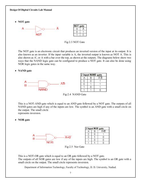
NOT gate<br />
Fig:2.3 NOT Gate<br />
The NOT gate is an electronic circuit that produces an inverted version of the input at its output. It is<br />
also known as an inverter. If the input variable is A, the inverted output is known as NOT A. This is<br />
also shown as A', or A with a bar over the top, as shown at the outputs. The diagrams below show two<br />
ways that the NAND logic gate can be configured to produce a NOT gate. It can also be done using<br />
NOR logic gates in the same way.<br />
NAND gate<br />
Fig:2.4 NAND Gate<br />
This is a NOT-AND gate which is equal to an AND gate followed by a NOT gate. The outputs of all<br />
NAND gates are high if any of the inputs are low. The symbol is an AND gate with a small circle on<br />
the output. The small circle<br />
represents inversion.<br />
NOR gate<br />
Fig:2.5 Nor Gate<br />
This is a NOT-OR gate which is equal to an OR gate followed by a NOT gate.<br />
The outputs of all NOR gates are low if any of the inputs are high. The symbol is an OR gate with a<br />
small circle on the output. The small circle represents inversion.<br />
Department of Information Technology, Faculty of Technology, D. D. <strong>University</strong>, Nadiad.<br />
7