Design Of Digital Circuits - Dharmsinh Desai University
Design Of Digital Circuits - Dharmsinh Desai University
Design Of Digital Circuits - Dharmsinh Desai University

You also want an ePaper? Increase the reach of your titles
YUMPU automatically turns print PDFs into web optimized ePapers that Google loves.
<strong>Design</strong> <strong>Of</strong> <strong>Digital</strong> <strong>Circuits</strong> Lab Manual<br />
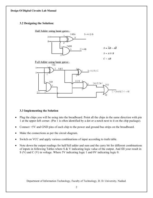
3.2 <strong>Design</strong>ing the Solution:<br />
3.3 Implementing the Solution<br />
<br />
<br />
<br />
<br />
<br />
Plug the chips you will be using into the breadboard. Point all the chips in the same direction with pin<br />
1 at the upper-left corner. (Pin 1 is often identified by a dot or a notch next to it on the chip package).<br />
Connect +5V and GND pins of each chip to the power and ground bus strips on the breadboard.<br />
Make the connections as per the circuit diagram.<br />
Switch on VCC and apply various combinations of input according to truth table.<br />
Note down the output readings for half/full adder and sum and the carry bit for different combinations<br />
of inputs in following Tables where S & V indicating logic value of the output. And fill your result in<br />
S (V) and C (V) in voltage. Where 5V indicating logic 1 and 0V indicating logic 0.<br />
Department of Information Technology, Faculty of Technology, D. D. <strong>University</strong>, Nadiad.<br />
2