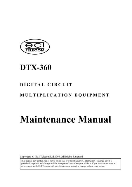
DTX-360 Maintenance Manual - Salvex
DTX-360 Maintenance Manual - Salvex
DTX-360 Maintenance Manual - Salvex

You also want an ePaper? Increase the reach of your titles
YUMPU automatically turns print PDFs into web optimized ePapers that Google loves.
<strong>DTX</strong>-<strong>360</strong><br />
DIGITAL CIRCUIT<br />
MULTIPLICATION EQUIPMENT<br />
<strong>Maintenance</strong> <strong>Manual</strong><br />
Copyright © ECI Telecom Ltd.1998. All Rights Reserved.<br />
This manual may contain minor flaws, omissions, or typesetting errors. Information contained herein is<br />
periodically updated and changes will be incorporated into subsequent editions. If you have encountered an<br />
error, please notify ECI Telecom. All specifications are subject to change without prior notice.
REVISION RECORD<br />
REVISION<br />
01 Preliminary<br />
January 1994<br />
02 First edition and printing<br />
June 1997<br />
03<br />
December 1997<br />
DESCRIPTION<br />
Addition of pages 1-8 to1-11 - Card replacement and card<br />
malfunction detection<br />
04<br />
March 1998 Changes and additions to pages: 5-6, 5-25, 5-35, 1-11-1-14<br />
Publ n No.<br />
92050003
CE MARK COMPLIANCE<br />
The <strong>DTX</strong>-<strong>360</strong> is marked with a CE Mark (see below). This mark has been affixed to<br />
demonstrate full product compliance with the following European directives:<br />
a) Directive 73/23/EEC - Council Directive of 19/02/1973 on the harmonization of the laws<br />
of Member States relating to electrical equipment designed for use within certain voltage<br />
limits.<br />
b) Directive 89/336/EEC - Council Directive of 3/05/1989 on the approximation of laws of<br />
the Member States relating to Electro-Magnetic Compatibility (EMC).<br />
Issue date: 6 February 1996<br />
This document contains proprietary information. It may not, in whole or in part, be published, used, or<br />
reproduced, nor may be disclosed to third parties without the express written permission of ECI Telecom.<br />
© Copyright by ECI Telecom Ltd., 1997<br />
All rights reserved worldwide<br />
ECI Telecom reserves the right, without notice, to make changes in equipment design or<br />
specifications.<br />
Information supplied by ECI Telecom is believed to be accurate and reliable. However, no<br />
responsibility is assumed by ECI Telecom for its use nor for rights of third parties which may<br />
result from its use.<br />
Any representations in this document concerning performance are for informational purposes only<br />
and are not warranties of future performance, either express or implied. ECI Telecom’s standard<br />
limited warranty, stated in its sales contract or order confirmation form, is the only warranty<br />
offered by ECI Telecom.
<strong>DTX</strong>-<strong>360</strong><br />
<strong>Maintenance</strong> <strong>Manual</strong><br />
Table of Contents<br />
Section Description Page<br />
1 GENERAL INFORMATION ..........................................................................1-1<br />
1.1 INTRODUCTION............................................................................................... 1-1<br />
1.2 STATIC AWARENESS ..................................................................................... 1-1<br />
1.3 REPAIR AND RETURN .................................................................................... 1-2<br />
1.3.1 Order Entry (normal shipping time).................................................................... 1-2<br />
1.3.2 Terminal Malfunction Report ............................................................................. 1-2<br />
1.3.3 Order Entry (Emergency Order) ......................................................................... 1-4<br />
1.3.4 Insurance Policy.................................................................................................. 1-4<br />
1.3.5 Substitutions and Modifications ......................................................................... 1-4<br />
1.3.6 Limitations of Liability ....................................................................................... 1-4<br />
1.4 OPS REPAIR ...................................................................................................... 1-5<br />
1.5 TASKS AUTHORIZED FOR THE USER......................................................... 1-5<br />
1.6 HANDLING OF ELECTROSTATICALLY SENSITIVE COMPONENTS ..... 1-5<br />
1.7 HANDLING PRINTED CIRCUIT BOARDS .................................................... 1-6<br />
1.8 HANDLING PERIPHERAL EQUIPMENT AND TERMINALS ..................... 1-6<br />
1.9 HANDLING THE OPERATOR STATION....................................................... 1-7<br />
1.10 AC POWER OUTLETS ..................................................................................... 1-7<br />
1.11 DETECTING CARD MALFUNCTIONS .......................................................... 1-8<br />
1.12 DETECTING THE SOURCE OF A CARD MALFUNCTION......................... 1-8<br />
1.13 CARD REMOVAL UNDER POWER ............................................................. 1-10<br />
1.14 OMCP/COCP CARD REPLACEMENT.......................................................... 1-11<br />
1.14.1 Modifying the ethers file................................................................................... 1-11<br />
1.14.2 Modifying the hosts file .................................................................................... 1-12<br />
1.14.3 Modifying the config file .................................................................................. 1-12<br />
1.14.4 Modifying the pofInfo_am file.......................................................................... 1-12<br />
1.14.5 Resuming Operation.......................................................................................... 1-12<br />
1.15 TO TURN A TERMINAL OFF........................................................................ 1-13<br />
1.15.1 Stand Alone Configuration ............................................................................... 1-13<br />
1.15.2 Cluster configuration......................................................................................... 1-13<br />
2 INTERNAL AND CLUSTER CABLE CONNECTIONS.............................2-1<br />
2.1 GENERAL .......................................................................................................... 2-1<br />
2.2 TERMINAL - LCOM CONNECTIONS ............................................................ 2-2<br />
2.2.1 Bitstream Connection.......................................................................................... 2-2<br />
2.3 LCOM - CCOM CONNECTIONS (FIGURES 2-2 AND 2-3)........................... 2-4<br />
2.3.1 DLC Connections................................................................................................ 2-4<br />
2.3.2 BitstreamConnections ......................................................................................... 2-4<br />
2.4 CCOM - REDUNDANT TERMINAL CONNECTIONS (FIGURES 2-4, 2-5). 2-7<br />
2.4.1 Bitstream Connections ........................................................................................ 2-7<br />
2.4.2 DLC Connections................................................................................................ 2-7<br />
2.4.3 LCOM - Four (4) Compact Terminals Connections (<strong>DTX</strong>-<strong>360</strong>C ) ................. 2-10<br />
2.4.3.1 Bitstream Connections ...................................................................................... 2-10<br />
2.4.3.2 DLC Connections.............................................................................................. 2-10<br />
92050003-03 i
Table of Contents<br />
Section Description Page<br />
2.4.4 SCOM - Three (3) Compact Terminals + Redundant Terminal<br />
Connections (<strong>DTX</strong>-<strong>360</strong>C)................................................................................. 2-12<br />
2.4.4.1 Bitstream Connections ...................................................................................... 2-12<br />
2.4.4.2 DLC Connections.............................................................................................. 2-12<br />
2.4.5 SCOM + Two (2) Terminals + Redundant Terminal Connections................... 2-14<br />
2.4.5.1 Bitstream Connections ...................................................................................... 2-14<br />
2.4.5.2 DLC Connections.............................................................................................. 2-14<br />
3 TRANSMISSION ALARMS............................................................................3-1<br />
3.1 2.048 MBIT/S E1 TRANSMISSION ALARMS DESCRIPTION ..................... 3-1<br />
3.1.1 Loss of Incoming Signal (LOS) .......................................................................... 3-1<br />
3.1.2 Alarm Indication Signal (AIS) ............................................................................ 3-1<br />
3.1.3 Loss of Alignment (LOF) Alarm ........................................................................ 3-2<br />
3.1.4 CRC Multiframe (CRC MFR) ............................................................................ 3-2<br />
3.1.5 High CRC Error .................................................................................................. 3-2<br />
3.1.6 High Bit Error Rate (H.BER).............................................................................. 3-3<br />
3.1.6.1 H.BER, Bitstream with the CRC Format ............................................................ 3-3<br />
3.1.6.2 H.BER, Bitstream without CRC Format............................................................. 3-3<br />
3.1.7 Low Bit Error Rate (L.BER)............................................................................... 3-3<br />
3.1.7.1 L.BER, Bitstream without CRC Format ............................................................. 3-3<br />
3.1.7.2 L.BER, Bitstream with the CRC Format ............................................................ 3-3<br />
3.1.8 Remote (Far-end) Alarm Indication (RAI) ......................................................... 3-3<br />
3.1.9 Multiframe Alignment (MFR) ............................................................................ 3-4<br />
3.1.10 Remote Multiframe Alarm Indication (RMFR).................................................. 3-4<br />
3.1.11 High Slip Rate (H.SLIP) ..................................................................................... 3-4<br />
3.1.12 Low Slip Rate (L.SLIP) ...................................................................................... 3-4<br />
3.1.13 No External Clock Alarm.................................................................................... 3-4<br />
3.1.14 Bitstream or External Clock Fail ........................................................................ 3-5<br />
3.1.15 DCME Frame Alarm (DFA) ............................................................................... 3-5<br />
3.1.16 CC-HBER............................................................................................................ 3-5<br />
3.1.16.1 Activation Criteria............................................................................................... 3-5<br />
3.1.16.2 Deactivation Criteria........................................................................................... 3-5<br />
3.1.17 CC-LBER............................................................................................................ 3-5<br />
3.1.17.1 Activation Criteria............................................................................................... 3-5<br />
3.1.17.2 Deactivation Criteria........................................................................................... 3-6<br />
3.1.18 CC-AIS................................................................................................................ 3-6<br />
3.1.19 Bearer Backward Alarm...................................................................................... 3-6<br />
3.1.20 Far-End (Remote) Trunk Alarm.......................................................................... 3-6<br />
3.2 1.544 MBIT/S T1 TRANSMISSION ALARMS DESCRIPTION ..................... 3-7<br />
3.2.1 Loss Of Frame alignment (LOF - CFA)............................................................ 3-7<br />
3.2.2 Loss Of incoming Signal (LOS) ........................................................................ 3-7<br />
3.2.3 Alarm Indication Signal (AIS-CFA) ................................................................... 3-7<br />
3.2.4 High Bit Error Rate (HBER).............................................................................. 3-8<br />
3.2.5 Remote (Far-end, Distant) Alarm Indication (RAI) - (Yellow)............................ 3-8<br />
3.2.6 Low Bit Error Rate (LBER).............................................................................. 3-9<br />
3.3 MAINTENANCE LEVELS OF TRANSMISSION ALARMS AND<br />
EVENTS (E1 SYSTEM) .................................................................................. 3-10<br />
ii 92050003-02
Table of Contents<br />
Section Description Page<br />
3.4 <strong>Maintenance</strong> Levels of Transmission<br />
Alarms (T1 System) .......................................................................................... 3-13<br />
3.4.1 Change Clock Alarm Severity........................................................................... 3-13<br />
3.5 TRANSMISSION ALARM HANDLING ........................................................ 3-14<br />
4 SYSTEM ALARMS AND EVENTS................................................................4-1<br />
4.1 SYSTEM EVENTS............................................................................................. 4-1<br />
4.2 CCOM EVENTS................................................................................................. 4-3<br />
4.3 OPS ACTIONS ................................................................................................... 4-4<br />
4.4 <strong>DTX</strong>-<strong>360</strong> RESPONSES TO OPS ACTIONS ..................................................... 4-6<br />
4.5 ONLINE BIT TESTS.......................................................................................... 4-9<br />
4.5.1 SIGN Hardware Online Test Options ................................................................. 4-9<br />
4.5.1.1 MFR Trunk (0:15)............................................................................................... 4-9<br />
4.5.1.2 TRUNK OUT Path Test...................................................................................... 4-9<br />
4.5.1.3 CLEAR CHANNEL TRANSMITTER (transparent signaling)......................... 4-9<br />
4.5.1.4 CLEAR CHANNEL RECEIVER ....................................................................... 4-9<br />
4.5.1.5 TRUNK IN Path Test.......................................................................................... 4-9<br />
4.5.1.6 SIGN Loop Back Test......................................................................................... 4-9<br />
4.5.2 AUXC ONLINE BIT ........................................................................................ 4-10<br />
4.5.2.1 DSP TEST......................................................................................................... 4-10<br />
4.5.2.2 PPI TEST .......................................................................................................... 4-10<br />
4.5.2.3 PEB TX TEST .................................................................................................. 4-10<br />
4.5.2.4 PEB RX TEST .................................................................................................. 4-10<br />
4.5.2.5 AUXC 188EC ONLINE EPROM CHECK SUM............................................. 4-10<br />
4.5.2.6 AUXC 188EC ONLINE FLASH CHECK SUM.............................................. 4-10<br />
4.5.2.7 AUXC 188EC ONLINE RAM CHECK........................................................... 4-10<br />
4.5.2.8 AUXC ONLINE INTERRUPT TEST .............................................................. 4-10<br />
4.5.2.9 AUXC 188EC ONLINE TIMER TEST............................................................ 4-10<br />
4.5.3 AUXC 188EC ONLINE HDLC TEST ............................................................. 4-11<br />
4.5.3.1 AUXC 188EC ONLINE DMA TEST............................................................... 4-11<br />
4.5.3.2 AUXC 188C ONLINE PORT TEST ................................................................ 4-11<br />
4.5.4 SCPU 188EC ONLINE BIT.............................................................................. 4-12<br />
4.5.4.1 SCPU ONLINE EPROM CHECK SUM .......................................................... 4-12<br />
4.5.4.2 SCPU ONLINE FLASH CHECK SUM ........................................................... 4-12<br />
4.5.4.3 SCPU ONLINE RAM CHECK ........................................................................ 4-12<br />
4.5.4.4 SCPU ONLINE INTERRUPT TEST................................................................ 4-12<br />
4.5.4.5 SCPU ONLINE TIMER TEST ......................................................................... 4-12<br />
4.5.4.6 SCPU ONLINE HDLC TEST........................................................................... 4-12<br />
4.5.4.7 SCPU ONLINE DMA TEST ............................................................................ 4-12<br />
4.5.4.8 SCPU ONLINE PORT TEST ........................................................................... 4-12<br />
4.5.5 BMCT ONLINE BIT ........................................................................................ 4-13<br />
4.5.5.1 GENERAL ........................................................................................................ 4-13<br />
4.5.5.2 TEST CIRCUIT ................................................................................................ 4-13<br />
4.5.5.3 CONTROL MEMORIES WRITE READ: ....................................................... 4-13<br />
4.5.5.4 BRT BMCT TS0:.............................................................................................. 4-13<br />
4.5.5.5 BMRT BMCT BARKER:................................................................................. 4-13<br />
4.5.5.6 FAX OUT & VBR CONTROL MEMORY: .................................................... 4-13<br />
92050003-02 iii
Table of Contents<br />
Section Description Page<br />
4.5.5.7 BCMODT#N TS0 ............................................................................................. 4-13<br />
4.5.5.8 BMCT ONLINE EPROM CHECK SUM......................................................... 4-13<br />
4.5.5.9 BMCT ONLINE RAM CHECK ....................................................................... 4-13<br />
4.5.5.10 BMCT ONLINE FLASH CHECK SUM.......................................................... 4-13<br />
4.5.5.11 BMCT ONLINE INTERRUPT TEST .............................................................. 4-14<br />
4.5.5.12 BMCT ONLINE TIMER TEST........................................................................ 4-14<br />
4.5.5.13 BMCT ONLINE HDLC TEST ......................................................................... 4-14<br />
4.5.5.14 BMCT ONLINE DMA TEST........................................................................... 4-14<br />
4.5.5.15 BMCT ONLINE PORT TEST.......................................................................... 4-14<br />
4.5.6 BMCR CPU ONLINE TEST ............................................................................ 4-15<br />
4.5.6.1 GENERAL ........................................................................................................ 4-15<br />
4.5.6.2 CONTROL MEMORIES WRITE READ ........................................................ 4-15<br />
4.5.6.3 BCBSR#N TS0 ................................................................................................. 4-15<br />
4.5.6.4 BCMDR#N TS0................................................................................................ 4-15<br />
4.5.6.5 FAXBSR#N TS0............................................................................................... 4-15<br />
4.5.6.6 BMCR ONLINE EPROM CHECK SUM......................................................... 4-15<br />
4.5.6.7 BMCR ONLINE RAM CHECK....................................................................... 4-15<br />
4.5.6.8 BMCR ONLINE FLASH CHECK SUM.......................................................... 4-15<br />
4.5.6.9 BMCR ONLINE INTERRUPT TEST.............................................................. 4-15<br />
4.5.6.10 BMCR ONLINE TIMER TEST ....................................................................... 4-16<br />
4.5.6.11 BMCR ONLINE HDLC TEST ......................................................................... 4-16<br />
4.5.6.12 BMCR ONLINE DMA TEST........................................................................... 4-16<br />
4.5.6.13 BMCR ONLINE PORT TEST.......................................................................... 4-16<br />
4.5.7 CKSL ONLINE BIT SPECIFICATIONS......................................................... 4-17<br />
4.5.7.1 PPI DATA BUS TEST...................................................................................... 4-17<br />
4.5.7.2 CKSL 12V TEST.............................................................................................. 4-17<br />
4.5.7.3 PLL LOCK TEST ............................................................................................. 4-17<br />
4.5.7.4 TIMING TEST.................................................................................................. 4-17<br />
4.5.8 XDSP ONLINE BIT (SDSP/TDSP/RDSP) ...................................................... 4-18<br />
4.5.8.1 GENERAL ........................................................................................................ 4-18<br />
4.5.8.2 SDSP ODD CELL TEST .................................................................................. 4-18<br />
4.5.8.3 XDSP HDLC PORT ......................................................................................... 4-18<br />
4.5.8.4 XDSP DSP_RES1 PORT.................................................................................. 4-18<br />
4.5.8.5 XDSP DSP_RES2 PORT.................................................................................. 4-18<br />
4.5.8.6 XDSP BS CM DATA TEST............................................................................. 4-18<br />
4.5.8.7 XDSP DSP CELL 0-15 TEST .......................................................................... 4-18<br />
4.5.8.8 188EC ONLINE EPROM CHECK SUM......................................................... 4-18<br />
4.5.8.9 188EC ONLINE FLASH CHECK SUM .......................................................... 4-18<br />
4.5.8.10 188EC ONLINE RAM CHECK ....................................................................... 4-19<br />
4.5.8.11 188EC ONLINE INTERRUPT TEST .............................................................. 4-19<br />
4.5.8.12 188EC ONLINE TIMER TEST........................................................................ 4-19<br />
4.5.8.13 188EC ONLINE HDLC TEST ......................................................................... 4-19<br />
4.5.8.14 188EC ONLINE DMA TEST........................................................................... 4-19<br />
4.5.8.15 188C ONLINE PORT TEST............................................................................. 4-19<br />
4.5.8.16 TDSP CELL TEST ........................................................................................... 4-19<br />
4.5.8.17 FDSP CELL TEST............................................................................................ 4-19<br />
4.5.8.18 RDSP ODD CELLS TEST ............................................................................... 4-20<br />
iv 92050003-02
Table of Contents<br />
Section Description Page<br />
4.5.9 XCPU ONLINE TEST...................................................................................... 4-21<br />
4.5.9.1 XCPU ONLINE EPROM CHECK SUM ......................................................... 4-21<br />
4.5.9.2 XCPU ONLINE RAM CHECK........................................................................ 4-21<br />
4.5.9.3 XCPU ONLINE FLASH CHECK SUM........................................................... 4-21<br />
4.5.9.4 XCPU ONLINE INTERRUPT TEST............................................................... 4-21<br />
4.5.9.5 XCPU ONLINE TIMER TEST ........................................................................ 4-21<br />
4.5.9.6 XCPU ONLINE HDLC TEST.......................................................................... 4-21<br />
4.5.9.7 XCPU ONLINE DMA TEST ........................................................................... 4-21<br />
4.5.9.8 XCPU ONLINE PORT TEST........................................................................... 4-21<br />
4.5.10 OMCP ONLINE TEST ..................................................................................... 4-22<br />
4.5.10.1 OMCP ONLINE EPROM CHECK SUM......................................................... 4-22<br />
4.5.10.2 OMCP ONLINE RAM CHECK ....................................................................... 4-22<br />
4.5.10.3 OMCP ONLINE FLASH CHECK SUM.......................................................... 4-22<br />
4.5.10.4 OMCP ONLINE INTERRUPT TEST .............................................................. 4-22<br />
4.5.10.5 OMCP ONLINE TIMER TEST........................................................................ 4-22<br />
4.5.10.6 OMCP ONLINE HDLC TEST ......................................................................... 4-22<br />
4.5.10.7 OMCP ONLINE DMA TEST........................................................................... 4-22<br />
4.5.10.8 OMCP ONLINE LAN CONTROLLER TEST................................................. 4-22<br />
4.5.10.9 OMCP ONLINE REAL TIME CLOCK TEST ................................................ 4-22<br />
4.5.10.10 OMCP ONLINE POWER FAILURE TEST .................................................... 4-23<br />
4.5.10.11 OMCP ONLINE PORT TEST.......................................................................... 4-23<br />
4.5.11 DSIT TEST DESCRIPTION............................................................................. 4-24<br />
4.5.11.1 GENERAL ........................................................................................................ 4-24<br />
4.5.11.2 DSIT T_PPI TEST ............................................................................................ 4-24<br />
4.5.11.3 DSIT XILINX TEST......................................................................................... 4-24<br />
4.5.11.4 DSIT 12 TEST .................................................................................................. 4-24<br />
4.5.11.5 DSIT PLL TEST ............................................................................................... 4-24<br />
4.5.11.6 ACFA TEST (Alarm Simulation) ..................................................................... 4-24<br />
4.5.11.7 TS0 PATTERN GENERATOR TEST ............................................................. 4-24<br />
4.5.11.8 DSIT INPUT BITSTREAMS TEST................................................................. 4-24<br />
4.5.11.9 DSIT ENC2BC MATRIX TEST ...................................................................... 4-24<br />
4.5.12 DSIT ENC2BC MATRIX INPUT BITSTREAMS BIT................................... 4-25<br />
4.5.12.1 DSIT MODE MATRIX TEST.......................................................................... 4-25<br />
4.5.12.2 DSIT MODE MATRIX INPUT BS TEST (TS0 TEST) .................................. 4-25<br />
4.5.12.3 DSIT DMUX CM TEST................................................................................... 4-25<br />
4.5.12.4 DSIT TDSI1 MATRIX TEST........................................................................... 4-25<br />
4.5.12.5 DSIT TDSI2 MATRIX TEST........................................................................... 4-25<br />
4.5.12.6 DSIT SHORT DELAY MEMORY TEST........................................................ 4-25<br />
4.5.12.7 DSIT LONG DELAY MEMORY TEST.......................................................... 4-25<br />
4.5.12.8 DSIT SIGNAL GENERATOR TEST............................................................... 4-25<br />
4.5.12.9 DSIT FPD (FAX PATTERN DETECTOR) TEST .......................................... 4-25<br />
4.5.12.10 DSIT SMAT TS0 TEST ................................................................................... 4-25<br />
4.5.13 ADPC ONLINE GENERIC DESCRIPTION ................................................... 4-26<br />
4.5.13.1 DPR Test ........................................................................................................... 4-26<br />
4.5.13.2 Output Ports Test .............................................................................................. 4-26<br />
4.5.13.3 PLL Lock Test................................................................................................... 4-26<br />
4.5.13.4 Test For The Codecs BIT Machine................................................................... 4-26<br />
92050003-02 v
Table of Contents<br />
Section Description Page<br />
4.5.13.5 Codecs Built-in Test.......................................................................................... 4-26<br />
4.5.13.6 ADPC Bitstream Test (TS0 Test) ..................................................................... 4-27<br />
4.5.14 QDLI ONLINE BIT DESCRIPTION ............................................................... 4-28<br />
4.5.14.1 GENERAL ........................................................................................................ 4-28<br />
4.5.14.2 PPI TEST .......................................................................................................... 4-28<br />
4.5.14.3 QDLI ACFA DATA BUS TEST ...................................................................... 4-28<br />
4.5.14.4 QDLI Xilinx REGISTERS TEST ..................................................................... 4-28<br />
4.5.14.5 QDLI LIU OSL TEST....................................................................................... 4-28<br />
4.5.14.6 QDLI ACFA PARITY CHECK........................................................................ 4-28<br />
4.5.14.7 QDLI LOCAL TS0 PATTERN GENERATOR TEST..................................... 4-28<br />
4.5.14.8 QDLI OUTPUT BITSTREAM TESTS ............................................................ 4-28<br />
4.5.14.9 QDLI INPUT BITSTREAM TEST .................................................................. 4-28<br />
4.5.14.10 QDLI LOOP BACK TEST ............................................................................... 4-28<br />
4.5.15 RDSW TEST..................................................................................................... 4-30<br />
4.5.16 TSDF ONLINE BIT DESCRIPTION ............................................................... 4-31<br />
4.5.16.1 GENERAL ........................................................................................................ 4-31<br />
4.5.16.2 TSDF PPI TEST................................................................................................ 4-31<br />
4.5.16.3 TSDF ACFA TEST (ALARM SIMULATION)............................................... 4-31<br />
4.5.16.4 TSDF LOCAL TS0 GENERATOR TEST ....................................................... 4-31<br />
4.5.16.5 TSDF MATRIX TEST DESCRIPTION........................................................... 4-32<br />
4.5.16.6 TSDF MATRIX SYNC TEST.......................................................................... 4-32<br />
4.5.16.7 TSDF MATRIX CM TEST .............................................................................. 4-32<br />
4.5.16.8 TSDF MATRIX SWITCH TEST ..................................................................... 4-32<br />
4.5.16.9 TSDF MATRIX INPUT BS TEST ................................................................... 4-32<br />
4.5.16.10 TSDF MATRIX DEVICES .............................................................................. 4-32<br />
4.5.17 DSIR ONLINE BIT DESCRIPTION................................................................ 4-33<br />
4.5.17.1 GENERAL ........................................................................................................ 4-33<br />
4.5.17.2 DSIR R_PPI TEST............................................................................................ 4-33<br />
4.5.17.3 DSIR XILINX TEST ........................................................................................ 4-33<br />
4.5.17.4 DSIR 12 TEST .................................................................................................. 4-33<br />
4.5.17.5 DSIR PLL TEST ............................................................................................... 4-33<br />
4.5.17.6 ACFA TEST (Alarm Simulation) ..................................................................... 4-33<br />
4.5.17.7 TS0 PATTERN GENERATOR TEST ............................................................. 4-33<br />
4.5.17.8 DSIR INPUT BITSTREAMS TEST................................................................. 4-33<br />
4.5.17.9 DSIR RDSI MATRIX TEST ............................................................................ 4-33<br />
4.5.17.10 DSIR MDSW MATRIX TEST......................................................................... 4-33<br />
4.5.17.11 DSIR MDSW MATRIX TEST INPUT BITSTREAMS TEST........................ 4-34<br />
4.5.17.12 DSIR INLV MATRIX TEST............................................................................ 4-34<br />
4.5.17.13 DSIR INLV MATRIX INPUT BS TEST (TS0 TEST) .................................... 4-34<br />
4.5.17.14 DSIR RDSP INPUT BS TEST (RDSP EVEN CELL TEST)........................... 4-34<br />
4.5.17.15 DSIR ADPC-RX INPUT BITSTREAMS TEST .............................................. 4-34<br />
4.5.17.16 DSIR TSDF INPUT BITSTREAMS TEST...................................................... 4-34<br />
4.5.17.17 DSIR “TEST-DSP” TEST ................................................................................ 4-34<br />
4.6 BUILT-IN TEST DIAGNOSTICS.................................................................... 4-35<br />
vi 92050003-02
Table of Contents<br />
Section Description Page<br />
5 JUMPER SETTINGS .......................................................................................5-1<br />
5.1 <strong>DTX</strong> - <strong>360</strong> TERMINAL, CARD LAYOUT ....................................................... 5-1<br />
5.2 <strong>DTX</strong> - <strong>360</strong>C COMPACT TERMINAL, CARD LAYOUT ................................ 5-1<br />
5.3 <strong>DTX</strong> - <strong>360</strong> TERMINAL, LIST OF CARD JUMPER SETTINGS..................... 5-2<br />
5.4 AUXC ................................................................................................................. 5-3<br />
5.4.1 AUXC Jumper Settings....................................................................................... 5-3<br />
5.4.2 AUXC Hard Wired ............................................................................................. 5-3<br />
5.4.3 AUXC Location of Jumpers ............................................................................... 5-3<br />
5.5 ADPC & ADPX .................................................................................................. 5-4<br />
5.5.1 ADPC & ADPX Jumper Settings - None............................................................ 5-4<br />
5.5.2 ADPC & ADPX Hard Wired .............................................................................. 5-4<br />
5.5.3 ADPC & ADPX Location of Jumpers ................................................................ 5-4<br />
5.6 CPU..................................................................................................................... 5-5<br />
5.6.1 CPU Jumper Settings .......................................................................................... 5-5<br />
5.6.2 CPU Hard Wired................................................................................................. 5-5<br />
5.6.3 CPU DIP Switch (U72) Settings ......................................................................... 5-5<br />
5.6.4 CPU Location of Jumpers and DIP Switches ..................................................... 5-5<br />
5.7 OMCP ................................................................................................................. 5-6<br />
5.7.1 OMCP Jumper Settings....................................................................................... 5-6<br />
5.7.2 OMCP Hard Wired ............................................................................................. 5-6<br />
5.7.3 OMCP DIP Switch (U51) Settings ..................................................................... 5-6<br />
5.7.4 OMCP Location of Jumpers and DIP Switches.................................................. 5-6<br />
5.8 BPIF/1 ................................................................................................................. 5-7<br />
5.8.1 BPIF /1 Jumper Settings...................................................................................... 5-7<br />
5.8.2 BPIF /1 Hard Wired - None ................................................................................ 5-7<br />
5.8.3 BPIF /1 Location of Jumpers and DIP Switches................................................. 5-7<br />
5.8.4 BMCT ................................................................................................................. 5-7<br />
5.8.5 BMCT Jumper Settings....................................................................................... 5-7<br />
5.8.6 BMCT Hard Wired - None ................................................................................. 5-8<br />
5.8.7 BMCT DIP Switch SW1 Settings....................................................................... 5-8<br />
5.8.8 BMCT Location of Jumpers and DIP Switches.................................................. 5-8<br />
5.8.9 DSP ..................................................................................................................... 5-8<br />
5.8.10 DSP Jumper Settings........................................................................................... 5-8<br />
5.8.11 DSP Hard Wired - None ..................................................................................... 5-8<br />
5.8.12 DSP DIP Switch (U102) Settings ....................................................................... 5-9<br />
5.8.13 DSP Location of Jumpers and DIP Switches...................................................... 5-9<br />
5.9 RDSW ............................................................................................................... 5-10<br />
5.9.1 RDSW Jumper Settings..................................................................................... 5-10<br />
5.9.2 RDSW Hard Wired - None ............................................................................... 5-10<br />
5.9.3 RDSW Location of Jumpers and DIP Switches................................................ 5-10<br />
5.10 QDLI ................................................................................................................. 5-11<br />
5.10.1 QDLI Jumper Settings....................................................................................... 5-11<br />
5.10.2 QDLI Hard Wired - None ................................................................................. 5-12<br />
5.10.3 QDLI DIP Switch (U43) Settings ..................................................................... 5-12<br />
5.10.4 QDLI Location of Jumpers and DIP Switches.................................................. 5-12<br />
5.10.5 QDLI Rev. E Jumper Settings........................................................................... 5-13<br />
92050003-02 vii
Table of Contents<br />
Section Description Page<br />
5.10.6 QDLI REV. E Hard Wired................................................................................ 5-14<br />
5.10.7 QDLI REV.-E DIP Switch (U75) Settings........................................................ 5-14<br />
5.10.8 QDLI REV.-E Location of Jumpers and DIP Switches .................................... 5-14<br />
5.11 CKSL................................................................................................................. 5-15<br />
5.11.1 CKSL Jumper Settings...................................................................................... 5-15<br />
5.11.2 CKSL Hard Wired ............................................................................................ 5-15<br />
5.11.3 CKSL Location of Jumpers............................................................................... 5-15<br />
5.12 BPIF/0 ............................................................................................................... 5-16<br />
5.12.1 BPIF /0 Jumper Settings.................................................................................... 5-16<br />
5.12.2 BPIF /0 Hard Wired - None .............................................................................. 5-16<br />
5.12.3 BPIF /0 Location of Jumpers ............................................................................ 5-16<br />
5.13 SIGN & SIGN/L *............................................................................................. 5-17<br />
5.13.1 SIGN Jumper Settings....................................................................................... 5-17<br />
5.13.2 SIGN Hard Wired - None.................................................................................. 5-17<br />
5.13.3 SIGN Location of Jumpers................................................................................ 5-17<br />
5.14 TSDF................................................................................................................. 5-18<br />
5.14.1 TSDF Jumper Settings - None .......................................................................... 5-18<br />
5.14.2 TSDF Hard Wired............................................................................................. 5-18<br />
5.14.3 TSDF Location of Jumpers............................................................................... 5-18<br />
5.15 BPIF/2 ............................................................................................................... 5-19<br />
5.15.1 BPIF /2 Jumper Settings.................................................................................... 5-19<br />
5.15.2 BPIF /2 Hard Wired - None .............................................................................. 5-19<br />
5.15.3 BPIF /2 Location of Jumpers ............................................................................ 5-19<br />
5.16 BMCR ............................................................................................................... 5-20<br />
5.16.1 BMCR Jumper Settings..................................................................................... 5-20<br />
5.16.2 BMCR Hard Wired - None ............................................................................... 5-20<br />
5.16.3 BMCR DIP Switch (SW1) Settings .................................................................. 5-20<br />
5.16.4 BMCR Location of Jumpers and DIP Switches................................................ 5-20<br />
5.17 BPIF/3 ............................................................................................................... 5-21<br />
5.17.1 BPIF /3 Jumper Settings.................................................................................... 5-21<br />
5.17.2 BPIF /3 Hard Wired - None .............................................................................. 5-21<br />
5.17.3 BPIF /3 Location of Jumpers and DIP Switches............................................... 5-21<br />
5.18 GDSP................................................................................................................. 5-22<br />
5.18.1 GDSP Jumper Settings...................................................................................... 5-22<br />
5.18.2 GDSP Hard Wired - None................................................................................ 5-22<br />
5.18.3 GDSP DIP Switch (U102) Settings................................................................... 5-22<br />
5.18.4 GDSP Location of Jumpers and DIP Switches................................................. 5-22<br />
5.19 DSIR /L ............................................................................................................. 5-23<br />
5.19.1 DSIR /L Jumper Settings .................................................................................. 5-23<br />
5.19.2 DSIR /L Hard Wired - None ............................................................................. 5-23<br />
5.19.3 DSIR /L Location of Jumpers ........................................................................... 5-23<br />
5.20 CPU /L .............................................................................................................. 5-24<br />
5.20.1 CPU /L Jumper Settings.................................................................................... 5-24<br />
5.20.2 CPU /L DIP Switch (U61) Settings .................................................................. 5-24<br />
5.20.3 CPU /L Location of Jumpers and DIP Switches............................................... 5-24<br />
5.21 OMCP /L........................................................................................................... 5-25<br />
5.21.1 OMCP /L Jumper Settings ................................................................................ 5-25<br />
viii 92050003-02
Table of Contents<br />
Section Description Page<br />
5.21.2 OMCP /L Hard Wired....................................................................................... 5-25<br />
5.21.3 OMCP /L DIP Switch (S2) Settings.................................................................. 5-25<br />
5.21.4 OMCP /L Location of Jumpers and DIP Switches ........................................... 5-25<br />
5.22 BMCT /L........................................................................................................... 5-26<br />
5.22.1 BMCT /L Jumper Settings ................................................................................ 5-26<br />
5.22.2 BMCT /L Hard Wired - None........................................................................... 5-26<br />
5.22.3 BMCT /L DIP Switch (SW2) Settings.............................................................. 5-27<br />
5.22.4 BMCT /L Location of Jumpers and DIP Switches ........................................... 5-27<br />
5.23 TSDF /L ............................................................................................................ 5-28<br />
5.23.1 TSDF /L On Circuit Wired (Hard Wired)......................................................... 5-28<br />
5.23.2 TSDF /L Location of Jumpers .......................................................................... 5-28<br />
5.24 BMCR /L........................................................................................................... 5-29<br />
5.24.1 BMCR /L Jumper Settings................................................................................ 5-29<br />
5.24.2 BMCR /L Hard Wired - None........................................................................... 5-29<br />
5.24.3 BMCR /L DIP Switch (SW2) Settings.............................................................. 5-29<br />
5.24.4 BMCR /L Location of Jumpers and DIP Switches ........................................... 5-29<br />
5.25 DSIT /L ............................................................................................................. 5-30<br />
5.25.1 DSIT /L Jumper Settings................................................................................... 5-30<br />
5.25.2 DSIT /L Hard Wired - None ............................................................................. 5-30<br />
5.25.3 DSIT /L Location of Jumpers ........................................................................... 5-30<br />
5.26 LDCH REV A ................................................................................................... 5-31<br />
5.26.1 LDCH Jumper Settings ..................................................................................... 5-31<br />
5.26.2 LDCH Hard Wired - None............................................................................... 5-31<br />
5.26.3 LDCH DIP Switch (S2) Settings....................................................................... 5-31<br />
5.26.4 LDCH Location of Jumpers............................................................................. 5-31<br />
5.27 LDCH REV B ................................................................................................... 5-32<br />
5.27.1 LDCH Jumper Settings ..................................................................................... 5-32<br />
5.27.2 LDCH Hard Wired - None................................................................................ 5-32<br />
5.27.3 LDCH DIP Switch (S2) Settings- None............................................................ 5-32<br />
5.27.4 LDCH Location of Jumpers.............................................................................. 5-32<br />
5.28 CCOM............................................................................................................... 5-33<br />
5.28.1 CCOM Cards Layout ........................................................................................ 5-33<br />
5.28.2 CCOM List of Card Jumper Settings............................................................... 5-33<br />
5.29 CRIO JUMPER SETTINGS ............................................................................. 5-34<br />
5.29.1 CRIO Hard Wired - None ................................................................................. 5-34<br />
5.29.2 CRIO Location of Jumpers ............................................................................... 5-34<br />
5.30 COCP ................................................................................................................ 5-35<br />
5.30.1 COCP Jumper Settings...................................................................................... 5-35<br />
5.30.2 COCP Hard Wired - None ................................................................................ 5-35<br />
5.30.3 COCP DIP Switch (SW2) Settings ................................................................... 5-35<br />
5.30.4 COCP Location of Jumpers and DIP Switches................................................. 5-35<br />
5.31 LCOM ............................................................................................................... 5-36<br />
5.31.1 LCOM Cards Layout......................................................................................... 5-36<br />
5.31.2 LCOM List of Card Jumper Settings ................................................................ 5-36<br />
5.32 SCOM ............................................................................................................... 5-36<br />
5.32.1 SCOM Cards Layout......................................................................................... 5-36<br />
5.33 LCMB ............................................................................................................... 5-37<br />
92050003-02 ix
Table of Contents<br />
Section Description Page<br />
5.33.1 LCMB Jumper Settings - None......................................................................... 5-37<br />
5.33.2 LCMB Hard Wired - None ............................................................................... 5-37<br />
5.33.3 LCMB DIP Switches (SW2 to SW6) Settings.................................................. 5-37<br />
5.34 LRMX ............................................................................................................... 5-38<br />
5.34.1 LRMX Jumper Settings (for 75Ω or 100Ω) ..................................................... 5-38<br />
5.34.2 LRMX Hard Wired - None ............................................................................... 5-38<br />
5.35 LRMX ............................................................................................................... 5-39<br />
5.35.1 LRMX Jumper Settings - None......................................................................... 5-39<br />
5.35.2 LRMX Hard Wired - for 120Ω ......................................................................... 5-39<br />
5.36 POWER SUPPLY............................................................................................. 5-40<br />
5.36.1 Power Supply Front Panel................................................................................. 5-40<br />
5.36.2 Power Supply Shelf........................................................................................... 5-40<br />
5.37 MBPU ............................................................................................................... 5-41<br />
5.37.1 MBPU Jumper Settings..................................................................................... 5-41<br />
5.37.2 MBPU Hard Wired - None ............................................................................... 5-41<br />
5.37.3 MBPU DIP Switch Settings .............................................................................. 5-41<br />
5.38 SUMMARY OF JUMPER AND SWITCH SETTINGS.................................. 5-42<br />
5.38.1 <strong>DTX</strong>-<strong>360</strong> Cards................................................................................................. 5-42<br />
5.38.2 Trunk & Bearer Impedance Configuration ....................................................... 5-44<br />
5.39 CCOM CARDS................................................................................................. 5-45<br />
5.40 LCOM CARDS................................................................................................. 5-46<br />
5.40.1 Trunk & Bearer Impedance Configuration ....................................................... 5-46<br />
5.41 POWER SUPPLY SHELF CARDS.................................................................. 5-47<br />
x 92050003-02
1<br />
GENERAL INFORMATION<br />
1.1 Introduction<br />
This manual identifies and explains maintenance concepts and features with regard to<br />
the <strong>DTX</strong>-<strong>360</strong> system. It outlines procedures to aid maintenance personnel with<br />
troubleshooting diagnosis, fault isolation, analysis, location, and correction.<br />
1.2 Static Awareness<br />
The <strong>DTX</strong>-<strong>360</strong> is designed for easy maintenance. Prior to maintenance, however, it<br />
should be noted that there are SPECIAL PRECAUTIONS that should be followed. It<br />
must be remembered that electronic devices are easily damaged by accidental<br />
introduction of ground or foreign voltages. Therefore, certain tools and test equipment<br />
commonly used on electro-mechanical systems should never be used on an electronic<br />
system. These include: battery buzzers, AC wire-wrap guns, electric soldering irons,<br />
guns, test picks, and test lamps. The following precautions must be observed:<br />
a. The <strong>DTX</strong>-<strong>360</strong> uses various metal oxide semiconductor (MOS) devices. Special<br />
handling of circuit cards which contain these devices is required. All personal<br />
tools, test equipment, and metal objects that come in contact with MOS devices<br />
must be electrically grounded. Any static or foreign voltage that is introduced<br />
into these devices may damage them permanently.<br />
b. DO NOT use tools or test equipment that draw an appreciable amount of current<br />
when attached to the system, such as test lamps and picks.<br />
c. DO NOT use tools or test equipment that could introduce foreign voltages into<br />
the system. For example, a battery-powered buzzer operates on only six or nine<br />
volts, but the voltage introduced across the buzzer coil when the magnetic field<br />
collapsed, can reach a momentary peak in excess of 100 volts, which can<br />
destroy solid- state devices.<br />
92050003-02 1-1
Section 1<br />
General<br />
<strong>DTX</strong>-<strong>360</strong><br />
<strong>Maintenance</strong><br />
1.3 Repair and Return<br />
Repair and return orders are issued to fix customer-owned material where service<br />
conditions do not require advance replacement or when least- costly service is desired.<br />
Generally, repair and return orders are mailed into the Material Service Center (MSC).<br />
The MSC will repair or replace (with repaired equipment) at our option, materials<br />
returned to our facilities.<br />
Note: If the system ceases to respond and/or operate (freezes), perform a Power Up Reset, verify<br />
return to proper operation and report immediately to ECI Telecom Field Engineering<br />
Department, specifying all relevant information, including History Report etc.<br />
1.3.1 Order Entry (normal shipping time)<br />
Repair of defective materials is handled by calling your MSC representative. You will be issued<br />
an Order Control Number that will serve as your Return Authorization (RA). Each package<br />
returned should be clearly identified with the RA number. A complete description of failure<br />
symptoms should be enclosed for each returned part (Fig. 1-1). Shipment to the MSC must be<br />
complete; do not send parts separately - some at one time and others at a later date. The MSC<br />
representative will prepare an order and file it in our receiving area pending arrival of the parts.<br />
Send the materials when the Return Authorization number is received.<br />
a) Typical Delivery Interval<br />
Thirty days should be allowed for our repair time starting from when your<br />
materials are received by the MSC and when the materials are shipped back.<br />
b) Invoicing Policy<br />
In-warranty repair service is done at no charge. You pay the freight inbound<br />
and we will pay the outbound freight. A "no charge" invoice will be sent to you<br />
to close your purchase order. Premium freight service, if requested, will be<br />
invoiced to the customer. All terms are net 30 days.<br />
Out-of-warranty invoices on repaired parts will generally be at 40% of full list<br />
price plus freight and taxes for equipment manufactured by ECI Telecom.<br />
However, major repairs will require cost estimates prior to completion of work.<br />
In this case, a price quotation will be supplied with the repair order confirmation<br />
prior to the start of repair work. All terms are net 30 days.<br />
1.3.2 Terminal Malfunction Report<br />
In the rare event that a terminal ceases to operate, and is “stuck”, please do the<br />
following:<br />
• Perform a Power Up Reset<br />
• Verify return (of the terminal) to proper operation<br />
• Report to ECI Telecom as soon as possible - Please attach to your report all relevant<br />
information, such as History Reports.<br />
1-2 92050003-04
<strong>DTX</strong>-<strong>360</strong> Section 1<br />
<strong>Maintenance</strong><br />
General<br />
MSC LOCATIONS<br />
ECI Telecom Inc.<br />
927 Fern Street<br />
Altamonte Springs, FL 32701<br />
USA<br />
Tel: +1-407-331-5500<br />
Fax: +1-407-260-7136<br />
ECI Telecom GmbH<br />
Büropark Oberursel<br />
In der Au 27<br />
61440 Oberursel/Taunus<br />
Germany<br />
Tel: +49-6171-6209-0<br />
Fax: +49-6171-6209-88<br />
ECI Telecom (UK) Ltd.<br />
ISIS House, Reading Road<br />
Basingstoke<br />
Hampshire RG24 8TW England<br />
Tel: +44-1256-388000<br />
Fax: +44-1256-388180<br />
ECI Telecom (HK) Ltd.<br />
2806 China Resources Building<br />
26 Harbour Road, Wanchai<br />
Hong Kong<br />
Tel: +852-2824-4128<br />
Fax: +852-2802-4411<br />
Description Serial No. Revision<br />
Descripción No. de serie Revisión<br />
Déscription Numéro de serie Révision<br />
Beschreibung Serial No. Revision<br />
Company Country City<br />
Compania Pais Ciudad<br />
Compagnie Pays Ville<br />
Gesellschaft Land Stadt<br />
System No. Site Date<br />
Sistema No. Ubicación Fecha<br />
Numéro de système Site Date<br />
Anlage Stelle Datum<br />
-------------------------------------------------------<br />
Description of Fault<br />
Descripción de la falla<br />
Déscription de panne<br />
Beschreibung der Fehler<br />
Name<br />
Nombre<br />
Nom<br />
Name<br />
Signature<br />
Firma<br />
Signature<br />
Unterschrift<br />
Figure 1-1. Malfunction Report<br />
92050003-04 1-3
Section 1<br />
General<br />
<strong>DTX</strong>-<strong>360</strong><br />
<strong>Maintenance</strong><br />
1.3.3 Order Entry (Emergency Order)<br />
Enter your emergency service orders by calling the MSC and providing us with your<br />
materials requirements; warranty status, air express shipping instructions, purchase<br />
order number and name of the person authorizing the purchase order.<br />
For service call your local agent.<br />
a) Method of Shipment<br />
High priority orders must be shipped via express/traceable means; regular orders<br />
may be shipped via any standard available carrier as directed by the customer.<br />
Shipment number and other delivery information may be obtained by calling the<br />
MSC. A return authorization and pre-addressed return labels are sent with all inwarranty<br />
shipments to facilitate your immediate return of the defective<br />
equipment.<br />
b) Invoicing Policy/Payment Terms<br />
1.3.4 Insurance Policy<br />
In-warranty shipments are not invoiced immediately to allow you 30 days from<br />
date of shipment to return the defective equipment. Out-of-warranty shipments<br />
are invoiced immediately.<br />
ECI Telecom will insure, at its own expense, materials shipped from ECI to customers.<br />
However, materials shipped from a customer's location to the MSC by the customer<br />
must be insured by the customer at his own expense.<br />
1.3.5 Substitutions and Modifications<br />
ECI reserves the right to make substitutions and modifications in the specifications of<br />
equipment designed by ECI that do not materially and adversely affect the performance<br />
of the equipment.<br />
1.3.6 Limitations of Liability<br />
Except as described under "Warranty", ECI shall not be liable for any liability, loss,<br />
damage, or expense relating to, arising out of, or in connection with the purchase,<br />
operation, use of licensing of equipment, software, and services. In no event shall ECI<br />
be liable for any SPECIAL, indirect, accidental, or consequential damages of any nature,<br />
regardless of whether ECI has been advised of the possibility of such damages.<br />
1-4 92050003-04
<strong>DTX</strong>-<strong>360</strong> Section 1<br />
<strong>Maintenance</strong><br />
General<br />
1.4 OPS Repair<br />
Repair of the "SUN" workstation used in the <strong>DTX</strong>-<strong>360</strong> system as an OPS is provided by<br />
your local "SUN" service office. Repair of defective OPS is handled by calling your<br />
MSC representative who will, in turn, arrange all the necessary procedures with the<br />
SUN service office.<br />
When all the procedures are arranged, your MSC representative will inform you about<br />
his arrangements. He also will inform you whether the repair is an in-warranty or out-ofwarranty<br />
service. After all the procedures have been done, you may send your defective<br />
OPS to the service center, following your MSC representative`s instructions.<br />
During the warranty period the OPS will be repaired at no charge by the local service<br />
office. During the out-of-warranty period you will be charged by the "SUN" service<br />
office for the OPS repair.<br />
1.5 Tasks Authorized for the User<br />
The user may perform the following repair and testing actions:<br />
❑ Connecting/disconnecting plug-in cables in the <strong>DTX</strong>-<strong>360</strong> system.<br />
❑ Extracting and inserting any PCB in the <strong>DTX</strong>-<strong>360</strong> card cage. With the exception of<br />
the line-interface cards, power supply units, and the redundant cards in the changeover<br />
matrix, all other cards should be removed only with the power switched OFF.<br />
Note: Use of a grounding strap is obligatory when a PCB is being extracted or<br />
inserted into the card cage.<br />
❑ Connecting and disconnecting DC-power (or AC) cable(s) (if applicable), to the<br />
<strong>DTX</strong>-<strong>360</strong> system and its peripheral equipment and/or operator station<br />
❑ Performing all test procedures described in this <strong>Manual</strong><br />
1.6 Handling of Electrostatically Sensitive Components<br />
The <strong>DTX</strong>-<strong>360</strong> uses MOS Semiconductor devices. Special handling precautions must be<br />
observed when handling PCBs. All personal tools, test equipment, and metal objects that<br />
come in contact with MOS devices must be electrically grounded. Any static and/or<br />
external voltage that is introduced into these devices can damage them permanently.<br />
Personnel handling PCBs should be grounded, using a grounding strap.<br />
92050003-04 1-5
Section 1<br />
General<br />
<strong>DTX</strong>-<strong>360</strong><br />
<strong>Maintenance</strong><br />
1.7 Handling Printed Circuit Boards<br />
❑ Do not rub, scratch, or scrape the printed wiring side with a sharp or abrasive object.<br />
❑ Do not expose to excessive heat or humidity.<br />
❑ Do not make any unauthorized modifications, repairs, or adjustments.<br />
❑ Do not use abrasive cleaners.<br />
❑ Do not mark the cards with any writing instrument that leaves a conductive deposit,<br />
such as lead pencil.<br />
❑ Do not stack PCBs on top of each other.<br />
❑ Do not store PCBs in an area that contains air pollutants (gas, smoke, dust, etc.) that<br />
may contain harmful agents. Store PCBs in anti-static conductive bags.<br />
1.8 Handling Peripheral Equipment and Terminals<br />
Several external devices may be connected to the <strong>DTX</strong>-<strong>360</strong> terminal:<br />
• An operator station (and printer)<br />
• A modem (for remote operation of the OPS)<br />
• An RS232 multiplexer (in a cluster configuration)<br />
All of the devices listed above are powered from the AC mains, and should not be<br />
handled with the cover removed.<br />
Use only lint-free cloth to clean the surfaces (cover or keyboard) of the devices.<br />
When servicing a <strong>DTX</strong>-<strong>360</strong> terminal, make sure that no tools are placed on the top of the<br />
terminal.<br />
Each cabinet may house several terminals. Special precautions must be taken when the<br />
top terminal is serviced in order to prevent tools, screws, washers, etc., from falling into<br />
the lower terminals.<br />
1-6 92050003-04
<strong>DTX</strong>-<strong>360</strong> Section 1<br />
<strong>Maintenance</strong><br />
General<br />
1.9 Handling the Operator Station<br />
The operator station is a fully featured workstation containing delicate peripherals and<br />
the following precautions should be observed:<br />
a) The system should be connected to a grounded (earthed) power outlet. Work<br />
stations which are not grounded do not work properly and can be a safety<br />
hazard. If the system is not properly grounded, abnormal program execution<br />
and problems in reading disks/diskettes may occur.<br />
b) The system should be isolated from sources of electrical noise and from devices<br />
that can cause excessive voltage variations. Some common sources of electrical<br />
noise are:<br />
• Air conditioners, fans, and large blowers<br />
• Transformers and alternators<br />
• Large electric motors<br />
• Radio and TV transmitters, and HF security devices<br />
c) The system should be placed in a relatively dust-free place.<br />
d) Air inlets should be kept clear of paper or other materials that may<br />
obstruct air flow.<br />
1.10 AC Power Outlets<br />
AC outlets are provided for the ETHERNET HUB and Modem. These power outlets are<br />
not provided with overload protection and appropriate care should be taken (external<br />
fusing or other overload protection procedures).<br />
92050003-04 1-7
Section 1<br />
General<br />
<strong>DTX</strong>-<strong>360</strong><br />
<strong>Maintenance</strong><br />
1.11 Detecting Card Malfunctions<br />
When a card malfunctions, the terminal’s self diagnostic process detects the malfunction<br />
and an indication is displayed on the AUXC Card Display LEDs.<br />
The indication contains the number of the malfunctioning card (1-52), according to its<br />
slot location in the terminal.<br />
For additional information regarding card malfunctions, please refer to report # 15 in the<br />
OMCP Monitor (in the OPS). Appendix A in the OPS-<strong>360</strong> User’s <strong>Manual</strong><br />
(Cat. # 92050005) contains detailed information about an OMCP Monitor session.<br />
In the Built-In Test Report Window, select option 3 (Online BIT) to view details of card<br />
malfunction.<br />
Note: In some cases, the cause of the malfunction may be a card other than the card that<br />
reports the problem, e.g., the TSDF card is indicated as malfunctioning when in fact it is<br />
the DSIR card. See next section for additional information.<br />
1.12 Detecting the Source of a Card Malfunction<br />
In some cases the card that announces a malfunction (on the AUXC LED panel) is not<br />
malfunctioning itself, but is affected by another card, that is actually the source of the<br />
problem.<br />
The following table contains a list of cards that announce malfunctions, the test that is<br />
performed on the cards and a list of cards which may be connected to the malfunction.<br />
Test Number Test Subject Testing Card Source of Indication<br />
0309-0316 PCMITR (0:7) TSDF DSIR<br />
0322-0329 PCMITR (0:7) TSDF DSIR<br />
0317 BRR (0:1) TSDF QDLI-BR<br />
0334 BRTBMCT (0:1) TSDF BMCT<br />
0335 BRTBMCT (0:1) TSDF BMCT<br />
0336 LVDSIT TSDF DSIT<br />
0337 VBR_DIS TSDF DSIT<br />
0338 PCMTCT0 TSDF QDLI-TR0<br />
0343-0344 PCMTCT(0:1) TSDF QDLI-TR0<br />
0345-0346 PCMTCT(2:3) TSDF QDLI-TR1<br />
0347-0348 PCMTCT(4:5) TSDF QDLI-TR2<br />
0349-0350 PCMTCT(6:7) TSDF QDLI-TR3<br />
1-8 92050003-04
<strong>DTX</strong>-<strong>360</strong> Section 1<br />
<strong>Maintenance</strong><br />
General<br />
Test Number Test Subject Testing Card Source of Indication<br />
0353 SIGT TSDF SIGN<br />
0354 CCTSTT TSDF DSIT<br />
0355 ORWT TSDF AUXC<br />
0359-0<strong>360</strong> PCMTCT(0:1) TSDF QDLI-TR0<br />
0359-0<strong>360</strong> PCMTCT(0:1) TSDF QDLI-TR0<br />
0361-0362 PCMTCT(2:3) TSDF QDLI-TR1<br />
0363-0364 PCMTCT(4:5) TSDF QDLI-TR2<br />
0365-0366 PCMTCT(6:7) TSDF QDLI-TR3<br />
0373-0374 BRR (0:1) TSDF QDLI-BR<br />
0383-0390 SIGTO (0:7) TSDF SIGN<br />
0607 PCMITT (0:7) DSIT TSDF<br />
0609 LDCT (0:2) DSIT LDCT (0-3)<br />
0617 LRET (0:3) DSIT TDSP0<br />
0612 BCMODT (0:3) DSIT BMCT<br />
0614 PCMITE (0:7) DSIT DSIR<br />
0709 BCBS(D)R (0:3)<br />
D (0:1)<br />
0710 BCBS(D)R (0:3)<br />
D (0:1)<br />
DSIR<br />
DSIR<br />
BMCR0<br />
BMCR1<br />
0711 FAXBSR (0:7) DSIR BMCR0,1<br />
0714 PCMDECR (0:2) DSIR ADPCR<br />
0715 PCMDECR (0:3) DSIR LDCR (0-3)<br />
1210-1225 Card 0 CELLS TDSP0 DSIT<br />
1210-1225 Card 1 CELLS TDSP1 DSIT<br />
1404 PCMENCT (0:1) ADPCT DSIT<br />
1405 ENCMODT (0:1) ADPCT DSIT<br />
1501-1515 card 0 CELLS LDCT0 DSIT<br />
1501-1515 card 1 CELLS LDCT1 DSIT<br />
1501-1515 card 2 CELLS LDCT2 DSIT<br />
92050003-04 1-9
Section 1<br />
General<br />
<strong>DTX</strong>-<strong>360</strong><br />
<strong>Maintenance</strong><br />
Test Number Test Subject Testing Card Source of Indication<br />
1501-1515 card 3 CELLS LDCT3 DSIT<br />
2208-2223 LREBSR (0:15) RDSP DSIR<br />
2401-2415 card 0 CELLS LDCR0 DSIR<br />
2401-2415 card 1 CELLS LDCR1 DSIR<br />
2401-2415 card 2 CELLS LDCR2 DSIR<br />
2401-2415 card 3 CELLS LDCR3 DSIR<br />
3208-3228-3223 card 0 CELLS SDSP0 DSIT<br />
3208-3228-3223 card 1 CELLS SDSP1 DSIT<br />
4015-4018 BCBST (0:3) BMCT TDSP<br />
4023-4026 LRET (0:3) BMCT TDSP0<br />
4023-4026 LRET (0:3) BMCT TDSP1<br />
5004-5011 PCMST (0:7) SIGN TSDF<br />
6035-6036 card 0 PCMTCR (0:1) QDLI-TR0 TSDF<br />
6035-6036 card 1 PCMTCR (2:3) QDLI-TR1 TSDF<br />
6035-6036 card 2 PCMTCR (4:5) QDLI-TR2 TSDF<br />
6035-6036 card 3 PCMTCR (6:7) QDLI-TR3 TSDF<br />
8027 card 0 BRTSDF0 BMCR0 TSDF<br />
8027 card 1 BRTSDF0 BMCR1 TSDF<br />
1.13 Card Removal Under Power<br />
Important: Before handling cards, make sure that you are connected to a proper antistatic<br />
device<br />
Before starting a procedure which might affect traffic, make sure that the terminal does<br />
not carry live traffic.<br />
The QDLI cards may be removed and replaced while the terminal is powered (ON).<br />
Before removing/replacing all other cards, please turn the terminal OFF.<br />
Note: Before turning a terminal OFF, make sure that it does not carry live traffic.<br />
1-10 92050003-04
<strong>DTX</strong>-<strong>360</strong> Section 1<br />
<strong>Maintenance</strong><br />
General<br />
1.14 OMCP/COCP Card Replacement<br />
Each OMCP/COCP card contains an Ethernet Chip with a unique MAC address.<br />
If you replace an OMCP card, you must make sure that the correct MAC and IP address<br />
are entered in the appropriate locations (files).<br />
The files are:<br />
❑ ethers<br />
❑ hosts<br />
❑ config<br />
❑ pofInfo_am<br />
Note: If the replacement OMCP/COCP card is an original Spare card, it is most likely<br />
that its MAC address is already in the /etc/ethers file.<br />
1.14.1 Modifying the ethers file<br />
Before you replace an OPMC/COCP card, do the following:<br />
1. In the OPS, open an xterm window.<br />
2. Type su - (including the hyphen - ) and press RETURN (RETURN means the<br />
RETURN key)<br />
3. The system will prompt you for a password; type sys$ops and press RETURN.<br />
(This will log you into the system as a super user).<br />
4. Type emacs /etc/ethers and press RETURN (Open an editor to add a new<br />
address to the MAC Address file).<br />
5. Add a line to the end of the displayed file (copy and paste an existing line).<br />
6. Copy the last four (4) digits from the MAC chip (U183 in the OMCP card, U58 in<br />
the COCP card - see exact location in the Jumper Setting, chapter 5 of this manual,<br />
pages 5-6, 5-25 and 5-35)<br />
7. In the line that you added to the file, replace the last four (4) digits in the MAC<br />
address with the digits that you copied from the MAC Chip.<br />
8. In the OMCP Number column, change the OMCP number to the highest number + 1<br />
(e.g., if the highest OMCP number displayed is OMCP-105, the new OMCP number<br />
is OMCP-106). If it is a COCP, change the COCP number in the same way.<br />
Note: If you are starting a new cluster, add 1 to the left-most digit instead of adding<br />
1 to the right-most digit (e.g., the number of the first terminal in the second cluster<br />
will be 201).<br />
9. Save the changed MAC Address file and Exit the emacs editor. (Use the Save icon<br />
and/or the File pull down menu to execute the Save. Use the File pull down menu to<br />
execute the Exit operation).<br />
92050003-04 1-11
Section 1<br />
General<br />
<strong>DTX</strong>-<strong>360</strong><br />
<strong>Maintenance</strong><br />
1.14.2 Modifying the hosts file<br />
1. Type emacs /etc/hosts (Open an editor to add a new address to the IP<br />
Address file).<br />
2. Add a line to the end of the displayed file (copy and paste an existing line).<br />
3. Increment by 1 the number of the last group in the last IP address (in the new line).<br />
Note: If you are operating in a WAN environment, type in your IP address.<br />
4. Change the OMCP/COCP number in the new line to the number you gave the<br />
OMCP in the MAC file (e.g., OMCP-107).<br />
5. Save the changed IP Address file and Exit the emacs editor.<br />
1.14.3 Modifying the config file<br />
1. Type emacs /usr/local/etfs/config and press RETURN (Opens an<br />
editor to add a new OMCP to the configuration file).<br />
2. Add a line to the end of the displayed file (copy and paste an existing line).<br />
3. Change the OMCP/COCP number in the new line to the number you gave the<br />
OMCP/COCP in the MAC file (e.g., OMCP-107).<br />
4. Save the changed file and Exit the emacs editor.<br />
1.14.4 Modifying the pofInfo_am file<br />
• Type emacs /usr/local/ops/etc/pofInfo_am and press RETURN<br />
(Opens an editor to update the file responsible for communications between the OPS<br />
and the terminals).<br />
• Add a line after the last line displaying OMCP or COCP (copy and paste an existing line).<br />
• Change the OMCP number in the new line to the number you gave the OMCP in the<br />
MAC file (e.g., OMCP-107).<br />
• In column 2 - Type the number 6 if the card is an OMCP, or 7 if the card is a COCP.<br />
• In column 4 - increment the last number by 1.<br />
• Save the changed file and Exit the emacs editor.<br />
1.14.5 Resuming Operation<br />
After completing the implementation of the required changes in all the above files, do<br />
the following:<br />
• Close the OPS process - either by pressing the EXIT icon on the OPS control panel,<br />
or by typing opsCheck -terminate in an xterm window and press RETURN.<br />
• In an xterm window, type reboot (to reset the ops) and press RETURN.<br />
• When prompted for a login, type ops_user and press RETURN<br />
1-12 92050003-04
<strong>DTX</strong>-<strong>360</strong> Section 1<br />
<strong>Maintenance</strong><br />
General<br />
• When prompted for a password, type user$ops and press RETURN<br />
The OPS control panel will be displayed.<br />
To resume operations, do the following:<br />
1. Verify that live traffic does not pass through the terminal.<br />
2. Verify that the terminal does not process live traffic (the terminal should be blocked<br />
from the exchange) before proceeding.<br />
After verifying that no traffic passes through the terminal, do the following:<br />
1. If the Terminal Mode is not Disable, do the following:<br />
• Select the terminal by clicking on it in the cluster window<br />
• Select Edit Info from the Setup menu<br />
• In the Edit Terminal Info secondary window, change the Protection Mode to<br />
Disable<br />
2. Turn OFF the <strong>DTX</strong>-<strong>360</strong> terminal/CCOM.<br />
3. Insert/Replace the OMCP/COCP card.<br />
4. Turn terminal/CCOM ON<br />
Note: Follow Terminal Reset/Restart procedures as described in the following paragraph.<br />
1.15 To Turn a Terminal OFF<br />
Performing RESET or OFF/ON operations on a terminal depend on the terminal being in<br />
a Stand Alone or a Cluster configuration:<br />
1.15.1 Stand Alone Configuration<br />
If the terminal is in this configuration, do the following:<br />
1. Verify that the terminal does not process live traffic (the terminal should be blocked<br />
from the exchange).<br />
2. Turn the terminal OFF by pressing the Main Switch on the AUXC front panel.<br />
1.15.2 Cluster configuration<br />
If the terminal is in this configuration, do the following:<br />
1. Verify that the Protection Mode of the terminal is Disable (Terminal Protection<br />
Mode is displayed on the Terminal Block, on the top right corner of the Cluster<br />
Window in the OPS).<br />
2. If the Terminal Mode is not Disable, do the following:<br />
• Select the terminal by clicking on it in the cluster window<br />
• Select Edit Info from the Setup menu<br />
92050003-04 1-13
Section 1<br />
General<br />
<strong>DTX</strong>-<strong>360</strong><br />
<strong>Maintenance</strong><br />
• In the Edit Terminal Info secondary window, change the Protection Mode to<br />
Disable<br />
3. Verify that the terminal does not process live traffic (the terminal should be blocked<br />
from the exchange).<br />
4. Turn the terminal OFF by pressing the Main Switch on the AUXC front panel.<br />
Note: The CCOM may be turned off directly, as it does not have a Protection Mode.<br />
1-14 92050003-04
2<br />
INTERNAL AND CLUSTER<br />
CABLE CONNECTIONS<br />
2.1 General<br />
This section contains information concerning internal cable connections in a <strong>DTX</strong>-<strong>360</strong><br />
cabinet and in a cluster configuration.<br />
ECI Telecom provides ready-made cables and connectors required for this phase of the<br />
system's installation.<br />
The cluster configurations described in this manual are a Full Cluster (8+1) and a<br />
Compact Cluster.<br />
After positioning the cabinets, fixing and checking the positions of the shelves, intercabinet<br />
cabling may commence. The following procedures should be performed:<br />
1. Connect the Trunks, Bearers and DLC lines from each individual terminal to the<br />
LCOM back panel.<br />
2. Connect the trunks, bearer, and DLC cables from the LCOM(s) to exchange DDF.<br />
3. Connect Bit Streams and DLC from LCOM(s) to CCOM.<br />
4. Connect CCOM to Redundant terminal (BS and DLC).<br />
5. Wire up Bit Streams from CCOM to ISC for ninth (9) terminal (where applicable).<br />
6. Connect the Alarm outputs.<br />
7. Wire up Power Supplies to LCOM, CCOM, and Terminals.<br />
92050003-02 2-1
Section 2<br />
Cluster Cable Connections<br />
<strong>DTX</strong>-<strong>360</strong><br />
<strong>Maintenance</strong><br />
2.2 Terminal - LCOM Connections<br />
The basic operational unit of the <strong>DTX</strong>-<strong>360</strong> is a cabinet, containing two (2) operating<br />
terminals and a Local PM (LCOM) shelf (Fig 2-1).<br />
Note: The following Bitstream and DLC connection instructions refer only to<br />
<strong>DTX</strong>-<strong>360</strong> systems. For instructions concerning <strong>DTX</strong>-<strong>360</strong>C, please refer to Section 2.4.3<br />
2.2.1 Bitstream Connection<br />
Each cable (bearer and trunk) carries four (4) bitstreams from the LCOM motherboard<br />
to each terminal motherboard.<br />
❑ Connection (LCOM):<br />
J110 - Bearers 1-4<br />
J126 - Trunk 1-4<br />
J132 - Trunk 5-8<br />
J140 - Trunk 9-12<br />
J146 - Trunk 13-16<br />
❑ Connection (Terminal): BPIF 0/1 -J3, J4<br />
• Upper part of module from LCOM connects to upper <strong>DTX</strong>-<strong>360</strong> terminal<br />
(BPIF0/1)<br />
• Lower part of module from LCOM connects to lower <strong>DTX</strong>-<strong>360</strong> terminal<br />
(BPIF0/1)<br />
Note: See markings on BPIF cards for exact location of bearers and trunks.<br />
❑ Cable: 8 pair 28 AWG overall shield (WS102)<br />
❑ Connector: DIN 3x7 pin IDC<br />
2-2 92050003-02
<strong>DTX</strong>-<strong>360</strong> Section 2<br />
<strong>Maintenance</strong><br />
Cluster Cable Connections<br />
DLC J106<br />
BR J110<br />
TR J126<br />
WS102<br />
WS102<br />
WS102<br />
WS102<br />
WS102<br />
WS102<br />
J36<br />
J3<br />
J4<br />
J3<br />
J4<br />
BPAU<br />
BPIF1 BPIF0<br />
UPPER TERMINAL<br />
TRJ132<br />
TRJ140<br />
TR J146<br />
WS102<br />
WS102<br />
WS102<br />
WS102<br />
WS102<br />
WS102<br />
J36<br />
J3<br />
J4<br />
J3<br />
J4<br />
BPAU<br />
BPIF1 BPIF0<br />
LOWER TERMINAL<br />
Figure 2-1 LCOM Terminal Cable Connections<br />
92050003-02 2-3
Section 2<br />
Cluster Cable Connections<br />
<strong>DTX</strong>-<strong>360</strong><br />
<strong>Maintenance</strong><br />
2.3 LCOM - CCOM Connections (Figures 2-2 and 2-3)<br />
2.3.1 DLC Connections<br />
Each <strong>DTX</strong>-<strong>360</strong> LCOM connects to the CCOM with four (4) DLC and four (4)<br />
Terminal-select lines.<br />
❑ Connection (LCOM(s)):<br />
J120<br />
❑ Connection (CCOM) : J108 (for LCOM 1)<br />
J110 (for LCOM 2)<br />
J112 (for LCOM 3)<br />
J114 (for LCOM 4)<br />
❑ Cable:<br />
8 pair 28 AWG overall shield (WS100)<br />
❑ Connector: IDC D type 15 pin male<br />
2.3.2 BitstreamConnections<br />
Each <strong>DTX</strong>-<strong>360</strong> LCOM connects to the CCOM with four (4) Bearer and sixteen (16)<br />
Trunk lines.<br />
❑ Connection (CCOM ):<br />
J118, J120, J122, J124 (for Bearers of<br />
LCOMs 1,2,3, 4, respectively)<br />
J128, J138, J148, J158 (for LCOM 1 TRs)<br />
J130, J140, J150, J160 (for LCOM 2 TRs)<br />
J132, J142, J152, J162 (for LCOM 3 TRs)<br />
J134, J144, J154, J164 (for LCOM 4 TRs)<br />
❑ Connection (LCOM(s)):<br />
J116 (BR)<br />
J124, J130, J138, J144 (TRs)<br />
❑ Cable: 8 pair 28 AWG overall shield (WS101)<br />
❑ Connector: IDC D type 25 pin male<br />
2-4 92050003-02
<strong>DTX</strong>-<strong>360</strong> Section 2<br />
<strong>Maintenance</strong><br />
Cluster Cable Connections<br />
Figure 2-2 <strong>DTX</strong>-<strong>360</strong> - Inter-Cabinet Cabling<br />
92050003-02 2-5
Section 2<br />
Cluster Cable Connections<br />
<strong>DTX</strong>-<strong>360</strong><br />
<strong>Maintenance</strong><br />
Figure 2-3. <strong>DTX</strong>-<strong>360</strong>C - Inter-Cabinet Cabling<br />
2-6 92050003-02
<strong>DTX</strong>-<strong>360</strong> Section 2<br />
<strong>Maintenance</strong><br />
Cluster Cable Connections<br />
2.4 CCOM - Redundant Terminal Connections<br />
(Figures 2-4, 2-5)<br />
2.4.1 Bitstream Connections<br />
Each bitstream cable leads four (4) trunks or bearers from the CCOM to the Redundant<br />
terminal (Figures 2-4 and 2-5).<br />
❑ Connection (Terminal): BPIF 0/1 - J3, J4<br />
❑ Connection (CCOM):<br />
J109 (upper half) (BR)<br />
J113, J117, J119, J123 (upper half) (TRs)<br />
❑ Cable: 8 pair 28 AWG overall shielding (WS102)<br />
❑ Connector: Module DIN 3x7 pin IDC<br />
2.4.2 DLC Connections<br />
Four (4) DLC and alarm lines connect the CCOM to the standby terminal.<br />
❑ Connection (CCOM): (J105) (upper half)<br />
❑ Connection (Terminal): AUP J36 (upper half)<br />
❑ Cable: 8 pair 28 AWG overall shielding<br />
❑ Connector: Module DIN 3x7 pin IDC<br />
Note: <strong>DTX</strong>-<strong>360</strong>C Cabling instructions for CCOM-Standby Terminal connections are<br />
similar to those given in item 2.4. An exact graphic illustration appears in Figure 2-5.<br />
92050003-02 2-7
Section 2<br />
Cluster Cable Connections<br />
<strong>DTX</strong>-<strong>360</strong><br />
<strong>Maintenance</strong><br />
DLC<br />
WS102<br />
BR<br />
WS102<br />
TR<br />
WS102<br />
TR<br />
WS102<br />
TR<br />
WS102<br />
TR<br />
WS102<br />
.<br />
Figure 2-4 <strong>DTX</strong>-<strong>360</strong> - CCOM-Redundant Terminal Cable Connections<br />
2-8 92050003-02
<strong>DTX</strong>-<strong>360</strong> Section 2<br />
<strong>Maintenance</strong><br />
Cluster Cable Connections<br />
DLC<br />
WS102<br />
BR<br />
WS102<br />
TR<br />
WS102<br />
TR<br />
WS102<br />
TR<br />
WS102<br />
TR<br />
WS102<br />
Figure 2-5 <strong>DTX</strong>-<strong>360</strong>C - CCOM-Redundant Terminal Cable Connections<br />
92050003-02 2-9
Section 2<br />
Cluster Cable Connections<br />
<strong>DTX</strong>-<strong>360</strong><br />
<strong>Maintenance</strong><br />
2.4.3 LCOM - Four (4) Compact Terminals Connections<br />
(<strong>DTX</strong>-<strong>360</strong>C )<br />
In addition to full size <strong>DTX</strong>-<strong>360</strong> terminals, the user can assemble cabinets and clusters<br />
of <strong>DTX</strong>-<strong>360</strong>C (Compact). A <strong>DTX</strong>-<strong>360</strong>C terminal can accommodate four (4) bearer lines<br />
and eight (8) bitstreams.<br />
2.4.3.1 Bitstream Connections<br />
Bitstream connections to <strong>DTX</strong>-<strong>360</strong>C terminals 1-4 are as follows:<br />
❑ Connection (LCOM): (WS102)<br />
J110 - Bearers 1-4 for Terminals 1, 2<br />
J118 - Bearers 1-4 for Terminals 3, 4<br />
J126 - Trunks 1-4 for Terminals 1, 2<br />
J132 - Trunks 1-4 for Terminals 3, 4<br />
J140 - Trunks 5-8 for Terminals 1, 2<br />
J146 - Trunks 5-8 for Terminals 3, 4<br />
❑ Connection (Terminals):<br />
BPIF0 J3 Upper half for Bearers 1-4<br />
Lower half for Trunks 1-4<br />
BPIF0 J4 Upper half for Trunks 5-8<br />
2.4.3.2 DLC Connections<br />
DLC connections to <strong>DTX</strong>-<strong>360</strong>C terminals 1-4 are as follows:<br />
❑ Connection (LCOM): (WS102)<br />
J105 - for Terminals 3, 4<br />
J106 - for Terminals 1, 2<br />
❑ Connection (Terminal): AUP J36<br />
Note: See Figure 2-6, cable routing for LCOM-Terminal(compact) connections.<br />
2-10 92050003-02
<strong>DTX</strong>-<strong>360</strong> Section 2<br />
<strong>Maintenance</strong><br />
Cluster Cable Connections<br />
Figure 2-6. <strong>DTX</strong>-<strong>360</strong>C Cluster (4 Terminals) - Cable Connections<br />
92050003-02 2-11
Section 2<br />
Cluster Cable Connections<br />
<strong>DTX</strong>-<strong>360</strong><br />
<strong>Maintenance</strong><br />
2.4.4 SCOM - Three (3) Compact Terminals + Redundant<br />
Terminal Connections (<strong>DTX</strong>-<strong>360</strong>C)<br />
A <strong>DTX</strong>-<strong>360</strong> C (Compact) cluster may be comprised of three (3) active terminals and one<br />
(1) redundant terminal.<br />
In this case, the LCOM functions as a CCOM (see LCOM drawing for card layout<br />
information).<br />
2.4.4.1 Bitstream Connections<br />
Bitstream connections to <strong>DTX</strong>-<strong>360</strong>C terminals 1-3 + Redundant are as follows:<br />
Connection (SCOM): (Figure 7-37) (WS102)<br />
J110 - Bearers 1 - 4 for Terminals 1, 2<br />
J116 - Bearers 1 - 4 for Redundant Terminal<br />
J118 - Bearers 1 - 4 for Terminal 3<br />
J126 - Trunks 1 - 4 for Terminals 1, 2<br />
J132 - Trunks 1 - 4 for Terminal 3<br />
J124 - Trunks 1 - 4 for Redundant Terminal<br />
J140 - Trunks 5 - 8 for Terminals 1, 2<br />
J146 - Trunks 5 - 8 for Terminals 3<br />
J130 - Trunks 5 - 8 for Redundant Terminal<br />
Connection (Terminals): (Figure 7-37)<br />
BPIF0 J3 - Upper half for Bearers 1 - 4<br />
Lower half for Trunks 1 - 4<br />
BPIF0 J4 - Upper half for Trunks 5 - 8<br />
2.4.4.2 DLC Connections<br />
DLC connections to <strong>DTX</strong>-<strong>360</strong>C terminals 1 - 3 + Redundant are as follows:<br />
Connection (SCOM): (Figure 7-37) (WS102)<br />
J105 - for Terminals 3<br />
J106 - for Terminals 1, 2<br />
J120 - for Redundant Terminal<br />
Connection (Terminal): BPAU J36<br />
2-12 92050003-02
<strong>DTX</strong>-<strong>360</strong> Section 2<br />
<strong>Maintenance</strong><br />
Cluster Cable Connections<br />
S C O M<br />
TERMINALS<br />
J106<br />
DLC TERMINAL 1<br />
DLC TERMINAL 2<br />
ws-102<br />
ws-102<br />
J36<br />
J36<br />
TERMINAL 1<br />
TERMINAL 2<br />
J105<br />
DLC TERMINAL 3<br />
ws-102<br />
J36<br />
TERMINAL 3<br />
J110<br />
BEARER 1-4 TERMINAL 1<br />
BEARER 1-4 TERMINAL 2<br />
ws-102<br />
ws-102<br />
J3<br />
J3<br />
TERMINAL 1<br />
TERMINAL 2<br />
J116<br />
BEARER 1-4 TERMINAL RED.<br />
ws-102<br />
J3<br />
TERMINAL RED.<br />
J118<br />
BEARER 1-4 TERMINAL 3<br />
ws-102<br />
J3 TERMINAL 3<br />
J120<br />
DLC REDUNDANT TERMINAL<br />
ws-102<br />
J36<br />
TERMINAL 1<br />
J124<br />
TERMINAL RED. TRUNKS 1-4<br />
ws-102<br />
J3<br />
TERMINAL RED.<br />
J126<br />
TRUNK 1-4 TERMINAL 1<br />
TRUNK 1-4 TERMINAL 2<br />
ws-102<br />
ws-102<br />
J3<br />
J3<br />
TERMINAL 1<br />
TERMINAL 2<br />
J130<br />
TERMINAL RED. TRUNKS 5-8<br />
ws-102<br />
J4<br />
TERMINAL RED.<br />
J132<br />
TRUNK 1-4 TERMINAL 3<br />
ws-102<br />
J3<br />
TERMINAL 3<br />
J140<br />
TRUNK 5-8 TERMINAL 1<br />
TRUNK 5-8 TERMINAL 2<br />
ws-102<br />
ws-102<br />
J4<br />
J4<br />
TERMINAL 1<br />
TERMINAL 2<br />
J146<br />
TRUNK 5-8 TERMINAL 3<br />
ws-102<br />
J4<br />
TERMINAL 3<br />
Figure 2-7 SCOM Connected to 3 Compact Terminals + Redundant Terminal<br />
Cable Connections<br />
92050003-02 2-13
Section 2<br />
Cluster Cable Connections<br />
<strong>DTX</strong>-<strong>360</strong><br />
<strong>Maintenance</strong><br />
2.4.5 SCOM + Two (2) Terminals + Redundant Terminal<br />
Connections<br />
When operating in 1+1 or 2+1 (one or two terminals and a redundant terminal), the<br />
LCOM function as SCOM (see LCOM drawing for card layout information).<br />
Note: This option is identical for Regular (full size) and Compact terminals.<br />
2.4.5.1 Bitstream Connections<br />
Bitstream connections to <strong>DTX</strong>-<strong>360</strong> terminals - (one or two terminals) + Redundant are<br />
as follows:<br />
Connection (SCOM):<br />
(Figure 7-38) (WS102)<br />
J110 - Bearers 1 - 4 for Terminals 1, 2<br />
J116 - Bearers 1 - 4 for Redundant Terminal<br />
J126 - Trunks 1 - 4 for Terminals 1, 2<br />
J124 - Trunks 1 - 4 for Redundant Terminal<br />
J140 - Trunks 5 - 8 for Terminals 1, 2<br />
J130 - Trunks 5 - 8 for Redundant Terminal<br />
Connection (Terminals): (Figure 7-38)<br />
BPIF0 J3 - Upper half for Bearers 1 - 4<br />
Lower half for Trunks 1 - 4<br />
BPIF0 J4 - Upper half for Trunks 5 - 8<br />
BPIF1 J3 - Lower half for Trunks 9 - 12<br />
(For full-size terminals only)<br />
BPIF1 J4 - Upper half for Trunks 13 - 16<br />
(For full-size terminals only)<br />
2.4.5.2 DLC Connections<br />
DLC connections to <strong>DTX</strong>-<strong>360</strong> terminals 1 - 2 + Redundant are as follows:<br />
Connection (SCOM): (Figure 7-38) (WS102)<br />
J106 - for Terminals 1, 2<br />
J120 - for Redundant Terminal<br />
Connection (Terminal): BPAU J36<br />
2-14 92050003-02
<strong>DTX</strong>-<strong>360</strong> Section 2<br />
<strong>Maintenance</strong><br />
Cluster Cable Connections<br />
S C O M<br />
TERMINALS<br />
J106<br />
DLC TERMINAL 1<br />
DLC TERMINAL 2<br />
J36<br />
J36<br />
TERMINAL 1<br />
TERMINAL 2<br />
J110<br />
BEARER 1-4 TERMINAL 1<br />
BEARER 1-4 TERMINAL 2<br />
J3<br />
J3<br />
TERMINAL 1<br />
TERMINAL 2<br />
J116<br />
BEARER 1-4<br />
TERMINAL RED.<br />
J3<br />
TERMINAL RED.<br />
J120<br />
DLC TERMINAL RED.<br />
J36<br />
TERMINAL RED.<br />
J124<br />
TRUNKS 1-4<br />
TERMINAL RED.<br />
J3<br />
TERMINAL RED.<br />
J126<br />
TRUNK 1-4 TERMINAL 1<br />
TRUNK 1-4 TERMINAL 2<br />
J3<br />
J3<br />
TERMINAL 1<br />
TERMINAL 2<br />
J130<br />
TRUNKS 5-8<br />
TERMINAL RED.<br />
J4<br />
TERMINAL RED.<br />
J140<br />
TRUNK 5-8 TERMINAL 1<br />
TRUNK 5-8 TERMINAL 2<br />
J4<br />
J4<br />
TERMINAL 1<br />
TERMINAL 2<br />
Figure 2-8 . SCOM Connected to Two (2) Compact Terminals or One (1) Regular<br />
Terminal + Redundant Terminal - Cable Connections<br />
92050003-02 2-15
3<br />
Transmission Alarms<br />
The following is a description of the <strong>DTX</strong>-<strong>360</strong> alarms resulting from the alarm<br />
conditions on the trunk and/or bearer side (Transmission Alarms). Transmission alarms<br />
are sub-divided into two categories: the E1 (2.048 Mbit/s) and T1 (1.544 Mbit/s) Trunk<br />
and /or Bearer Interface, respectively. Refer to the <strong>DTX</strong>-<strong>360</strong> Alarm Tables (Tables 3-6<br />
and 3-7) for further information.<br />
3.1 2.048 Mbit/s E1 Transmission Alarms Description<br />
3.1.1 Loss of Incoming Signal (LOS)<br />
The LOS alarm goes ON if:<br />
• 3 or less ones are received in a time interval of 250 microsec, or<br />
• no receive route clock pulse is received during 4 system clock cycles<br />
The LOS alarm goes OFF if no alarm condition exists.<br />
3.1.2 Alarm Indication Signal (AIS)<br />
The AIS Alarm goes “ON” when an unframed “ALL ONES” signal is received on the<br />
PCM path for the duration of two frames (250µsec)<br />
The AIS alarm goes “OFF” if no alarm condition exists.<br />
92050003-02 3-1
Section 3<br />
Transmission Alarms<br />
<strong>DTX</strong>-<strong>360</strong><br />
<strong>Maintenance</strong><br />
3.1.3 Loss of Alignment (LOF) Alarm<br />
Loss and recovery of FRAME ALIGNMENT are in accordance with ITU Rec. G.704<br />
and G.706 (BLUE BOOK).<br />
a) Loss of Frame Alignment<br />
Frame alignment will be assumed to have been lost when three consecutive incorrect<br />
frame alignment signals have been received.<br />
If the bitstream includes a CRC field, then a loss of frame alignment can also be<br />
declared in response to failure to achieve CRC multiframe alignment in accordance with<br />
G.706, Para. 6.4.2, or by exceeding a specified count of errored CRC message clocks as<br />
indicated in Rec. G.706, Para. 4.3.2.<br />
b) Strategy for Frame Alignment Recovery<br />
Frame alignment will be assumed to have been recovered when the following sequence<br />
is detected:<br />
• For the first time, the presence of the correct frame alignment signal<br />
• The absence of the frame alignment signal in the following frame detected by<br />
verifying that bit 2 of the basic frame is a 1<br />
• For the second time, the presence of the correct frame alignment signal in the next<br />
frame<br />
3.1.4 CRC Multiframe (CRC MFR)<br />
This alarm is issued only for bitstreams that include a CRC field in accordance with<br />
Rec. G.704 and G.706.<br />
After frame alignment has been declared, CRC multiframe alignment shall be declared<br />
after at least two valid CRC multiframe alignment signals can be located within 8 msec,<br />
the time separating two CRC multiframe alignment signals being 2 msec or a multiple of<br />
2 msec. The search for the CRC multiframe alignment signal should be carried out only<br />
in basic frames not containing the frame alignment signal.<br />
3.1.5 High CRC Error<br />
This alarm is issued only for the bitstreams that include a CRC field. High CRC ERROR<br />
alarm is declared if the CRC error count in an one-second interval exceeds 914 errors.<br />
Upon detection of such an event, a new search for frame alignment is initiated.<br />
3-2 92050003-02
<strong>DTX</strong>-<strong>360</strong> Section 3<br />
<strong>Maintenance</strong><br />
Transmission Alarms<br />
3.1.6 High Bit Error Rate (H.BER)<br />
a) H.BER ACTIVATION CRITERIA<br />
5 consecutive seconds with BER higher than 10 -3 per second.<br />
b) H.BER DEACTIVATION CRITERIA<br />
5 consecutive seconds with BER less than 10 -3 per second.<br />
3.1.6.1 H.BER, Bitstream with the CRC Format<br />
If the bit stream includes CRC field: CRC counter > 805<br />
3.1.6.2 H.BER, Bitstream without CRC Format<br />
If the bit stream is without CRC: No. of frame errors > 28 errors/seconds.<br />
3.1.7 Low Bit Error Rate (L.BER)<br />
This alarm indicates a bit error rate higher than or equal to 10 -6 , but less than 10 -3 .<br />
3.1.7.1 L.BER, Bitstream without CRC Format<br />
Frame alignment signal errors are used to estimate the bit error rate.<br />
a) ACTIVATION CRITERIA:<br />
One 2 minute interval with BER in the range of 10 -6 to 10 -3 .<br />
b) DEACTIVATION CRITERIA:<br />
One 2 minute interval with BER less than 10 -6 .<br />
3.1.7.2 L.BER, Bitstream with the CRC Format<br />
CRC ERRORS/SECOND are used to estimate the bit error rate.<br />
a) ACTIVATION CRITERIA:<br />
Two consecutive 30 second intervals each with a CRC error count greater than or equal<br />
to 60.<br />
b) DEACTIVATION CRITERIA:<br />
Two consecutive 30 second intervals each with a CRC error count less than 60.<br />
3.1.8 Remote (Far-end) Alarm Indication (RAI)<br />
Far-end equipment indicates a loss of frame alignment by activating the remote alarm<br />
indication (Bit 3 in TS0 of the frame not containing frame alignment signal). Activation<br />
of the incoming RAI alarm is delayed for 100 msec. RAI alarm is cleared if Bit 3 in TS0<br />
is "0".<br />
92050003-02 3-3
Section 3<br />
Transmission Alarms<br />
<strong>DTX</strong>-<strong>360</strong><br />
<strong>Maintenance</strong><br />
3.1.9 Multiframe Alignment (MFR)<br />
TS16 consists of a multiframe structure in accordance with ITU Rec. G.704. Multiframe<br />
alignment (MFR) loss is declared when two consecutive multiframe alignment signals<br />
have been received with an error.<br />
Multiframe alignment is recovered as soon as the first multiframe alignment signal is<br />
detected.<br />
3.1.10 Remote Multiframe Alarm Indication (RMFR)<br />
Far-end equipment indicates a loss of multiframe alignment by activating the Remote<br />
Multiframe Alarm Indication (Bit 6 in TS16, Frame 0).<br />
3.1.11 High Slip Rate (H.SLIP)<br />
Slips are counted at the trunk side input and output plesiochronous buffers and at the<br />
bearer side input plesiochronous buffer.<br />
a) H.SLIP ACTIVATION CRITERIA<br />
More than 30 slips in an interval less than one hour.<br />
b) H.SLIP DEACTIVATION CRITERIA<br />
1 hour interval with less than 30 slips.<br />
3.1.12 Low Slip Rate (L.SLIP)<br />
a) L.SLIP ACTIVATION CRITERIA<br />
More than 5 slips in time interval which is smaller or equal 24 hours, but less than 30<br />
slips per hour.<br />
b) L.SLIP DEACTIVATION CRITERIA:<br />
24 hours with less than 5 slips.<br />
3.1.13 No External Clock Alarm<br />
This alarm is declared only if the external clock is defined as main or reserve system<br />
clock (TX or TRO).<br />
Deactivation of "NO EXTERNAL CLOCK" alarm is delayed for 500 msec.<br />
3-4 92050003-02
<strong>DTX</strong>-<strong>360</strong> Section 3<br />
<strong>Maintenance</strong><br />
Transmission Alarms<br />
3.1.14 Bitstream or External Clock Fail<br />
The Tx and TRO system clock frequency range is tested by the system.<br />
If the frequency range is not within ± 60 ppm of the nominal value, then the clock is<br />
rejected as a system clock. The Clock Fail Alarm will cease automatically 15 minutes<br />
after fail detection (or immediately, by operator selection of this clock). If the clock<br />
returns to function as a system clock, it will be tested again.<br />
Bouncing between two clock sources will normally not take place, because switching<br />
between the Reserve and Main clocks takes place only if the reserve system clock is lost<br />
or fails.<br />
3.1.15 DCME Frame Alarm (DFA)<br />
DCME frame alignment will be assumed to have been lost when three consecutive<br />
unique words received in the control channel do not match the unique words defined in<br />
G.763 Para. 11.2.1.<br />
DCME frame alignment will be assumed to have been recovered upon the correct<br />
reception of the unique word patterns defined in G.763 Para. 11.2.1 (including the MF<br />
unique work pattern).<br />
3.1.16 CC-HBER<br />
BER > 10 -3 detected in the control channel will trigger activation of the CC-HBER<br />
alarm.<br />
The BER detection criteria is based on an analysis of the number or errors detected by<br />
the GOLAY error protection code (24, 12) for ADPCM; BCH for LD-CELP.<br />
3.1.16.1 Activation Criteria<br />
ERRORS DETECTED > 1440 in a measurement period of up to 1 minute.<br />
3.1.16.2 Deactivation Criteria<br />
ERRORS DETECTED < 1440 in a measurement period of up to 1 minute.<br />
3.1.17 CC-LBER<br />
BER ≥ 10 -5 detected in the control channel will trigger activation of the CC-LBER<br />
alarm.<br />
3.1.17.1 Activation Criteria<br />
ERRORS DETECTED ≥ 14 in a measurement period of 1 minute.<br />
92050003-02 3-5
Section 3<br />
Transmission Alarms<br />
<strong>DTX</strong>-<strong>360</strong><br />
<strong>Maintenance</strong><br />
3.1.17.2 Deactivation Criteria<br />
ERRORS DETECTED < 14 in a measurement period of 1 minute.<br />
3.1.18 CC-AIS<br />
The CC-AIS alarm goes "ON" when an "ALL ONES" signal is received in the control<br />
channel bits for a duration of 4 msec (2 DCME frames) for ADPCM; 5msec for LD-<br />
CELP.<br />
The CC-AIS alarm goes "OFF" when at least two zeros are received during a 4 msec<br />
period (2 DCME frames).<br />
3.1.19 Bearer Backward Alarm<br />
A far-end DCME indicates loss of DCME frame alignment (DFA) by activating the<br />
bearer backward alarm indication in the control channel structure.<br />
3.1.20 Far-End (Remote) Trunk Alarm<br />
The DCME control channel contains provisions of transmitting an IT related alarm to<br />
the distant end.<br />
Remote trunk alarm event indicates to the operator that a far end destination has at least<br />
one alarmed IT.<br />
3-6 92050003-02
<strong>DTX</strong>-<strong>360</strong> Section 3<br />
<strong>Maintenance</strong><br />
Transmission Alarms<br />
3.2 1.544 Mbit/s T1 Transmission Alarms Description<br />
3.2.1 Loss Of Frame alignment (LOF - CFA)<br />
LOF failure is declared when the LOF defect persists for 2.5 s ± 0.5 s, except when the<br />
AIS defect or failure is present.<br />
Alarm recovery: An existing LOF failure is cleared when an AIS failure is<br />
declared, or when a valid framing is detected for a time equal or greater than T, where<br />
0 s
Section 3<br />
Transmission Alarms<br />
<strong>DTX</strong>-<strong>360</strong><br />
<strong>Maintenance</strong><br />
Alarm recovery: An existing AIS failure is cleared when the AIS defect is absent<br />
for a time equal or greater than T, where 0 s 8<br />
errors/seconds.<br />
Alarm recovery: 5 consecutive seconds with BER less than 10 -3 .<br />
Reference: M.2100<br />
Default severity:<br />
Consequent actions:<br />
far-end DCME.<br />
Prompt (Major) alarm<br />
Trunk - Inject RAI towards local ISC, Send IT alarm in CC to<br />
Bearer - For all Trunk Channels that are destined to the faulty bearer: Inject AIS/64<br />
towards ISC.<br />
If alarm extension per BS is defined, inject AIS/2M to all output trunks which all their<br />
time slots are marked as faulty.<br />
Send BW alarm in transmitting bearer CC. Send RAI in transmitting bearer if all<br />
incoming bearers are failed.<br />
3.2.5 Remote (Far-end, Distant) Alarm Indication (RAI) - (Yellow)<br />
Alarm declaration: A far-end equipment indicates loss of frame alignment by<br />
activating the remote alarm indication. For SF mode, the far-end failure is declared<br />
when bit #6 of all channels has been zero for at least 335 ms.<br />
For ESF mode, the far-end failure is declared if the Yellow alarm signal pattern occurs<br />
in at least 7 out of 10 contiguous 16 bit pattern intervals<br />
3-8 92050003-02
<strong>DTX</strong>-<strong>360</strong> Section 3<br />
<strong>Maintenance</strong><br />
Transmission Alarms<br />
Alarm recovery: RAI alarm is cleared as soon as the DS1 terminal determines<br />
that it is no longer receiving an RAI signal from the far-end. For SF mode, the far-end<br />
failure is cleared when bit #6 of at least one channel is non-zero for a period T, where T<br />
is usually less than 1 second and always less than 5 seconds.<br />
For ESF mode, the far-end failure is cleared if the Yellow alarm signal pattern does not<br />
occur in 10 contiguous 16 bit pattern intervals.<br />
Default severity:<br />
Consequent actions:<br />
Service (Minor) alarm<br />
Trunk - Send IT alarm in CC to far-end DCME.<br />
Bearer - For all Trunk Channels that are destined to that bearer:<br />
Inject AIS/64 towards ISC.<br />
If alarm extension per BS is defined, inject AIS/2M to all output trunks which all their<br />
time slots are marked as faulty.<br />
3.2.6 Low Bit Error Rate (LBER)<br />
A LBER is defined as a BER of more than 10 -6 but less than 10 -3<br />
Alarm declaration: Bit Stream without CRC Format:<br />
2 consecutive 2 minutes periods, each has 193 or more bipolar violation errors but less<br />
than 28 frame errors per second<br />
Bit Stream with CRC Format:<br />
2 consecutive 10 seconds periods, each period has more than 15 CRC errors but less<br />
than 320 CRC errors per second.<br />
Alarm recovery: For Bit Stream without CRC Format:<br />
Two consecutive 2 minutes periods, each has 193 or less bipolar violation errors.<br />
For Bit Stream with CRC Format:<br />
2 consecutive 10 seconds periods, each one with less than 15 CRC errors.<br />
Default severity:<br />
Consequent actions:<br />
Deferred (Minor) alarm<br />
None<br />
92050003-02 3-9
Section 3<br />
Transmission Alarms<br />
<strong>DTX</strong>-<strong>360</strong><br />
<strong>Maintenance</strong><br />
3.3 <strong>Maintenance</strong> Levels of Transmission Alarms<br />
and Events (E1 System)<br />
The maintenance alarm classification of a limited number of alarms is user selectable as<br />
shown in Table 3-2.<br />
Transmission Alarms classification resulting in Prompt, Deferred, or Service Alarms are<br />
shown in Tables 3-1, 3-2, and 3-3, respectively. The default Transmission Alarms<br />
classification resulting in system events are shown in Table 3-4.<br />
Table 3-1. Prompt Alarms<br />
DESCRIPTION<br />
LOS - TRUNK STREAM #<br />
LOS - BEARER STREAM #<br />
LOF - TRUNK STREAM #<br />
LOF - BEARER STREAM #<br />
H.BER - TRUNK STREAM #<br />
H.BER - BEARER STREAM #<br />
H.SLIP RX - BEARER STREAM #<br />
CRC-MFR - TRUNK STREAM #<br />
CRC-MFR - BEARER #<br />
MFR TRUNK STREAM #<br />
CLOCK FAILED - BEARER #<br />
CC HBER - DESTINATION #<br />
DFA - DESTINATION #<br />
ALARM<br />
PROMPT<br />
PROMPT<br />
PROMPT<br />
PROMPT<br />
PROMPT<br />
PROMPT<br />
PROMPT<br />
PROMPT<br />
PROMPT<br />
PROMPT<br />
PROMPT<br />
PROMPT<br />
PROMPT<br />
3-10 92050003-02
<strong>DTX</strong>-<strong>360</strong> Section 3<br />
<strong>Maintenance</strong><br />
Transmission Alarms<br />
Table 3-2. <strong>DTX</strong>-<strong>360</strong> Transmission Alarm Classification<br />
FAULT CONDITION<br />
Failure of i/c primary group (LOF or LOS or HBER)<br />
ALARM<br />
CLASSIFICATION<br />
PMA/DMA/SA/MEI<br />
PMA<br />
DEFAULT<br />
AIS on primary group trunk side User selectable S.A.<br />
AIS on primary group bearer side User selectable S.A.<br />
MFR alarm (TS16) on primary group trunk side User selectable PMA<br />
RAI on primary group trunk side User selectable S.A.<br />
RAI on primary group bearer side User selectable S.A.<br />
Remote MFR alarm (TS16) on primary group trunk side User selectable S.A.<br />
CRC MFR alarm on primary group User selectable PMA<br />
Abnormal circuit supervision on trunk channel User selectable M.E.I<br />
LBER (10E-610E-3 in DCME control channel (CC HBER) User selectable PMA<br />
LBER (10E-6
Section 3<br />
Transmission Alarms<br />
<strong>DTX</strong>-<strong>360</strong><br />
<strong>Maintenance</strong><br />
Table 3-3. Deferred Alarms<br />
DESCRIPTION<br />
L.BER - TRUNK STREAM #<br />
L.BER - BEARER STREAM #<br />
CLOCK FAILED - STREAM #<br />
CLOCK FAILED - EXTERNAL<br />
CC LBER - DESTINATION #<br />
ALARM<br />
DEFERRED<br />
DEFERRED<br />
DEFERRED<br />
DEFERRED<br />
DEFERRED<br />
Table 3-4. Service Alarms<br />
DESCRIPTION<br />
AIS - TRUNK STREAM #<br />
AIS - BEARER STREAM #<br />
H.SLIP - TRUNK STREAM #<br />
RAI - TRUNK STREAM #<br />
RAI - BEARER STREAM #<br />
RMFR - REMOTE MFR TRUNK STREAM #<br />
CC AIS - DESTINATION #<br />
BEARER BACKWARD ALARM - DESTINATION #<br />
ALARM<br />
SERVICE<br />
SERVICE<br />
SERVICE<br />
SERVICE<br />
SERVICE<br />
SERVICE<br />
SERVICE<br />
SERVICE<br />
Table 3-5. Transmission Events<br />
DESCRIPTION<br />
H.SLIP TX - trunk #<br />
L.SLIP TX - trunk #<br />
L.SLIP RX - trunk #<br />
L.SLIP RX - bearer #<br />
TRO-CLOCK-SELECT - STREAM - 0 TO 7<br />
TRO-CLOCK-SELECT - EXTERNAL<br />
TRO-CLOCK-SELECT - BEARER<br />
RX-CLOCK-SELECT - BEARER<br />
HIGH-CRC ERROR TRUNK - 0 TO 7<br />
HIGH-CRC ERROR TRUNK - BEARER<br />
REMOTE TRUNK ALARM - DESTINATION #<br />
AVERAGE CC BER THRESHOLD<br />
BER EXCESS THRESHOLD<br />
SEVERELY ERRORED SEC (CC) THRESHOLD<br />
ALARM<br />
EVENT<br />
EVENT<br />
EVENT<br />
EVENT<br />
EVENT<br />
EVENT<br />
EVENT<br />
EVENT<br />
EVENT<br />
EVENT<br />
EVENT<br />
EVENT<br />
EVENT<br />
EVENT<br />
3-12 92050003-02
<strong>DTX</strong>-<strong>360</strong> Section 3<br />
<strong>Maintenance</strong><br />
Transmission Alarms<br />
3.4 <strong>Maintenance</strong> Levels of Transmission Alarms<br />
(T1 System)<br />
Fault Condition<br />
LOS-CFA (Carrier failure alarm ) on i/c primary group<br />
LOF-CFA (Carrier failure alarm ) on i/c primary group<br />
Alarm Classification<br />
PMA/DMA/SA/MEI<br />
PMA<br />
PMA<br />
Default<br />
AIS-CFA (Carrier failure alarm ) on i/c primary group USER SELECTABLE SA<br />
YELLOW-CFA (Remote Alarm Indication) on i/c primary<br />
group<br />
LOF (out of frame) or LOS defect on i/c primary group<br />
AIS defect on i/c primary group<br />
USER SELECTABLE<br />
MEI<br />
MEI<br />
SA<br />
Abnormal circuit supervision on trunk channel USER SELECTABLE DMA<br />
HBER (BER > 10-3) on bearer interface primary group<br />
PMA<br />
HBER (BER > 10-3) on trunk interface primary group USER SELECTABLE PMA<br />
LBER (10-6 < BER < 10-3) on primary group USER SELECTABLE DMA<br />
H.SLIP-TX at trunk interface primary group USER SELECTABLE MEI<br />
L.SLIP-TX at trunk interface primary group USER SELECTABLE MEI<br />
H.SLIP-RX at trunk interface primary group USER SELECTABLE MEI<br />
L.SLIP-RX at trunk interface primary group USER SELECTABLE MEI<br />
H.SLIP-RX at bearer interface primary group USER SELECTABLE PMA<br />
L.SLIP-RX at bearer interface primary group USER SELECTABLE MEI<br />
3.4.1 Change Clock Alarm Severity<br />
Any change in one of the system clocks (TX,RX,TRO) will be logged as "CHANGE<br />
CLOCK".<br />
The new clock will also be logged, e.g.,:<br />
TX-CLOCK CHANGE CLOCK = TR B.S.2<br />
Alarm severity of a "change clock" event depends on the "MAIN" clock and<br />
"RESERVE" clock definitions.<br />
a) If "CHANGE CLOCK" triggers selection of the "MAIN" clock, the alarm severity<br />
will be recorded as "PROMPT".<br />
b) If "CHANGE CLOCK" triggers selection of the "RESERVE" clock, the alarm<br />
severity will be recorded as "DEFERRED".<br />
c) If "CHANGE CLOCK" triggers selection of a clock not defined as "MAIN" or<br />
"RESERVE", the alarm severity will be recorded as "EVENT".<br />
92050003-02 3-13
Section 3<br />
Transmission Alarms<br />
<strong>DTX</strong>-<strong>360</strong><br />
<strong>Maintenance</strong><br />
3.5 Transmission Alarm Handling<br />
Tables 3-6 and 3-7 show consequent actions of the <strong>DTX</strong>-<strong>360</strong> system resulting from<br />
Transmission Alarms for the different Trunk and Bearer interfaces. These tables indicate<br />
Near End and Far End response and corresponding signals sent to the trunk and bearer<br />
bitstreams.<br />
Table 3-6. Trunk Side Interface Alarms<br />
FAULT<br />
LOCAL,<br />
QDLI / SIGN<br />
GENERATE<br />
GENERATE ON<br />
CONDITIONS<br />
DCME<br />
LED<br />
TOWARD<br />
BEARER TO<br />
TRUNK-SIDE<br />
ALARM<br />
INDICATOR<br />
LOCAL ISC<br />
CORRESP. DCMEs<br />
DEFAULT<br />
BACKWARD<br />
ALARM<br />
INDICATION<br />
FAULT INDICATION<br />
IN AFFECTED<br />
TRUNK CHANNEL<br />
(IT ALARM IN CC)<br />
Failure of I/C<br />
B.S=LOS or<br />
LOF or HBER<br />
PROMPT FR (QDLI) Inject RAI YES<br />
AIS on I/C B.S. SERVICE (*) AIS (QDLI) Inject RAI YES<br />
MFR-ALARM<br />
(TS16)<br />
RAI<br />
(Bit 3, TS0)<br />
Abnormal<br />
Circuit<br />
"AB"=11 in TS16<br />
10 -6 < BER < 10 -3<br />
(LBER)<br />
PROMPT<br />
MFR-LED<br />
(SIGN)<br />
Inject RMFR<br />
YES<br />
SERVICE (*) RAI (QDLI) YES<br />
---------------(*) YES if CSV<br />
(Q33)<br />
enabled<br />
DEFERRED<br />
RMFR (TS16) SERVICE (*) YES<br />
(*) Alarm classification may be changed by configuration<br />
3-14 92050003-02
<strong>DTX</strong>-<strong>360</strong> Section 3<br />
<strong>Maintenance</strong><br />
Transmission Alarms<br />
Table 3-7. Bearer Side Interface Alarms<br />
FAULT<br />
CONDITIONS<br />
BEARER-SIDE<br />
LOCAL,<br />
DCME<br />
ALARM<br />
DEFAULT<br />
BR-QDLI<br />
LED<br />
INDICATOR<br />
GENERATE<br />
TOWARD<br />
LOCAL ISC<br />
(TRUNK<br />
SIDE)<br />
GENERATE ON BEARER<br />
TO SELECTED<br />
CORRESP. DCME<br />
ALARM<br />
INDICATION<br />
ON RELEVANT<br />
CCTS.<br />
BACKWARD<br />
ALARM<br />
INDICATION<br />
IN CC Bit)<br />
BACKWARD<br />
ALARM<br />
INDICATION IN<br />
TS$ Bit3)<br />
Failure of I/C<br />
Bearer = LOS<br />
or LOF<br />
or HBER<br />
PROMPT FR (BR-QDLI) Inject<br />
AIS/64K &<br />
A,B="11" on<br />
TS16 (Note 1)<br />
YES<br />
Inject RAI if all<br />
Bearers in conf.<br />
are in failure or<br />
AIS<br />
AIS on I/C<br />
Bearer<br />
SERVICE (*)<br />
AIS<br />
(BR-QDLI)<br />
Inject<br />
AIS/64K &<br />
A,B="11" on<br />
TS16 (Note 1)<br />
YES<br />
Inject RAI if all<br />
Bearers in conf.<br />
are in failure or<br />
AIS<br />
RAI<br />
(Bit3, TS0)<br />
SERVICE (*)<br />
RAI<br />
(BR-QDLI)<br />
Inject<br />
AIS/64K &<br />
A,B="11" on<br />
TS16 (Note 1)<br />
YES<br />
10 -6 < BER < 10 -3<br />
(LBER) in<br />
2MB Bearer<br />
DEFERRED(*)<br />
Loss of<br />
DCME Frame<br />
(LDFA)<br />
PROMPT<br />
Inject<br />
AIS/64K &<br />
A,B="11" on<br />
TS16 (Note 1)<br />
YES<br />
BER >10 -3 in CC<br />
(CC-HBER)<br />
PROMPT<br />
Inject<br />
AIS/64K &<br />
A,B="11" on<br />
TS16 (Note 1)<br />
YES<br />
Bearer<br />
Backward<br />
Alarm<br />
SERVICE (*)<br />
Inject<br />
AIS/64K &<br />
A,B="11" on<br />
TS16 (Note 1)<br />
AIS in CC<br />
(CC-AIS)<br />
SERVICE (*)<br />
Inject<br />
AIS/64K &<br />
A,B="11" on<br />
TS16 (Note 1)<br />
YES<br />
Fault Indication of<br />
affected trunk<br />
channel in<br />
CC (IT-Alarm)<br />
Inject<br />
AIS/64K &<br />
A,B="11" on<br />
TS16 (Note 1)<br />
10 -6 < BER < 10 -3<br />
in CC (CC-LBER)<br />
DEFERRED(*)<br />
(*) Alarm classification may be changed by configuration.<br />
Note 1. If alarm extension per Bitstream is enabled, then AIS/2MB should be injected only if all TS of the trunk BS<br />
are in "INJECT AIS/64K" condition<br />
92050003-02 3-15
4<br />
SYSTEM ALARMS AND EVENTS<br />
4.1 System Events<br />
Table 4-1 describes a mapping between the <strong>DTX</strong>-<strong>360</strong> terminal events and CMIP<br />
notifications. For each event the following data is given:<br />
❑ Event name: Name of the event.<br />
❑ Default Alarm Severity:<br />
If applicable, this column shows the corresponding default severity of the alarm<br />
generated by the event. An empty value means not applicable.<br />
❑ Parameter for Instance Identification:<br />
Parameter of the event which is used to identify the managed object which emitted<br />
the notification, i.e., the RDN (Relative Distinguished Name) of that object.<br />
❑ Other Event Parameters:<br />
Additional parameters of the event: ON/OFF is a popular parameter; it means that a<br />
notification is sent when this event occurs (the parameter values ON) and another<br />
notification is sent when the event is terminated (the parameter values OFF).<br />
❑ Notification:<br />
Name of the corresponding notification which sent by the managed object via the<br />
CMIP EVENT-REPORT primitive for reporting the event.<br />
All the following events, shown in the table below, are inserted into the event log of<br />
the corresponding <strong>DTX</strong>-<strong>360</strong> terminal, and they are displayed in the event report.<br />
92050003-02 4-1
Section 4<br />
System Alarms and Events<br />
<strong>DTX</strong>-<strong>360</strong><br />
<strong>Maintenance</strong><br />
Table 4-1. <strong>DTX</strong>-<strong>360</strong> Events Mapping<br />
EVENT NAME<br />
DEFAULT<br />
ALARM<br />
SEVERITY<br />
PARAMETER FOR<br />
INSTANCE ID<br />
OTHER EVENT<br />
PARAMETERS<br />
NOTIFICATION<br />
PROMPT trunk # ON/OFF communicationsAlarm<br />
SERVICE trunk # ON/OFF communicationsAlarm<br />
PROMPT dest # ON/OFF communicationsAlarm<br />
dest # ON/OFF communicationsAlarm<br />
EVENT trunk # ON/OFF communicationsAlarm<br />
EVENT clock type SOURCE # equipmentAlarm<br />
clock type SOURCE # protectionSwitchReporting<br />
EVENT Card Name (ID) equipmentAlarm<br />
BS Serviced by red. EVENT trunk # or Rx bearer # RED. CARD # protectionSwitchReporting<br />
Terminal bit failure Card Name (ID) REASON equipmentAlarm<br />
Software download<br />
error<br />
EVENT Card Name softwareAlarm<br />
SERVICE dest # ON/OFF communicationsAlarm<br />
EVENT bc # DEST #, DEC # channelCheck Failure<br />
Report<br />
EVENT bc # DEST #, ENC #,<br />
F.E. DEC #<br />
channelCheck Failure<br />
Report<br />
EVENT bc # remoteMapSwitch Report<br />
statisticsAlarm EVENT dest # STATISTICS NAME Statistics Alarm<br />
TERMINAL ALARM<br />
STATE<br />
dest #<br />
AlarmState<br />
(Normal/Service/<br />
Deferred/Prompt/<br />
Critical)<br />
stateChange<br />
DLC Voice/VBD NE EVENT terminal ID ON/OFF attributeValueChange<br />
DLC Voice/VBD NE EVENT dest # ON/OFF attributeValueChange<br />
DLC 64Kbs NE EVENT dest # ON/OFF attributeValueChange<br />
DLC 64Kbs NE EVENT dest # ON/OFF attributeValueChange<br />
TERMINAL STATUS dest # MAINTENANCE/BY<br />
PASS/ON_LINE/OF<br />
F_LINE/OUT_OF_<br />
CONFIG<br />
attributeValueChange<br />
ACO terminal ID ON/OFF attributeValueChange<br />
RX CHANNEL_CHK<br />
Alarm<br />
TX CHANNEL_CHK<br />
Alarm<br />
EVENT dest # ON/OFF communicationsAlarm<br />
EVENT dest # ON/OFF communicationsAlarm<br />
clock type ON/OFF communicationsAlarm<br />
4-2 92050003-02
<strong>DTX</strong>-<strong>360</strong> Section 4<br />
<strong>Maintenance</strong><br />
System Alarms and Events<br />
4.2 CCOM Events<br />
Table 4-2 describes the CCOM events reported to the OPS:<br />
❑ Event name: Name of the event<br />
❑ Default Alarm Severity<br />
If applicable, this column shows the corresponding default severity of the alarm<br />
generated by the event. An empty value means not applicable.<br />
❑ Class<br />
Managed object class which emits the notification. In this case it can be one of the<br />
following: dcmeCluster or dcmeCCOM.<br />
❑ Event Parameters: Parameters of the event.<br />
❑ Notification<br />
Name of the corresponding notification which is sent by the managed object via the<br />
CMIP EVENT-REPORT primitive for reporting the event.<br />
Table 4-2: CCOM Events Mapping<br />
EVENT NAME<br />
DEFAULT<br />
ALARM<br />
SEVERITY<br />
CLASS<br />
EVENT<br />
PARAMETERS<br />
NOTIFICATION<br />
CCOM ACO dcmeCCOM ON/OFF attributeValue<br />
Change<br />
TERMINAL<br />
SWITCHED TO<br />
REDUNDANT<br />
DEFERRED dcmeClusterNE TERMINAL #,<br />
manual/automatic,<br />
ON/OFF<br />
attributeValue<br />
Change<br />
PROTECTION<br />
MATRIX<br />
TERMINAL<br />
CRITICAL ALARM<br />
PROMPT dcmeCCOM equipmentAlarm<br />
dcmeClusterNE TERMINAL # equipmentAlarm<br />
CLUSTER ALARM<br />
STATE<br />
dcmeClusterNE<br />
Cluster-AlarmState<br />
(Normal/Service/<br />
Deferred/Prompt)<br />
stateChange<br />
CCOM ALARM<br />
STATE<br />
dcmeCCOM<br />
CCOM-AlarmState<br />
(Normal/Deferred/<br />
Prompt)<br />
stateChange<br />
92050003-02 4-3
Section 4<br />
System Alarms and Events<br />
<strong>DTX</strong>-<strong>360</strong><br />
<strong>Maintenance</strong><br />
4.3 OPS Actions<br />
Table 4-3 lists the OPS actions (user events) in the <strong>DTX</strong>-<strong>360</strong> system. For each user<br />
event the following data is given:<br />
❑ Event name: Name of the event<br />
❑ Default Alarm Severity<br />
If applicable, this column shows the corresponding default severity of the alarm<br />
generated by the event.<br />
❑ Parameters: Parameters of the event<br />
❑ Source:<br />
Indicates how the event originated, for example, due to a user operation, a response from<br />
the DCME terminal, etc.<br />
4-4 92050003-02
<strong>DTX</strong>-<strong>360</strong> Section 4<br />
<strong>Maintenance</strong><br />
System Alarms and Events<br />
Table 4-3. OPS (User) Events<br />
EVENT NAME<br />
DEFAULT ALARM<br />
SEVERITY<br />
PARAMETERS<br />
SOURCE<br />
DOWNLOAD TO<br />
BACKGROUND MAP<br />
EVENT<br />
User operation<br />
ENABLE MAP SWITCH EVENT User operation<br />
MAP SWITCH EVENT User operation<br />
DISABLE MAP SWITCH EVENT User operation<br />
SELECTIVE UPDATE EVENT User operation<br />
RESET EVENT User operation<br />
BYPASS EVENT User operation<br />
RELEASE BYPASS EVENT User operation<br />
CHANGE-OVER EVENT User operation<br />
CHANGE-OVER RELEASE EVENT User operation<br />
DCME MAINTENANCE<br />
RELEASE REQUEST<br />
EVENT<br />
NORMAL/FORCED,<br />
release timeout<br />
User operation<br />
TRUNK MAINTENANCE<br />
RELEASE REQUEST<br />
EVENT<br />
NORMAL/FORCED,<br />
TRUNK BS# release<br />
timeout<br />
User operation<br />
CANCEL MAINTENANCE<br />
RELEASE<br />
MAINTENANCE<br />
LOOPBACK<br />
MAINTENANCE TEST<br />
MODE<br />
EVENT TRUNK BS# (?) User operation<br />
EVENT TRUNK BS #<br />
EVENT TRUNK BS #<br />
ACO EVENT User operation<br />
CONFLICT BETWEEN OPS<br />
AND DCME DATA<br />
CONFLICT BETWEEN OPS<br />
AND DCME DATA<br />
CONFLICT BETWEEN OPS<br />
AND DCME DATA<br />
DEFERRED<br />
PROMPT<br />
PROMPT<br />
Event raised after<br />
ACTION reply<br />
Event raised after<br />
timeout<br />
Event raised after<br />
timeout<br />
92050003-02 4-5
Section 4<br />
System Alarms and Events<br />
<strong>DTX</strong>-<strong>360</strong><br />
<strong>Maintenance</strong><br />
4.4 <strong>DTX</strong>-<strong>360</strong> Responses to OPS Actions<br />
Table 4-4 lists events that are displayed in the event report that correspond with<br />
responses from the <strong>DTX</strong>-<strong>360</strong> to user actions. For each event the following data is given:<br />
❑ Event name: Name of the event<br />
❑ Default Alarm Severity:<br />
If applicable, this column shows the corresponding default severity of the alarm<br />
generated by the event.<br />
❑ Parameters: Parameters of the event<br />
❑ Source:<br />
Indicates how the event originated, for example, due to an immediate reply to a user<br />
operation, an acknowledge from the ISC, etc.<br />
4-6 92050003-02
<strong>DTX</strong>-<strong>360</strong> Section 4<br />
<strong>Maintenance</strong><br />
System Alarms and Events<br />
Table 4-4. <strong>DTX</strong>-<strong>360</strong> Responses to OPS Events<br />
EVENT NAME<br />
DEFAULT<br />
ALARM<br />
SEVERITY<br />
PARAMETERS<br />
SOURCE<br />
BACKGROUND MAP DOWNLOAD<br />
ACKNOWLEDGED<br />
EVENT<br />
User operation reply<br />
MAP SWITCH ENABLED EVENT ACK/NACK User operation reply<br />
MAP SWITCH DISABLED EVENT User operation reply<br />
MAP SWITCH ACKNOWLEDGED EVENT User operation reply<br />
SELECTIVE UPDATE<br />
ACKNOWLEDGED<br />
EVENT<br />
User operation reply<br />
RESET ACKNOWLEDGED EVENT User operation reply<br />
BYPASS ACKNOWLEDGED EVENT User operation reply<br />
RELEASE BYPASS<br />
ACKNOWLEDGED<br />
EVENT<br />
User operation reply<br />
CHANGE OVER ACKNOWLEDGED EVENT User operation reply<br />
CHANGE-OVER RELEASE<br />
ACKNOWLEDGED<br />
EVENT<br />
User operation reply<br />
DCME MAINTENANCE RELEASE<br />
REQUEST ACKNOWLEDGED<br />
EVENT NORMAL/FORCED Event raised after ISC<br />
acknowledge<br />
TRUNK MAINTENANCE RELEASE<br />
REQUEST ACKNOWLEDGED<br />
EVENT<br />
NORMAL/FORCED,<br />
TRUNK BS#<br />
Event raised after ISC<br />
acknowledge<br />
TRUNK MAINTENANCE RELEASE<br />
REQUEST NOT ACKNOWLEDGED<br />
EVENT TRUNK BS # Event raised after timeout<br />
TRUNK CLEAR OF TRAFFIC EVENT TRUNK BS # Event raised after ISC<br />
acknowledge<br />
DCME CLEAR OF TRAFFIC EVENT Event raised after ISC<br />
acknowledge<br />
DCME FORCED RELEASE<br />
ACTIVATED (TIMEOUT EXPIRED)<br />
DCME CIRCUITS NOT IDLE<br />
(TIMEOUT EXPIRED)<br />
EVENT<br />
EVENT<br />
Event raised after timeout<br />
Event raised after timeout<br />
TRUNK FORCED RELEASE<br />
ACTIVATED (TIMEOUT EXPIRED)<br />
TRUNK CIRCUITS NOT IDLE<br />
(TIMEOUT EXPIRED)<br />
MAINTENANCE RELEASE<br />
CANCELED<br />
EVENT TRUNK BS # Event raised after timeout<br />
EVENT TRUNK BS # Event raised after timeout<br />
EVENT TRUNK BS #(?) User operation reply<br />
92050003-02 4-7
Section 4<br />
System Alarms and Events<br />
<strong>DTX</strong>-<strong>360</strong><br />
<strong>Maintenance</strong><br />
The OPS informs the Operator, on request, about BIT alarms.<br />
BUILT-IN TEST REPORT<br />
SEVERITY CARD FAIL ATTRIBUTE SLOT #<br />
CRITICAL T-CPU TX 6 (20)<br />
CRITICAL R-CPU RX 40 (12)<br />
CRITICAL S-CPU SA 5 (19)<br />
CRITICAL* TDSP 1 TX-1 11 (24)<br />
CRITICAL* TDSP 2 TX-2 13 (26)<br />
CRITICAL* RDSP RX 47 (17)<br />
CRITICAL<br />
SDSP 1<br />
SA<br />
3 (18)<br />
CRITICAL<br />
SDSP 2<br />
SA<br />
4<br />
CRITICAL* QDLI 1 TR 1-4 29 (5)<br />
CRITICAL* QDLI 2 TR 5-8 30 (6)<br />
CRITICAL* QDLI 3 TR 9-12 31<br />
CRITICAL* QDLI BR 1-4 28 (4)<br />
CRITICAL* QDLI RD-1 34 (7)<br />
CRITICAL* QDLI RD-2 35<br />
CRITICAL* RDSW 1 27 (3)<br />
CRITICAL RDSW 2 33<br />
CRITICAL* ADPC T TX 10 (23)<br />
CRITICAL* ADPC R RX 46 (16)<br />
CRITICAL CKSL 36 (8)<br />
CRITICAL TSDF 37 (9)<br />
CRITICAL SIGN 38 (10)<br />
CRITICAL OMCP 39 (11)<br />
CRITICAL DSIR 41 (13)<br />
CRITICAL BMCR DST-1(1-2) 42 (14)<br />
CRITICAL BMCR DST-3(3-4) 44 (15)<br />
CRITICAL AUXC 1 (1)<br />
CRITICAL DSIT 7 (21)<br />
CRITICAL BMCT 8 (22)<br />
For detailed INIT BIT RESULTS type: I<br />
NOTES:<br />
1. CRITICAL* = BIT may decide that severity is only DEFERRED.<br />
2. Slot numbers in parentheses are for <strong>DTX</strong>-<strong>360</strong>COMPACT.<br />
3. BMCR attribute in parentheses are for 2-destination BMCR version.<br />
4. GDSP RX and GDSP SA will be replaced in the future by GSP RX and GSP SA,<br />
respectively (1617 DSP board).<br />
4-8 92050003-02
<strong>DTX</strong>-<strong>360</strong> Section 4<br />
<strong>Maintenance</strong><br />
System Alarms and Events<br />
4.5 Online BIT Tests<br />
The following sections provide a description of the various online built-in tests.<br />
4.5.1 SIGN Hardware Online Test Options<br />
4.5.1.1 MFR Trunk (0:15)<br />
The Multiframe Loss Alarm port is periodically polled and the result is stored in a log<br />
file.<br />
4.5.1.2 TRUNK OUT Path Test<br />
By sampling and latching relevant bits in the Trunk Out (TO) bitstream the 486 CPU can<br />
compare this byte with intended signaling data which was originated by its software.<br />
4.5.1.3 CLEAR CHANNEL TRANSMITTER (transparent signaling)<br />
The transmit line has timeslot which carries redundant known data. The line is sampled<br />
and checked by hardware and the result bit ('0' = pass) is read by 486 CPU via port.<br />
4.5.1.4 CLEAR CHANNEL RECEIVER<br />
A Test pattern can be injected at the receiver side to one of the 16 trunks instead of the<br />
real traffic coming from the bearer thus allowing to check whether predicted information<br />
has been received. The real data of the injected trunk is lost during this test.<br />
4.5.1.5 TRUNK IN Path Test<br />
Note: This sub-test should be performed if there is Multiframe Loss Alarm in 2 consecutive input<br />
trunks for a certain time period and it is likely that the signaling detector has failed.<br />
This signaling detector is then disconnected from the real traffic and a test pattern is<br />
injected into it. If the Multiframe Loss Alarm is now OFF and the predicted signaling<br />
data is debounced by this detector then the problem is outside the SIGN card.<br />
4.5.1.6 SIGN Loop Back Test<br />
The 386 SIGN CPU initiates a signaling test sequence by writing data to the Trunk Out<br />
Control Memory, This pattern is sent to the QDLI which closes the internal<br />
LOOPBACK path between Trunk_Out and Trunk_In. The initiated signaling data on<br />
Trunk Out should be received by the detector (87c51) on Trunk In path and reported to<br />
the 486 CPU. If the desired data was not received within 20 msec a FAILURE<br />
MESSAGE should be reported.<br />
92050003-02 4-9
Section 4<br />
System Alarms and Events<br />
<strong>DTX</strong>-<strong>360</strong><br />
<strong>Maintenance</strong><br />
4.5.2 AUXC ONLINE BIT<br />
4.5.2.1 DSP TEST<br />
4.5.2.2 PPI TEST<br />
This test checks the communication with the DSP by means of keep alive messages.<br />
This test performs reading of the output ports and compares it to an image register.<br />
4.5.2.3 PEB TX TEST<br />
This test verifies the operation of the TDSI1 MATRIX by means of write/read to control<br />
memory and by means of establishing routing from input bitstream to test point at<br />
output 7.<br />
4.5.2.4 PEB RX TEST<br />
This test verifies the operation of the TDSI1 MATRIX by means of write/read to control<br />
memory and by means of establishing routing from input bitstream to test point at<br />
output 7.<br />
4.5.2.5 AUXC 188EC ONLINE EPROM CHECK SUM<br />
The program can read the EPROM content, make a sum of the data, and compare it to a<br />
value stored in the EPROM.<br />
4.5.2.6 AUXC 188EC ONLINE FLASH CHECK SUM<br />
The program can read the Flash Memory content, make a sum of the data, and compare<br />
it to a value stored in the Flash.<br />
4.5.2.7 AUXC 188EC ONLINE RAM CHECK<br />
(performed in the boot process)<br />
The program writes a specific data to specific locations in the RAM. Afterwards the<br />
program compares the data in the RAM.<br />
4.5.2.8 AUXC ONLINE INTERRUPT TEST<br />
The main program examines the interrupts. This is done by declaring a counter for each<br />
interrupt and examining the count value against another known interrupt time. For<br />
example, the 2msec interrupt output can be the time base for checking the timer interrupt<br />
or vice-versa. It should check that X interrupts from one input are arriving in Y<br />
interrupts from another input.<br />
4.5.2.9 AUXC 188EC ONLINE TIMER TEST<br />
There are three timers. One produces a pre-scaled clock and the two others generate<br />
interrupts. The timers are checked by their interrupt. This check is included in the<br />
Interrupt controller check.<br />
4-10 92050003-02
<strong>DTX</strong>-<strong>360</strong> Section 4<br />
<strong>Maintenance</strong><br />
System Alarms and Events<br />
4.5.3 AUXC 188EC ONLINE HDLC TEST<br />
The integrity of the HDLC channels is checked by transmitting a known string and<br />
acknowledging it by receiving data from the other side (KEEP ALIVE).<br />
4.5.3.1 AUXC 188EC ONLINE DMA TEST<br />
The DMA is checked by the same program which checks the HDLC. The data transfer<br />
flows through the DME.<br />
4.5.3.2 AUXC 188C ONLINE PORT TEST<br />
The ports in the card are tested by reading them and comparing the data against data that<br />
should be stored in them.<br />
92050003-02 4-11
Section 4<br />
System Alarms and Events<br />
<strong>DTX</strong>-<strong>360</strong><br />
<strong>Maintenance</strong><br />
4.5.4 SCPU 188EC ONLINE BIT<br />
4.5.4.1 SCPU ONLINE EPROM CHECK SUM<br />
The program can read the EPROM content and make a sum of the data and compare it to<br />
a value stored in the EPROM.<br />
4.5.4.2 SCPU ONLINE FLASH CHECK SUM<br />
The program can read the Flash Memory content, , make a sum of the data, and compare<br />
it to a value stored in the Memory.<br />
4.5.4.3 SCPU ONLINE RAM CHECK<br />
(performed in the boot process)<br />
The program writes a specific data to specific locations in the RAM. Afterwards the<br />
program compares the data in the RAM.<br />
4.5.4.4 SCPU ONLINE INTERRUPT TEST<br />
The main program examines the interrupts for interval. This is done by declaring a<br />
counter for each interrupt and examining the count value against another known<br />
interrupt time. For example, the 2msec int. output can be the time base for checking the<br />
timer interrupt or vice- versa. It should check that X interrupts from one input are<br />
arriving in Y interrupts from another input.<br />
4.5.4.5 SCPU ONLINE TIMER TEST<br />
There are three timers. One produces a pre-scaled clock and the two others generate<br />
interrupts. The timers will be checked by their interrupt. This check is included in the<br />
Interrupt controller check.<br />
4.5.4.6 SCPU ONLINE HDLC TEST<br />
The integrity of the HDLC channels will be checked by transmitting a known string and<br />
acknowledging it by receiving data from the other side (KEEP ALIVE).<br />
4.5.4.7 SCPU ONLINE DMA TEST<br />
The DMA is checked by the same program which checks the HDLC. The data transfer<br />
flows through the DMA.<br />
4.5.4.8 SCPU ONLINE PORT TEST<br />
The ports in the card are tested by reading them and comparing the data against data that<br />
should be stored in them.<br />
4-12 92050003-02
<strong>DTX</strong>-<strong>360</strong> Section 4<br />
<strong>Maintenance</strong><br />
System Alarms and Events<br />
4.5.5 BMCT ONLINE BIT<br />
4.5.5.1 GENERAL<br />
This section describes briefly the items tested in the BMCT card after reset in hardware<br />
block.<br />
4.5.5.2 TEST CIRCUIT<br />
The test circuit is checked by connecting to it a known pattern.<br />
4.5.5.3 CONTROL MEMORIES WRITE READ:<br />
The CPU writes 0x55555555 and 0xAAAAAAAA to the VBR, FAX IN, FAX OUT<br />
control memories and reads them back at the same 2 msec to verify writing.<br />
4.5.5.4 BRT BMCT TS0:<br />
The bearer output TS0 BIT 2 is checked to be alternating every pcm frame. This verifies<br />
the output PAL operation.<br />
4.5.5.5 BMRT BMCT BARKER:<br />
Correct barker is checked on the BMCT output. This verifies the barker transmitter<br />
operation.<br />
4.5.5.6 FAX OUT & VBR CONTROL MEMORY:<br />
The functioning of the FAX OUT and the VBR CONTROL MEMORY is verified, by<br />
routing data from the FAX OUT DOUBLE BUFFER on TS 32 and receiving it back by<br />
the test circuit.<br />
4.5.5.7 BCMODT#N TS0<br />
On the 4 output bitstreams, BCMODT#N TS0 BIT 2 is checked to be alternating every<br />
PCM frame. This verifies that the MODE CONTROL TRIPLE BUFFER is operating.<br />
4.5.5.8 BMCT ONLINE EPROM CHECK SUM<br />
The program can read the EPROM content, make a sum of the data, and compare it to a<br />
value stored in the EPROM.<br />
4.5.5.9 BMCT ONLINE RAM CHECK<br />
The program will write a specific data to specific locations in the RAM. Afterwards the<br />
program will compare the data in the RAM.<br />
4.5.5.10 BMCT ONLINE FLASH CHECK SUM<br />
The program can read the Flash Memory content. make a sum of the data, and compare<br />
it to a value stored in the Flash Memory.<br />
92050003-02 4-13
Section 4<br />
System Alarms and Events<br />
<strong>DTX</strong>-<strong>360</strong><br />
<strong>Maintenance</strong><br />
4.5.5.11 BMCT ONLINE INTERRUPT TEST<br />
The main program examines the interrupts for interval. This is done by declaring a<br />
counter for each interrupt and examining the count value against another known<br />
interrupt time. For example, the 2msec interrupt output can be the time base for<br />
checking the timer interrupt or vice-versa. It should check that X interrupts from one<br />
input are arriving in Y interrupts from another input.<br />
4.5.5.12 BMCT ONLINE TIMER TEST<br />
There are three timers. One produces a pre-scaled clock and the two others generate<br />
interrupts. The timers will be checked by their interrupt. This check is included in the<br />
Interrupt controller check.<br />
4.5.5.13 BMCT ONLINE HDLC TEST<br />
The integrity of the HDLC channels are checked by transmitting a known string and<br />
acknowledging it by receiving data from the other side (KEEP ALIVE).<br />
4.5.5.14 BMCT ONLINE DMA TEST<br />
The DMA is checked by the same program which checks the HDLC. The data transfer<br />
flows through the DME.<br />
4.5.5.15 BMCT ONLINE PORT TEST<br />
The ports in the card are tested by reading them and comparing the data against data that<br />
should be stored in them.<br />
4-14 92050003-02
<strong>DTX</strong>-<strong>360</strong> Section 4<br />
<strong>Maintenance</strong><br />
System Alarms and Events<br />
4.5.6 BMCR CPU ONLINE TEST<br />
4.5.6.1 GENERAL<br />
This document describe briefly the items tested in the BMCT card after reset in<br />
hardware.<br />
4.5.6.2 CONTROL MEMORIES WRITE READ<br />
The CPU writes 0x55555555 and 0xAAAAAAAA to the VBR, FAX IN, FAX OUT<br />
control memories and reads them back at the same 2 msec to verify writing.<br />
4.5.6.3 BCBSR#N TS0<br />
On the 8 output bitstreams BCBSR#N TS0 BIT 2 is checked to be alternating every<br />
PCM frame. This verifies the output circuit of these lines.<br />
4.5.6.4 BCMDR#N TS0<br />
On the 8 output bitstreams BCMDR#N TS0 BIT 2 is checked to be alternating every<br />
PCM frame. This verifies that the MODE CONTROL DOUBLE BUFFER is operating.<br />
4.5.6.5 FAXBSR#N TS0<br />
On the 8 output bitstreams FAXBSR#N TS0 BIT 2 is checked to be alternating every<br />
PCM frame. This verifies the FAX OUT DOUBLE BUFFER and the data transmission<br />
of fax data to the DSPs.<br />
4.5.6.6 BMCR ONLINE EPROM CHECK SUM<br />
The program can read the EPROM content, make a sum of the data and compare it to a<br />
value stored in the EPROM.<br />
4.5.6.7 BMCR ONLINE RAM CHECK<br />
The program will write a specific data to specific locations in the RAM. Afterwards the<br />
program compares the data in the RAM.<br />
4.5.6.8 BMCR ONLINE FLASH CHECK SUM<br />
The program can read the Flash Memory content and make a sum of the data and<br />
compare it to a value stored in the Flash Memory.<br />
4.5.6.9 BMCR ONLINE INTERRUPT TEST<br />
The main program will examine the interrupts for interval. This is done by declaring a<br />
counter for each interrupt and examine the count value against another known interrupt<br />
time. For example, the 2msec interrupt output can be the time base for checking the<br />
timer interrupt or vice-versa. It should check that X interrupts from one input are<br />
arriving in Y interrupts from another input.<br />
92050003-02 4-15
Section 4<br />
System Alarms and Events<br />
<strong>DTX</strong>-<strong>360</strong><br />
<strong>Maintenance</strong><br />
4.5.6.10 BMCR ONLINE TIMER TEST<br />
There are three timers. One produces a pre-scaled clock and the two others generate<br />
interrupts. The timers will be checked by their interrupt. This check is included in the<br />
Interrupt controller check.<br />
4.5.6.11 BMCR ONLINE HDLC TEST<br />
The integrity of the HDLC channels is checked by transmitting a known string and<br />
acknowledging it by receiving data from the other side (KEEP ALIVE).<br />
4.5.6.12 BMCR ONLINE DMA TEST<br />
The DMA is checked by the same program which checks the HDLC. The data transfer<br />
flows through the DME.<br />
4.5.6.13 BMCR ONLINE PORT TEST<br />
The ports in the card are tested by reading them and comparing the data against data that<br />
should be stored in them.<br />
4-16 92050003-02
<strong>DTX</strong>-<strong>360</strong> Section 4<br />
<strong>Maintenance</strong><br />
System Alarms and Events<br />
4.5.7 CKSL ONLINE BIT SPECIFICATIONS<br />
4.5.7.1 PPI DATA BUS TEST<br />
During this test, only the output port is tested. The PPI data bus is read and compared to<br />
the image.<br />
4.5.7.2 CKSL 12V TEST<br />
This test detects that the +/- 12 volt supplied by the DC-DC converter is in the permitted<br />
ranges; +/- volt is the power source of the APLL located in the CKSL card. A fault in<br />
this test means that the APLL is out of normal operation.<br />
4.5.7.3 PLL LOCK TEST<br />
This test detects if the APLL is in normal operation.<br />
4.5.7.4 TIMING TEST<br />
This test performs system timing accuracy tests with the CKSL internal timer.<br />
92050003-02 4-17
Section 4<br />
System Alarms and Events<br />
<strong>DTX</strong>-<strong>360</strong><br />
<strong>Maintenance</strong><br />
4.5.8 XDSP ONLINE BIT (SDSP/TDSP/RDSP)<br />
4.5.8.1 GENERAL<br />
The SDSP cells (DSP devices) are tested by means of sine signal injection from the<br />
DSIT card towards the SDSP card and detection of this tone by the SCPU.<br />
4.5.8.2 SDSP ODD CELL TEST<br />
This test verifies that each odd cell is able to detect the sine signal. The test procedure is<br />
as follows:<br />
1. A 1400Hz signal is routed by SMAT MATRIX toward odd cells (I.T801-IT815)<br />
2. The SDSP wait for 8 Act_on, 8 Tone_On and 8 Sine messages with the appropriate<br />
I.T. number.<br />
3. An Idle signal is routed by SMAT MATRIX toward the ITs<br />
4. The SDSP waits for Act_off messages with the appropriate I.T. number<br />
4.5.8.3 XDSP HDLC PORT<br />
This test performs reading of the HDLC output port and compares it to an image<br />
register.<br />
4.5.8.4 XDSP DSP_RES1 PORT<br />
This test performs reading of the RES1 output port and compares it to an image register.<br />
4.5.8.5 XDSP DSP_RES2 PORT<br />
This test performs reading of the RES1 output port and compares it to an image register.<br />
4.5.8.6 XDSP BS CM DATA TEST<br />
This test performs reading of the control memory data and compares it to an image<br />
memory.<br />
4.5.8.7 XDSP DSP CELL 0-15 TEST<br />
This test performs KEEP ALIVE REQUEST Messages to the DSP cells, and waits for<br />
KEEP ALIVE RESPONSE Messages from the cells. (KEEP ALIVE RESPONSE<br />
includes the results of the TDSP test.)<br />
4.5.8.8 188EC ONLINE EPROM CHECK SUM<br />
The program can read the EPROM content, make a sum of the data, and compare it to a<br />
value stored in the EPROM.<br />
4.5.8.9 188EC ONLINE FLASH CHECK SUM<br />
The program can read the Flash Memory content, make a sum of the data, and compare<br />
it to a value stored in the Flash Memory.<br />
4-18 92050003-02
<strong>DTX</strong>-<strong>360</strong> Section 4<br />
<strong>Maintenance</strong><br />
System Alarms and Events<br />
4.5.8.10 188EC ONLINE RAM CHECK<br />
The program writes a specific data to specific locations in the RAM. Afterwards the<br />
program compares the data in RAM.<br />
4.5.8.11 188EC ONLINE INTERRUPT TEST<br />
The main program examines the interrupts for interval. This is done by declaring a<br />
counter for each interrupt and examining the count value against another known<br />
interrupt time. For example, the 2msec interrupt output can be the time base for<br />
checking the timer interrupt or vice-versa. It should check that X interrupts from one<br />
input are arriving in Y interrupts from another input.<br />
4.5.8.12 188EC ONLINE TIMER TEST<br />
There are three timers. One produces a pre-scaled clock and the two others generate<br />
interrupts. The timers are checked by their interrupt. This check is included in the<br />
Interrupt controller check.<br />
4.5.8.13 188EC ONLINE HDLC TEST<br />
The integrity of the HDLC channels is checked by transmitting a known string and<br />
acknowledging it by receiving data from the other side (KEEP ALIVE).<br />
4.5.8.14 188EC ONLINE DMA TEST<br />
The DMA is checked by the same program which checks the HDLC. The data transfer<br />
flows through the DME.<br />
4.5.8.15 188C ONLINE PORT TEST<br />
The ports in the card are tested by reading them and comparing against the data that<br />
should be stored in them.<br />
4.5.8.16 TDSP CELL TEST<br />
1. TCPU selects a free DSP task from the DSP task FIFO.<br />
2. TCPU sends an assign task with I.T. number = 800 + DSP task number (1-192).<br />
3. TCPU waits for "fax data ready" message from TDSP.<br />
4. TCPU sends "start fax data message" to TDSP task.<br />
5. TCPU checks the test results in the Fax Pattern Detector port.<br />
4.5.8.17 FDSP CELL TEST<br />
The FDSP cells (DSP devices) are tested by means of sending a Fax signal (training<br />
signal with data) towards the FDSP cell and detecting its output by the FPD (Fax Pattern<br />
detector) located at the DSIT card. The structure of the Fax signal is as follows: 30msec<br />
of idle signal + 230msec of training signal + 1msec of 55H, AAH data.<br />
92050003-02 4-19
Section 4<br />
System Alarms and Events<br />
<strong>DTX</strong>-<strong>360</strong><br />
<strong>Maintenance</strong><br />
4.5.8.18 RDSP ODD CELLS TEST<br />
Each odd cell transmits a 2000Hz signal on its TS2 output. This signal is routed by the<br />
RDSI and MDSW matrices towards the TS2 input of the same odd cell. The input<br />
timeslot is in SPD mode and so it detects the 2000Hz signal and reports to the RCPU.<br />
4-20 92050003-02
<strong>DTX</strong>-<strong>360</strong> Section 4<br />
<strong>Maintenance</strong><br />
System Alarms and Events<br />
4.5.9 XCPU ONLINE TEST<br />
4.5.9.1 XCPU ONLINE EPROM CHECK SUM<br />
The program can read the EPROM content, make a sum of the data, and compare it to a<br />
value stored in the EPROM.<br />
4.5.9.2 XCPU ONLINE RAM CHECK<br />
(Performed in the boot process)<br />
The program writes specific data to specific locations in the RAM. Afterwards the<br />
program will compare the data in RAM.<br />
4.5.9.3 XCPU ONLINE FLASH CHECK SUM<br />
The program can read the Flash Memory content, make a sum of the data, and compare<br />
it to a value stored in the Flash Memory.<br />
4.5.9.4 XCPU ONLINE INTERRUPT TEST<br />
The main program examines the interrupts for interval. This is done by declaring a<br />
counter for each interrupt and examining the count value against another known<br />
interrupt time. For example, the 2msec interrupt output can be the time base for<br />
checking the timer interrupt or vice-versa. It should check that X interrupts from one<br />
input are arriving in Y interrupts from another input.<br />
4.5.9.5 XCPU ONLINE TIMER TEST<br />
There are three timers. One produces a pre-scaled clock and the two others generate<br />
interrupts. The timers are checked by their interrupt. This check is included in the<br />
Interrupt controller check.<br />
4.5.9.6 XCPU ONLINE HDLC TEST<br />
The integrity of the HDLC channels is checked by transmitting a known string and<br />
acknowledging it by receiving data from the other side (KEEP ALIVE).<br />
4.5.9.7 XCPU ONLINE DMA TEST<br />
The DMA is checked by the same program which checks the HDLC. The data transfer<br />
flows through the DME.<br />
4.5.9.8 XCPU ONLINE PORT TEST<br />
The ports in the card are tested by reading them and comparing the data against data that<br />
should be stored in them.<br />
92050003-02 4-21
Section 4<br />
System Alarms and Events<br />
<strong>DTX</strong>-<strong>360</strong><br />
<strong>Maintenance</strong><br />
4.5.10 OMCP ONLINE TEST<br />
4.5.10.1 OMCP ONLINE EPROM CHECK SUM<br />
The program can read the EPROM content, make a sum of the data, and compare it to a<br />
value stored in the EPROM.<br />
4.5.10.2 OMCP ONLINE RAM CHECK<br />
(Performed in the boot process)<br />
The program writes specific data to specific locations in the RAM. Afterwards, the<br />
program will compare the data in RAM.<br />
4.5.10.3 OMCP ONLINE FLASH CHECK SUM<br />
The program can read the Flash Memory content, make a sum of the data, and compare<br />
it to a value stored in the Flash Memory.<br />
4.5.10.4 OMCP ONLINE INTERRUPT TEST<br />
The main program examines the interrupts for interval. This is done by declaring a<br />
counter for each interrupt and examining the count value against another known<br />
interrupt time. For example, the 2msec interrupt output can be the time base for<br />
checking the timer interrupt or vice versa. It should check that X interrupts from one<br />
input are arriving in Y interrupts from another input.<br />
4.5.10.5 OMCP ONLINE TIMER TEST<br />
There are three timers. One produces a pre-scaled clock and the other two generate<br />
interrupts. The timers are checked by their interrupt. This check is included in the<br />
Interrupt controller check.<br />
4.5.10.6 OMCP ONLINE HDLC TEST<br />
The integrity of the HDLC channels is checked by transmitting a known string and<br />
acknowledging it by receiving data from the other side (KEEP ALIVE).<br />
4.5.10.7 OMCP ONLINE DMA TEST<br />
The DMA is checked by the same program which checks the HDLC. The data transfer<br />
flows through the DME.<br />
4.5.10.8 OMCP ONLINE LAN CONTROLLER TEST<br />
The KEEP ALIVE test checks the integrity of the LAN controller by sending messages<br />
between the OMCP card (via the LAN controller on the card) and the OPS, and vice<br />
versa.<br />
4-22 92050003-02
<strong>DTX</strong>-<strong>360</strong> Section 4<br />
<strong>Maintenance</strong><br />
System Alarms and Events<br />
4.5.10.9 OMCP ONLINE REAL TIME CLOCK TEST<br />
The Real Time Clock Test compares clock time on the OMCP card with clock time on<br />
the OPS, and in case of a discrepancy, the OMCP readjusts its time in order to be in<br />
synchronization with the OPS clock time.<br />
4.5.10.10 OMCP ONLINE POWER FAILURE TEST<br />
In the event of a power failure in the Power Supply Unit, an event will be shown in the<br />
log of the History Report of OPS Main Menu Reports.<br />
4.5.10.11 OMCP ONLINE PORT TEST<br />
The ports in the card are tested by reading them and comparing the data against data that<br />
should be stored in them.<br />
92050003-02 4-23
Section 4<br />
System Alarms and Events<br />
<strong>DTX</strong>-<strong>360</strong><br />
<strong>Maintenance</strong><br />
4.5.11 DSIT TEST DESCRIPTION<br />
4.5.11.1 GENERAL<br />
The TCPU is responsible for performing the BIT process in the DSIT card. The<br />
following hardware facilities are used for this purpose:<br />
a) ACFA device which is used as PCM FAS word detector.<br />
b) Timeslot 0 pattern generator, implemented in the timing circuit.<br />
c) Test pattern generator (tones and fax signal, end to end pattern)<br />
d) Fax Demodulator data detector (EB21H pattern detector)<br />
4.5.11.2 DSIT T_PPI TEST<br />
This test performs a reading of the output ports and compares it to an image register.<br />
4.5.11.3 DSIT XILINX TEST<br />
This test verifies that the XILINX is in operational state.<br />
4.5.11.4 DSIT 12 TEST<br />
This test detects that the +/- 12 volt supplied by the DC-DC converters is in the<br />
permitted ranges; +/- 12 volt is the power source of the PLL located in the DSIT card. A<br />
fault in this test means that the PLL is out of normal operation.<br />
4.5.11.5 DSIT PLL TEST<br />
This test detects a no lock condition of the PLL.<br />
4.5.11.6 ACFA TEST (Alarm Simulation)<br />
This test checks the alarm detection circuit of the ACFA; the purpose of this test is to<br />
eliminate a false alarm detection.<br />
4.5.11.7 TS0 PATTERN GENERATOR TEST<br />
This test checks the TS0 pattern generator. The test is performed by using the ACFA<br />
device as TS0 detector.<br />
4.5.11.8 DSIT INPUT BITSTREAMS TEST<br />
This test checks 8 input bitstreams coming from the TSDF card and carries the ITs. The<br />
test is performed by means of a timeslot test; each Timeslot 0 input is connected through<br />
a Mux to the ACFA device located in the DSIT card.<br />
4.5.11.9 DSIT ENC2BC MATRIX TEST<br />
This test verifies the operation of the ENC2BC MATRIX by means of read/write to the<br />
control memory and by means of establishing routing from input bitstream to test point<br />
at output 7.<br />
4-24 92050003-02
<strong>DTX</strong>-<strong>360</strong> Section 4<br />
<strong>Maintenance</strong><br />
System Alarms and Events<br />
4.5.12 DSIT ENC2BC MATRIX INPUT BITSTREAMS BIT<br />
This test checks the following incoming bitstream: LDCT (0:2) from LDC_TX card<br />
ADPCT (0:1) from ADPC-TX card<br />
4.5.12.1 DSIT MODE MATRIX TEST<br />
This test verifies the operation of the MODE MATRIX by means of read/write to the<br />
control memory and by means of establishing routing from input bitstreams to test point<br />
at output 7.<br />
4.5.12.2 DSIT MODE MATRIX INPUT BS TEST (TS0 TEST)<br />
This test checks the following incoming bitstream: BMCODT(0:3) from BMCT card.<br />
4.5.12.3 DSIT DMUX CM TEST<br />
This test verifies the operation of the DMUX by means of write/read to the control<br />
memory.<br />
4.5.12.4 DSIT TDSI1 MATRIX TEST<br />
This test verifies the operation of the TDSI1 MATRIX by means of write/read to the<br />
control memory and by means of establishing routing from input bitstream to test point<br />
at output 7.<br />
4.5.12.5 DSIT TDSI2 MATRIX TEST<br />
This test verifies the operation of the TDSI2 MATRIX by means of write/read to the<br />
control memory and by means of establishing routing from input bitstream to test point<br />
at output 7.<br />
4.5.12.6 DSIT SHORT DELAY MEMORY TEST<br />
This test checks the 28.750msec delay memory RAM by means of TS0 test.<br />
4.5.12.7 DSIT LONG DELAY MEMORY TEST<br />
This test checks the LONG delay memory RAM by means of TS0 test. This test path<br />
includes also the SHORT delay memory RAM.<br />
4.5.12.8 DSIT SIGNAL GENERATOR TEST<br />
This test checks the signal generator by means of TS0 test.<br />
4.5.12.9 DSIT FPD (FAX PATTERN DETECTOR) TEST<br />
This test verifies that the FPD detects the 55, AA pattern properly.<br />
4.5.12.10 DSIT SMAT TS0 TEST<br />
This test is a partial test of the SMAT MATRIX, the test verifies that the routing of<br />
input TS0 Pattern done under the control of the SCPU was done appropriately.<br />
92050003-02 4-25
Section 4<br />
System Alarms and Events<br />
<strong>DTX</strong>-<strong>360</strong><br />
<strong>Maintenance</strong><br />
4.5.13 ADPC ONLINE GENERIC DESCRIPTION<br />
The ADPC online BIT process contains the following sub-tests:<br />
1. DPR Test<br />
2. Output Ports Test<br />
3. PLL Lock Test<br />
4. Test for the Codecs BIT Machine<br />
5. Codecs Built-in Test<br />
4.5.13.1 DPR Test<br />
6. ADPC Bitstream Test (TS0 Test)<br />
1. The DPR Test is performed by read/write to/from one unused address on the DPR.<br />
2. While writing/reading, it should be noted that every 2 msec the timing changes the<br />
MSB of the accessed address.<br />
4.5.13.2 Output Ports Test<br />
The Output Port Test is performed by reading from the output ports and comparing to<br />
the image value.<br />
4.5.13.3 PLL Lock Test<br />
The PLL Lock Test is performed by reading lock indication on the input port pin.<br />
4.5.13.4 Test For The Codecs BIT Machine<br />
1. General<br />
The main task of the card is to perform: PCM to ADPCM transformation in the Encoder<br />
Card (Tx Side) & ADPCM to PCM transformation in Decoder Card (Rx Side).<br />
2. BIT General Description<br />
The ADPC Card includes a complex built-in Test Machine which inserts ITU<br />
PCM/ADPCM Patterns (bitstreams) into the tested Codec and compare the tested Codec<br />
output to the expected pattern stream. The input pattern streams and the expected output<br />
pattern streams are stored in EPROM memory chips. The process is controlled by the<br />
timing system of the Card and through the output ports.<br />
3. Codecs BIT Machine Test Description.<br />
This test checks the process described without passing through the Codecs. It is<br />
performed by selecting specific modes for this test through the output ports, inserting a<br />
transparent pattern stream (from the EPROM), and comparing it without passing through<br />
the Codecs to the expected pattern on the EPROM.<br />
4-26 92050003-02
<strong>DTX</strong>-<strong>360</strong> Section 4<br />
<strong>Maintenance</strong><br />
System Alarms and Events<br />
4.5.13.5 Codecs Built-in Test.<br />
1. BIT General Description<br />
The ADPC Card BIT Machine inserts ITU PCM/ADPCM pattern streams into the tested<br />
Codec and compares the output to the expected pattern stream. The input pattern streams<br />
and the expected output pattern streams are stored in the EPROM Memory Chips. The<br />
process is controlled by the timing system of the Card and through the output ports.<br />
2. Codecs BIT Machine Test Process<br />
The Codecs BIT Machine Test is performed as follows:<br />
a. Select the tested Codec (Codec-0, Codec-1, Codec-2, Codec-3,<br />
Codec-R) by writing to output port.<br />
b. Select the corresponding law (A-law or µ-law) according to card<br />
configuration.<br />
c. Select the specific test mode: 64 kbit/s (Transparent), 40 kbit/s,<br />
32 kbit/s, 24 kbit/s, 16 kbit/s.<br />
d. Reset the Codec BIT machine by writing to output port.<br />
e. Start the Codec BIT Machine by writing to output port.<br />
f. Read the test result by input port (after a delay for completing the<br />
test).<br />
g. Select all the test modes (step 3) for each one of the<br />
Codecs (step 1).<br />
4.5.13.6 ADPC Bitstream Test (TS0 Test)<br />
1. The ADPC Bitstream Test is performed by routing one of the input bitstreams, one of<br />
the input mode streams, or one of the output bit-streams to the DSIR Card (if ADPCR)<br />
or to the DSIT Card (if ADPCT).<br />
2. DSIR Card (if ADPCR) or DSIT Card (if ADPCT): bitstream is tested for Timeslot 0<br />
(TS0).<br />
92050003-02 4-27
Section 4<br />
System Alarms and Events<br />
<strong>DTX</strong>-<strong>360</strong><br />
<strong>Maintenance</strong><br />
4.5.14 QDLI ONLINE BIT DESCRIPTION<br />
4.5.14.1 GENERAL<br />
4.5.14.2 PPI TEST<br />
The QDLI BIT process is performed for four Input Line Bitstreams Interfaces, in the T1<br />
or E1 format. The following hardware facilities are used for these tests:<br />
• ACFA device used as PCM FAS word detector<br />
• Timeslot 0 (TS0) pattern generator, implemented in the timing circuit<br />
• PCM synchronizing Word Receiver built-in QDLI Xilinx<br />
• Line Interface Unit monitoring transmit drive performance of DLIs<br />
Performs reading of the output ports and compares it to an image register.<br />
4.5.14.3 QDLI ACFA DATA BUS TEST<br />
Performs Read and Write from/to ACFA-IN(3:0) and ACFA-OUT(3:0) Control<br />
Register.<br />
4.5.14.4 QDLI Xilinx REGISTERS TEST<br />
Performs reading of the output port and compares it to an image register.<br />
4.5.14.5 QDLI LIU OSL TEST<br />
This test checks the output driver circuit of the Line Interface; the test is based on LIU<br />
self detector for the output driver circuit.<br />
4.5.14.6 QDLI ACFA PARITY CHECK<br />
This test checks the ACFA-IN elastic buffer.<br />
4.5.14.7 QDLI LOCAL TS0 PATTERN GENERATOR TEST<br />
The test checks the Local TS1 Pattern Generator by means of TS1 pattern detector<br />
implemented in the QDLI XILINX.<br />
4.5.14.8 QDLI OUTPUT BITSTREAM TESTS<br />
This test checks 2 output bitstreams (which contain the TCs) going to the TSDF card.<br />
The test is performed using data contained in Timeslot 0.<br />
4.5.14.9 QDLI INPUT BITSTREAM TEST<br />
This test checks 4 inputs: 2 bitstreams (which contain the TCs) coming from the TSDF<br />
and 2 bitstreams (which carry the signaling data) coming from the SIGN card.<br />
4-28 92050003-02
<strong>DTX</strong>-<strong>360</strong> Section 4<br />
<strong>Maintenance</strong><br />
System Alarms and Events<br />
4.5.14.10 QDLI LOOP BACK TEST<br />
1. DLI DF (DOUBLE FRAME) LOOP BACK<br />
This test performs a loop back test of a specific DLI.<br />
The data is transmitted from the Test Generator Built-in QDLI Xilinx to ACFA-OUT in<br />
transparent mode and via Line Interface Unit in Local Loopback mode to ACFAIN.<br />
This test should be performed for each DLI (1, 2, 3, 4).<br />
2. DLI CRC LOOP BACK<br />
This test is performed only for CRC defined bitstreams. This test is intended to inspect<br />
Alarms and CRC errors in ACFA-IN in Local Loop back mode.<br />
This test should be defined for each DLI (1, 2, 3, 4)<br />
3. DLI ALARM SIMULATION TEST<br />
This test is based on a self built-in alarm simulation circuit located in each ACFA<br />
device. The device is defined to CRC4 mode. The above test should be defined for each<br />
DLI (1, 2, 3, 4)<br />
92050003-02 4-29
Section 4<br />
System Alarms and Events<br />
<strong>DTX</strong>-<strong>360</strong><br />
<strong>Maintenance</strong><br />
4.5.15 RDSW TEST<br />
During normal operation, the CPU reads the status of the RSDW card. The RDSW card<br />
cannot be tested online as it is a traffic-affected component. In the event that traffic is<br />
switched to a redundant QDLI card, a successful change-over process, in effect, “tests”<br />
the operation of the RDSW card and confirms that it is functioning properly.<br />
4-30 92050003-02
<strong>DTX</strong>-<strong>360</strong> Section 4<br />
<strong>Maintenance</strong><br />
System Alarms and Events<br />
4.5.16 TSDF ONLINE BIT DESCRIPTION<br />
4.5.16.1 GENERAL<br />
The TSDF BIT process is performed over three PPI devices, two ACFA devices, a<br />
LOCAL TS0 generator, and seven MATRIX devices.<br />
a) PPI devices are used as general purpose I/O ports.<br />
b) ACFA devices are used as a PCM FAS word detector.<br />
c) TS0 generator is used for local TS0 insertion.<br />
d) MATRIX devices are used for TSI.<br />
4.5.16.2 TSDF PPI TEST<br />
The TSDF PPI Test performs a reading of the output ports and the control registers and<br />
compares it to an image.<br />
4.5.16.3 TSDF ACFA TEST (ALARM SIMULATION)<br />
This test checks the alarm detection circuit of the ACFA.<br />
The test is based upon a built-in alarm simulation self-test feature of the ACFA device<br />
and simulates a LOSS OF SYNCHRONIZATION.<br />
4.5.16.4 TSDF LOCAL TS0 GENERATOR TEST<br />
This test checks the TS0 generator and uses the ACFA device as a TS0 detector.<br />
92050003-02 4-31
Section 4<br />
System Alarms and Events<br />
<strong>DTX</strong>-<strong>360</strong><br />
<strong>Maintenance</strong><br />
4.5.16.5 TSDF MATRIX TEST DESCRIPTION<br />
This test performs synchronization, Connection Memory (CM), and connection tests<br />
over all MATRIX devices.<br />
4.5.16.6 TSDF MATRIX SYNC TEST<br />
This test checks whether or not incomplete instructions have been received by the device<br />
or if the device is asking for initialization. In the event that incomplete instructions have<br />
been received or if the device is asking for initialization, it is declared faulty.<br />
4.5.16.7 TSDF MATRIX CM TEST<br />
This test verifies that instructions given during initialization are properly carried out.<br />
4.5.16.8 TSDF MATRIX SWITCH TEST<br />
This test checks TS0 coming from the Matrix by means of the ACFA device (after the<br />
ACFA device has confirmed that TS0 is present and operating properly).<br />
4.5.16.9 TSDF MATRIX INPUT BS TEST<br />
This test checks TS0 of the four incoming bitstreams as they enter and pass through the<br />
Matrix to the ACFA device.<br />
4.5.16.10 TSDF MATRIX DEVICES<br />
All TDSF MATRIX devices are checked in the same manner using the tests described in<br />
Sections 4.4.16.6, 4.4.16.7, 4.4.16.8, and 4.5.16.9: SYNC TEST, CM TEST, SWITCH<br />
TEST, and INPUT BS TEST.<br />
The tests include the following MATRIX devices:<br />
a) TSDF RTSI1<br />
b) TSDF RTSI2<br />
c) TSDF BRTX<br />
d) TSDF TTSI<br />
e) TSDF SIGTX<br />
f) TSDF BRRX<br />
g) TSDF SIGTO<br />
4-32 92050003-02
<strong>DTX</strong>-<strong>360</strong> Section 4<br />
<strong>Maintenance</strong><br />
System Alarms and Events<br />
4.5.17 DSIR ONLINE BIT DESCRIPTION<br />
4.5.17.1 GENERAL<br />
The RCPU is responsible for performing the BIT process of the DSIR card and of the<br />
RDSP cells. The following hardware facilities are used for these tests:<br />
a) ACFA device which is used as PCM FAS word detector.<br />
b) Timeslot 0 (TS0) pattern generator, implemented in the timing circuit.<br />
4.5.17.2 DSIR R_PPI TEST<br />
This test performs reading of the output ports and compares it to an image register.<br />
4.5.17.3 DSIR XILINX TEST<br />
This test verifies that the XILINX is in operational state.<br />
4.5.17.4 DSIR 12 TEST<br />
This test detects that the +/- 12 volt supplied by the DC-DC converters is in the<br />
permitted ranges; +/- 12 volt is the power source of the PLL located in the DSIR card. A<br />
fault in this test means that the PLL is out of normal operation.<br />
4.5.17.5 DSIR PLL TEST<br />
This test detects a no lock condition of the PLL.<br />
4.5.17.6 ACFA TEST (Alarm Simulation)<br />
This test checks the alarm detection circuit of the ACFA. Its purpose is to eliminate a<br />
false alarm detection.<br />
4.5.17.7 TS0 PATTERN GENERATOR TEST<br />
This test checks the TS0 pattern generator. The test is performed by using the ACFA<br />
device as TS0 detector.<br />
4.5.17.8 DSIR INPUT BITSTREAMS TEST<br />
This test checks 4 input bitstreams coming from the BMCR. The test is performed by<br />
using data contained in Timeslot 0; each Timeslot 0 input is connected through a Mux to<br />
ACFA device located in the DSIR card.<br />
4.5.17.9 DSIR RDSI MATRIX TEST<br />
This test verifies the operation of the RDSI MATRIX by means of read/write to the<br />
control memory and by means of establishing routing from input bitstream to test point<br />
at output 7.<br />
92050003-02 4-33
Section 4<br />
System Alarms and Events<br />
<strong>DTX</strong>-<strong>360</strong><br />
<strong>Maintenance</strong><br />
4.5.17.10 DSIR MDSW MATRIX TEST<br />
This test verifies the operation of the MDSW MATRIX by means of read/write to the<br />
control memory and by means of establishing routing from input bitstreams to test point<br />
at output 7.<br />
4.5.17.11 DSIR MDSW MATRIX TEST INPUT BITSTREAMS TEST<br />
This test checks the following incoming bitstreams: BCBSR(0:3)D(0:3) from the BMCR<br />
card, FAXBSR(0:3) from BMCR card, and BMCDR(0:3)D(0:3) from the BMCR card.<br />
4.5.17.12 DSIR INLV MATRIX TEST<br />
This test verifies the operation of the INLV MATRIX by means of read/write to the<br />
control memory and by means of establishing routing from input bitstreams to test point<br />
at output 7.<br />
4.5.17.13 DSIR INLV MATRIX INPUT BS TEST (TS0 TEST)<br />
This test checks the following incoming bitstreams: INLV1 IN(0:7), INLV2 IN(0:7).<br />
4.5.17.14 DSIR RDSP INPUT BS TEST (RDSP EVEN CELL TEST)<br />
This test checks 4 input bitstreams coming from the RDSP. This is a Timeslot 0 test;<br />
each Timeslot 0 input is connected through the RDSI MATRIX to the ACFA device<br />
located in the DSIR card. The TS0 source to this test is in the DSP even cells, so this test<br />
is also used as an RDSP EVEN CELLS test.<br />
4.5.17.15 DSIR ADPC-RX INPUT BITSTREAMS TEST<br />
This test checks 4 input bitstreams coming from the ADPC-RX. This is a Timeslot 0<br />
test; each Timeslot 0 input is connected through the RDSI MATRIX to the ACFA<br />
device located in the DSIR card.<br />
4.5.17.16 DSIR TSDF INPUT BITSTREAMS TEST<br />
This test checks 2 input bitstreams coming from the TSDF. The test is performed by<br />
using data contained in Timeslot 0; each Timeslot 0 is connected through the RDSI<br />
MATRIX to the ACFA device located in the DSIR card.<br />
4.5.17.17 DSIR “TEST-DSP” TEST<br />
This test checks the communication with the DSP by means of KEEP ALIVE messages<br />
and by means of a TS0 test of the DSP output.<br />
4-34 92050003-02
<strong>DTX</strong>-<strong>360</strong> Section 4<br />
<strong>Maintenance</strong><br />
System Alarms and Events<br />
4.6 Built-in Test Diagnostics<br />
This sub-section describes the online Test Descriptions for the <strong>DTX</strong>-<strong>360</strong> System.<br />
Table 4-5. Test Number and Range Per Card<br />
Test # CARD RANGE<br />
1<br />
2<br />
3<br />
4<br />
5<br />
6<br />
7<br />
8<br />
9<br />
10<br />
11<br />
12<br />
13<br />
14<br />
15<br />
16<br />
17<br />
18<br />
19<br />
20<br />
21<br />
22<br />
23<br />
24<br />
25<br />
OMCP<br />
XOMC<br />
PTSD<br />
FCKS<br />
LRDSW0<br />
RDSW1<br />
TCPU<br />
XCPU<br />
DSIT<br />
GDSP0 (card)<br />
GDSP0 (DSP cells)<br />
GDSP1 (card)<br />
GDSP1 (DSP cells)<br />
ADPC-TX<br />
RCPU<br />
XCPU<br />
DSIR<br />
RDSP (card)<br />
RDSP (DSP cells)<br />
ADPC-RX<br />
SCPU<br />
XCPU<br />
DSIT<br />
GDSP(card)<br />
GDSP (DSP cells)<br />
0000-0199<br />
0200-0299<br />
0300-0399<br />
0400-0499<br />
0500-0599<br />
1000-1099<br />
1100-1199<br />
1200-1299<br />
1300-1399<br />
1400-1499<br />
1500-1599<br />
1600-1699<br />
2000-2099<br />
2100-2199<br />
2200-2299<br />
2300-2399<br />
2400-2499<br />
3000-3099<br />
3100-3199<br />
3200-3299<br />
3300-3399<br />
26 BMCT 4000-4199<br />
27 SIGN 5000-5199<br />
28 QDLI0 6000-6099<br />
29 QDLI1 6100-6199<br />
30 QDLI2 6200-6299<br />
31 QDL13 6300-6399<br />
32 QDLI4 6400-6499<br />
33 QDLIRD 6500-6599<br />
34 QDLIOP 6600-6699<br />
35 AUXC 7000-7099<br />
36 BMCR0 8000-8199<br />
37 BMCR1 8200-8299<br />
92050003-02 4-35
Section 4<br />
System Alarms and Events<br />
<strong>DTX</strong>-<strong>360</strong><br />
<strong>Maintenance</strong><br />
TABLE 4-6/1. OMCP TEST<br />
TEST NUMBER<br />
TEST NAME<br />
0000 OMCP BOOT TEST<br />
0001 OMCP RAM TEST<br />
0002 OMCP FLASH TEST<br />
0003 OMCP INTERRUPT TEST<br />
0004 OMCP TIMER TEST<br />
0005 OMCP DMA TEST<br />
0006 OMCP I/O PORT TEST<br />
0007 OMCP REAL TIME CLOCK TEST<br />
0008 OMCP LAN TEST<br />
0009 OMCP 5V TEST<br />
0010 OMCP 12V TEST<br />
0011 OMCP PS 1 TEST<br />
0012 OMCP PS 2 TEST<br />
0013 OMCP PS 3 TEST<br />
0014 OMCP PS 4 TEST<br />
0015 OMCP PS 5 TEST<br />
0016 OMCP PS 6 TEST<br />
0017 OMCP AUXC HDLC LINK<br />
0018 OMCP AUXC HDLC DEVICE<br />
0019 OMCP SIGN HDLC LINK<br />
0020 OMCP SIGN HDLC DEVICE<br />
0021 OMCP TCPU HDLC LINK<br />
0022 OMCP TCPU HDLC DEVICE<br />
0023 OMCP RCPU HDLC LINK<br />
0024 OMCP RCPU HDLC DEVICE<br />
0025 OMCP S-CPU HDLC LINK<br />
4-36 92050003-02
<strong>DTX</strong>-<strong>360</strong> Section 4<br />
<strong>Maintenance</strong><br />
System Alarms and Events<br />
TABLE 4-6/2. OMCP TEST<br />
TEST NUMBER<br />
TEST NAME<br />
0026 OMCP S-CPU HDLC DEVICE<br />
0027 OMCP BMCR0 HDLC LINK<br />
0028 OMCP BMCR0 HDLC DEVICE<br />
0029 OMCP BMCR1 HDLC LINK<br />
0030 OMCP BMCR1 HDLC DEVICE<br />
0031 OMCP BMCT HDLC LINK<br />
0032 OMCP BMCT HDLC DEVICE<br />
TABLE 4-6/3. OMCP TEST<br />
TESTS NUMBER<br />
TEST NAME<br />
0034 OMCP QDLI0 HDLC LINK<br />
0035 OMCP QDLI1 HDLC LINK<br />
0036 OMCP QDLI2 HDLC LINK<br />
0037 OMCP QDLI3 HDLC LINK<br />
0038 OMCP QDLI4 HDLC LINK<br />
0039 OMCP QDLI5 HDLC LINK<br />
0040 OMCP QDLI6 HDLC LINK<br />
0041 OMCP QDLI HDLC DEVICE<br />
0042 RDSW0 UART LINK<br />
0043 RDSW1 UART LINK<br />
92050003-02 4-37
Section 4<br />
System Alarms and Events<br />
<strong>DTX</strong>-<strong>360</strong><br />
<strong>Maintenance</strong><br />
TABLE 4-7. TCPU ( XCPU ) TEST<br />
TEST NUMBER<br />
TEST NAME<br />
1001 TCPU BOOT TEST<br />
1002 TCPU RAM TEST<br />
1003 TCPU FLASH TEST<br />
1004 TCPU INTERRUPT TEST<br />
1005 TCPU TIMER TEST<br />
1006 TCPU DMA TEST<br />
1007 TCPU I/O PORT TEST<br />
1008 TCPU BMCT HDLC LINK<br />
1009 TCPU BMCT HDLC DEVICE<br />
1010 TCPU SIGN HDLC LINK<br />
1011 TCPU SIGN HDLC DEVICE<br />
1012 TCPU S-CPU HDLC LINK<br />
1013 TCPU S-CPU HDLC DEVICE<br />
1014 TCPU RCPU HDLC LINK<br />
1015 TCPU RCPU HDLC DEVICE<br />
1016 TCPU GDSP HDLC LINK<br />
1017 TCPU GDSP HDLC DEVICE<br />
4-38 92050003-02
<strong>DTX</strong>-<strong>360</strong> Section 4<br />
<strong>Maintenance</strong><br />
System Alarms and Events<br />
TABLE 4-8/1. TCPU ( DSIT ) TEST<br />
TEST NUMBER<br />
TEST NAME<br />
1100 DSIT T_PPI1 TEST<br />
1101 DSIT T_PPI2 TEST<br />
1102 DSIT 12V TEST<br />
1103 DSIT XILINX TEST<br />
1104 DSIT PLL TEST<br />
1105 DSIT ACFA ALARM SIMULATION TEST<br />
1106 DSIT ACFA IN MUX<br />
1107 DSIT TS0 Pattern TEST<br />
1108 DSIT PCMITT0_7<br />
1109 DSIT ENC2BC<br />
1110 DSIT ENCTO_2<br />
1111 DSIT ADPCT0_1<br />
1112 DSIT MODE<br />
1113 DSIT BCMODT0_3<br />
1114 DSIT TDSI1 TEST<br />
TABLE 4-8/2. TCPU ( DSIT ) TEST<br />
TEST NUMBER<br />
TEST NAME<br />
1115 DSIT TDSI1 E.B. INPUT TEST<br />
1116 DSIT TDSI2 TEST<br />
1117 DSIT TDSI2 MODEO0_2 TEST<br />
1118 DSIT TDSI2 LRETO0_2 TEST<br />
1119 DSIT DMUX TEST<br />
DMUX CM<br />
1120 DSIT TDSI1 INPUTS TEST<br />
92050003-02 4-39
Section 4<br />
System Alarms and Events<br />
<strong>DTX</strong>-<strong>360</strong><br />
<strong>Maintenance</strong><br />
TABLE 4-8/3. TCPU ( DSIT ) TEST<br />
TEST NUMBER<br />
TEST NAME<br />
1121 DSIT TDSI2 INPUT TEST<br />
1122 DSIT DM28 TEST<br />
1123 DSIT DM200 TEST<br />
1124 DSIT SMAT SWITCH TEST<br />
1125 DSIT SIGNAL GEN TEST<br />
1126 DSIT FDP TEST<br />
TABLE 4-9. TCPU (GDSP0 card) TEST<br />
TEST NUMBER<br />
TEST NAME<br />
1200 GDSP BOOT TEST<br />
1201 GDSP RAM TEST<br />
1202 GDSP FLASH TEST<br />
1203 GDSP INTERRUPT TEST<br />
1204 GDSP TIMER TEST<br />
1205 GDSP DMA TEST<br />
1206 GDSP I/O PORT TEST<br />
1207 GDSP0 HDLC PPI<br />
1208 GDSP0_RES1 PORT<br />
1209 GDSP0_RES2 PORT<br />
1210 GDSP0 BS CM<br />
TABLE 4-10. TCPU ( GDSP0 DSP CELLS) TEST<br />
TEST NUMBER<br />
TEST NAME<br />
1300 GDSP0 CELL0 TEST<br />
1301 GDSP0 CELL1 TEST<br />
1302 GDSP0 CELL2 TEST<br />
1303 GDSP0 CELL3 TEST<br />
1304 GDSP0 CELL4 TESTT<br />
1305 GDSP0 CELL5 TEST<br />
1306 GDSP0 CELL6 TESTT<br />
1307 GDSP0 CELL7 TEST<br />
1308 GDSP0 CELL8 TEST<br />
4-40 92050003-02
<strong>DTX</strong>-<strong>360</strong> Section 4<br />
<strong>Maintenance</strong><br />
System Alarms and Events<br />
TABLE 4-11. TCPU TEST (GDSP0 DSP CELLS)<br />
TEST NUMBER<br />
TEST NAME<br />
1309 GDSP0 CELL9 TEST<br />
1310 GDSP0 CELL10 TEST<br />
1311 GDSP0 CELL11 TEST<br />
1312 GDSP0 CELL12 TEST<br />
1313 GDSP0 CELL13 TEST<br />
1314 GDSP0 CELL14 TEST<br />
1315 GDSP0 CELL15 TEST<br />
TABLE 4-12. TCPU TEST (GDSP1 card)<br />
TEST NUMBER<br />
TEST NAME<br />
1400 GDSP1 BOOT TEST<br />
1401 GDSP1 RAM TEST<br />
1402 GDSP1 FLASH TEST<br />
1403 GDSP1 INTERRUPT TEST<br />
1404 GDSP1 TIMER TEST<br />
1405 GDSP1 DMA TEST<br />
1406 GDSP1 I/O PORT TEST<br />
1407 GDSP1 HDLC PPI<br />
1408 GDSP1_RES1 PORT<br />
1409 GDSP1_RES2 PORT<br />
1410 GDSP1 BS CM<br />
TABLE 4-13/1. TCPU TEST (GDSP1 DSP CELLS )<br />
TEST NUMBER<br />
TEST NAME<br />
1500 GDSP1 CELL0 TEST<br />
1501 GDSP1 CELL1 TEST<br />
1502 GDSP1 CELL2 TEST<br />
1503 GDSP1 CELL3 TEST<br />
1504 GDSP1 CELL4 TEST<br />
1505 GDSP1 CELL5 TEST<br />
1506 GDSP1 CELL6 TEST<br />
1507 GDSP1 CELL7 TEST<br />
1508 GDSP1 CELL7 TEST<br />
92050003-02 4-41
Section 4<br />
System Alarms and Events<br />
<strong>DTX</strong>-<strong>360</strong><br />
<strong>Maintenance</strong><br />
TABLE 4-13/2. TCPU TEST ( GDSP1 DSP CELLS )<br />
TEST NUMBER<br />
TEST NAME<br />
1509 GDSP1 CELL9 TEST<br />
1510 GDSP1 CELL10 TEST<br />
1511 GDSP1 CELL11 TEST<br />
1512 GDSP1 CELL12 TEST<br />
1513 GDSP1 CELL13 TEST<br />
1514 GDSP1 CELL14 TEST<br />
1515 GDSP1 CELL15 TEST<br />
TABLE 4-14/1. ADPC-TX TEST<br />
TEST NUMBER<br />
TEST NAME<br />
1600 ADPC-TX DPR TEST<br />
1601 ADPC-TX PPI TEST<br />
1602 ADPC-TX PLL TEST<br />
1603 ADPC-TX BIT TESTER TEST<br />
1604 ADPC-TX PCMENCT0 INPUT TEST<br />
1605 ADPC-TX PCMENCT1 INPUT TEST<br />
1606 ADPC-TX ENCMODT0 INPUT TEST<br />
1607 ADPC-TX ENCMODT1 INPUT TEST<br />
1608 ADPC-TX ADPCT0 OUTPUT TEST<br />
1609 ADPC-TX ADPCT1 OUTPUT TEST<br />
TABLE 4-14/2. ADPC-TX TEST<br />
TEST NUMBER<br />
TEST NAME<br />
1610 ADPC-TX CODEC-0 TEST<br />
1611 ADPC-TX CODEC-1 TEST<br />
1612 ADPC-TX CODEC-2 TEST<br />
1613 ADPC-TX CODEC-R TEST<br />
4-42 92050003-02
<strong>DTX</strong>-<strong>360</strong> Section 4<br />
<strong>Maintenance</strong><br />
System Alarms and Events<br />
TABLE 4-15. RCPU (XCPU) TEST<br />
TEST NUMBER<br />
TEST NAME<br />
2000 RCPU BOOT TEST<br />
2001 RCPU RAM TEST<br />
2002 RCPU FLASH TEST<br />
2003 RCPU INTERRUPT TEST<br />
2004 RCPU TIMER TEST<br />
2005 RCPU DMA TEST<br />
2006 RCPU I/O PORT TEST<br />
2007 RCPU BMCR0 HDLC LINK<br />
2008 RCPU BMCR0 HDLC DEVICE<br />
2009 RCPU BMCR1 HDLC LINK<br />
2010 RCPU BMCR1 HDLC DEVICE<br />
2011 RCPU BMCR2 HDLC LINK<br />
2012 RCPU BMCR2 HDLCDEVICE<br />
2013 RCPU BMCR3 HDLC LINK<br />
2014 RCPU BMCR3 HDLC DEVICE<br />
2015 RCPU SIGN HDLC LINK<br />
2016 RCPU SIGN HDLC DEVICE<br />
2017 RCPU S-CPU HDLC LINK<br />
2018 RCPU S-CPU HDLC DEVICE<br />
2019 RCPU TCPU HDLC LINK<br />
2020 RCPU TCPU HDLC DEVICE<br />
2021 RCPU RDSP HDLC LINK<br />
2022 RCPU RDSP HDLC DEVICE<br />
92050003-02 4-43
Section 4<br />
System Alarms and Events<br />
<strong>DTX</strong>-<strong>360</strong><br />
<strong>Maintenance</strong><br />
TABLE 4-16/1. RCPU (DSIR) TEST<br />
TEST NUMBER<br />
TEST NAME<br />
2100 DSIR T_PPI TEST<br />
2101 DSIR 12V TEST<br />
2102 DSIR XILINX TEST<br />
2103 DSIR PLL TEST<br />
2104 DSIR ACFA ALARM SIMULATION TEST<br />
2105 DSIR TS0 PATTERN TEST<br />
2106 DSIR RDSI TEST<br />
2107 DSIR MDSW CM TEST<br />
2108 DSIR BMCR0 OUTPUT TESTS<br />
2109 DSIR BMCR1 OUTPUT TESTS<br />
TABLE 4-16/2. RCPU (DSIR) TEST<br />
TEST NUMBER<br />
TEST NAME<br />
2110 DSIR BMCR2 OUTPUT TESTS<br />
2111 DSIR BMCR3 OUTPUT TESTS<br />
2112 DSIR BMCR0 / BMCR1 /<br />
FAX OUTPUT TESTS<br />
TABLE 4-16/3. RCPU (DSIR) TEST<br />
TEST NUMBER<br />
TEST NAME<br />
2113 DSIR INLV TEST<br />
2114 DSIR PCMDECR0_2 TEST<br />
2115 DSIR BRRTDSF0_1<br />
2116 DSIR CCTSTR TEST<br />
2117 DSIR TEST-DSP TEST<br />
4-44 92050003-02
<strong>DTX</strong>-<strong>360</strong> Section 4<br />
<strong>Maintenance</strong><br />
System Alarms and Events<br />
TABLE 4-17. RCPU TEST (RDSP CARD)<br />
TEST NUMBER<br />
TEST NAME<br />
2200 RDSP BOOT TEST<br />
2201 RDSP RAM TEST<br />
2202 RDSP FLASH TEST<br />
2203 RDSP INTERRUPT TEST<br />
2204 RDSP TIMER TEST<br />
2205 RDSP DMA TEST<br />
2206 RDSP I/O PORT TEST<br />
2207 RDSP HDLC PPI<br />
2208 RDSP_RES1 PORT<br />
2209 RDSP_RES2 PORT<br />
2210 RDSP BS CM<br />
TABLE 4-18. RCPU TEST (DSP CELLS)<br />
TEST NUMBER<br />
TEST NAME<br />
2300 RDSP CELL0 TEST<br />
2301 RDSP CELL1 TEST<br />
2302 RDSP CELL2 TEST<br />
2303 RDSP CELL3 TESTT<br />
2304 RDSP CELL4 TEST<br />
2305 RDSP CELL5 TEST<br />
2306 RDSP CELL6 TEST<br />
2307 RDSP CELL7 TEST<br />
2308 RDSP CELL8 TEST<br />
2309 RDSP CELL9 TEST<br />
2310 RDSP CELL10 TEST<br />
2311 RDSP CELL11 TEST<br />
2312 RDSP CELL12 TEST<br />
2313 RDSP CELL13TEST<br />
2314 RDSP CELL14 TEST<br />
2315 RDSP CELL15 TEST<br />
92050003-02 4-45
Section 4<br />
System Alarms and Events<br />
<strong>DTX</strong>-<strong>360</strong><br />
<strong>Maintenance</strong><br />
TABLE 4-19.CKSL TEST<br />
TEST NUMBER<br />
TEST NAME<br />
0300 CKSL PPI TEST<br />
0301 CKSL 12V TEST<br />
0302 CKSL PLL TEST<br />
0303 CKSL TX_CK<br />
0304 CKSL CLDT<br />
0305 CKSL SYNCT~<br />
0306 CKSL CLDDT<br />
0307 CKSL C1.5T<br />
0308 CKSL RX_CK<br />
0309 CKSL CLDR<br />
0310 CKSL SYNCR~<br />
0311 CKSL TO_CK<br />
0312 CKSL CLDTO<br />
0313 CKSL SYNCTO~<br />
0314 CKSL C1.5TO<br />
0315 CKSL MFTO<br />
0316 CKSL INTCK<br />
0317 CKSL INT 1.5M<br />
4-46 92050003-02
<strong>DTX</strong>-<strong>360</strong> Section 4<br />
<strong>Maintenance</strong><br />
System Alarms and Events<br />
TABLE 4-20/1. ADPC-RX TEST<br />
TEST NUMBER<br />
TEST NAME<br />
2400 ADPC-RX DPR TEST<br />
2401 ADPC-RX PPI TEST<br />
2402 ADPC-RX PLL TEST<br />
2403 ADPC-RX BIT TESTER TEST<br />
2404 ADPC-RX ADPCR0 INPUT TEST<br />
2405 ADPC-RX ADPCR1 INPUT TEST<br />
2406 ADPC-RX ADPCR2 INPUT TEST<br />
2407 ADPC-RX DECMODR0 INPUT TEST<br />
2408 ADPC-RX DECMODR1 INPUT TEST<br />
2409 ADPC-RX PCMDECR0 OUTPUT TEST<br />
2410 ADPC-RX PCMDECR1 OUTPUT TEST<br />
2411 ADPC-RX PCMDECR2 OUTPUT TEST<br />
TABLE 4-20/2. ADPC-RX TEST<br />
TEST NUMBER<br />
TEST NAME<br />
2412 ADPC-RX CODEC-0 TEST<br />
2413 ADPC-RX CODEC-1 TEST<br />
2414 ADPC-RX CODEC-2 TEST<br />
2416 ADPC-RX CODEC-R TEST<br />
92050003-02 4-47
Section 4<br />
System Alarms and Events<br />
<strong>DTX</strong>-<strong>360</strong><br />
<strong>Maintenance</strong><br />
TABLE 4-21/1. S-CPU TEST (XCPU)<br />
TEST NUMBER<br />
TEST NAME<br />
3000 S-CPU BOOT TEST<br />
3001 S-CPU RAM TEST<br />
3002 S-CPU FLASH TEST<br />
3003 S-CPU INTERRUPT TEST<br />
3004 S-CPU TIMER TEST<br />
3005 S-CPU DMA TEST<br />
3006 S-CPU TCPU HDLC LINK FAIL<br />
3007 S-CPU RCPU HDLC LINK FAIL<br />
3008 S-CPU SIGN HDLC LINK FAIL<br />
3009 S-CPU -DSP HDLC LINK FAIL<br />
3010 S-CPU RDSP HDLC LINK FAIL<br />
3011 S-CPU GDSP HDLC LINK FAIL<br />
3012 S-CPU TCPU HDLC DEVICE FAIL<br />
3013 S-CPU RCPU HDLC DEVICE FAIL<br />
3014 S-CPU SIGN HDLC DEVICE FAIL<br />
3015 S-CPU -DSP HDLC DEVICE FAIL<br />
3016 S-CPU RDSP HDLC DEVICE FAIL<br />
3017 S-CPU GDSP HDLC DEVICE FAIL<br />
TABLE 4-22. S-CPU TEST (DSIT)<br />
TEST NUMBER<br />
TEST NAME<br />
3100 DSIT S_PPI TEST<br />
3101 DSIT SMAT TEST<br />
4-48 92050003-02
<strong>DTX</strong>-<strong>360</strong> Section 4<br />
<strong>Maintenance</strong><br />
System Alarms and Events<br />
TABLE 4-23. S-CPU TEST (GDSP CARD)<br />
TEST NUMBER<br />
TEST NAME<br />
3200 GDSP BOOT TEST<br />
3201 GDSP RAM TEST<br />
3202 GDSP FLASH TEST<br />
3203 GDSP INTERRUPT TEST<br />
3204 GDSP TIMER TEST<br />
3205 GDSP DMA TEST<br />
3206 GDSP HDLC PPI<br />
3207 GDSP_RES1 PORT<br />
3208 GDSP_RES2 PORT<br />
3209 GDSP BS CM<br />
TABLE 4-24. S-CPU TEST (GDSP CELLS )<br />
TEST NUMBER<br />
TEST NAME<br />
3300 GDSP CELL0 TEST<br />
3301 GDSP CELL1 TEST<br />
3302 GDSP CELL2 TEST<br />
3303 GDSP CELL3 TEST<br />
3304 GDSP CELL4 TEST<br />
3305 GDSP CELL5 TEST GDSP CELL0 INPUT TEST<br />
3306 GDSP CELL6 TEST<br />
3307 GDSP CELL7 TEST<br />
3308 GDSP CELL8 TEST<br />
3309 GDSP CELL9 TEST GDSP CELL0 INPUT TEST<br />
3310 GDSP CELL10 TEST GDSP CELL0 INPUT TEST<br />
3311 GDSP CELL11 TEST<br />
3312 GDSP CELL12 TEST<br />
3313 GDSP CELL13 TEST<br />
3314 GDSP CELL14 TEST<br />
3315 GDSP CELL15 TEST<br />
92050003-02 4-49
Section 4<br />
System Alarms and Events<br />
<strong>DTX</strong>-<strong>360</strong><br />
<strong>Maintenance</strong><br />
TABLE 4-25/1.QDLIx TEST (x = 1 to 6)<br />
TEST NUMBER<br />
TEST NAME<br />
6x01 QDLIx PPI1 TEST<br />
6x02<br />
6x03<br />
6x04<br />
6x05<br />
6x06<br />
6x07<br />
6x08<br />
6x09<br />
6x10<br />
6x11<br />
6x12<br />
6x13<br />
6x14<br />
6x15<br />
6x16<br />
6x17<br />
6x18<br />
6x19<br />
6x20<br />
6x21<br />
6x22<br />
6x23<br />
6x24<br />
QDLIx PPI2 TEST<br />
QDLIx PPI3 TEST<br />
QDLIx PPI4 TEST<br />
QDLIx XILINX DATA BUS<br />
QDLIx LOCAL TS0 TEST<br />
DLI0 ACFA-0 IN TEST<br />
DLI1 ACFA-1 IN TEST<br />
DLI2 ACFA-2 IN TEST<br />
DLI3 ACFA-3 IN TEST<br />
DLI0 ACFA-0 OUT DATA BUS TEST<br />
DLI1 ACFA-1 OUT DATA BUS TEST<br />
DLI2 ACFA-2 OUT DATA BUS TEST<br />
DLI3 ACFA-3 OUT DATA BUS TEST<br />
DLI0 OSL TEST<br />
DLI1 OSL TEST<br />
DLI2 OSL TEST<br />
DLI3 OSL TEST<br />
QDLIx INPUT BS0 TEST<br />
QDLIx INPUT BS1 TEST<br />
QDLIx OUTPUT BS0 TEST<br />
QDLIx OUTPUT BS1 TEST<br />
QDLIx INPUT SIG0 TEST<br />
QDLIx INPUT SIG1 TEST<br />
4-50 92050003-02
<strong>DTX</strong>-<strong>360</strong> Section 4<br />
<strong>Maintenance</strong><br />
System Alarms and Events<br />
TABLE 4-25/2. QDLIx TEST (x = 1 to 6)<br />
TEST NUMBER<br />
6x25<br />
6x26<br />
6x27<br />
6x28<br />
TEST NAME<br />
DLI0 LOOP BACK TEST<br />
DLI1 LOOP BACK TEST<br />
DLI2 LOOP BACK TEST<br />
DLI3 LOOP BACK TEST<br />
TABLE 4-26. AUXC TEST<br />
TEST NUMBER<br />
TEST NAME<br />
7000 PPI1 TEST<br />
7001 PPI2 TEST<br />
7002 PPI3 TEST<br />
7003 PEB-RX TEST<br />
7004 PEB-TX TEST<br />
7005 DSP TEST<br />
92050003-02 4-51
5<br />
Jumper Settings<br />
This section describes the internal user-selectable DIP switches and jumpers located on the <strong>DTX</strong>-<strong>360</strong><br />
cards.<br />
5.1 <strong>DTX</strong> - <strong>360</strong> Terminal, Card Layout<br />
1 2 3 4 5 6 7 8 9 10 11 12 13 14 15 16 17 18 19 20 21 22 23 24 25 26<br />
A<br />
U<br />
X<br />
C<br />
G<br />
D<br />
S<br />
P<br />
G<br />
D<br />
S<br />
P<br />
-<br />
C<br />
P<br />
U/<br />
-<br />
C<br />
P<br />
U/<br />
D<br />
SI<br />
T/<br />
L<br />
B<br />
M<br />
C<br />
T/<br />
A<br />
D<br />
P<br />
C<br />
-<br />
D<br />
S<br />
P<br />
-<br />
D<br />
S<br />
P<br />
L<br />
D<br />
C<br />
H<br />
L<br />
D<br />
C<br />
H<br />
L<br />
D<br />
C<br />
H<br />
L<br />
D<br />
C<br />
H<br />
L L L<br />
27 28 29 30 31 32 33 34 35 36 37 38 39 40 41 42 43 44 45 46 47 48 49 50 51 52<br />
R<br />
D<br />
S<br />
W<br />
Q<br />
D<br />
LI<br />
Q<br />
D<br />
LI<br />
Q<br />
D<br />
LI<br />
Q<br />
D<br />
LI<br />
R<br />
D<br />
S<br />
W<br />
Q<br />
D<br />
LI<br />
Q<br />
D<br />
LI<br />
C<br />
K<br />
S<br />
L<br />
T<br />
S<br />
D<br />
F<br />
/L<br />
SI<br />
G<br />
N<br />
*<br />
O<br />
M<br />
C<br />
P/<br />
L<br />
-<br />
C<br />
P<br />
U/<br />
L<br />
D<br />
SI<br />
R/<br />
L<br />
B<br />
M<br />
C<br />
R/<br />
L<br />
B<br />
M<br />
C<br />
R/<br />
L<br />
A<br />
D<br />
P<br />
X<br />
G<br />
D<br />
S<br />
P<br />
L<br />
D<br />
C<br />
H<br />
L<br />
D<br />
C<br />
H<br />
L<br />
D<br />
C<br />
H<br />
L<br />
D<br />
C<br />
H<br />
5.2 <strong>DTX</strong> - <strong>360</strong>C Compact Terminal, Card Layout<br />
1 2 3 4 5 6 7 8 9 10 11 12 13 14 15 16 17 18 19 20 21 22 23 24 25 26<br />
A<br />
U<br />
X<br />
C<br />
R<br />
D<br />
S<br />
W<br />
Q<br />
D<br />
L<br />
I<br />
Q<br />
D<br />
L<br />
I<br />
Q<br />
D<br />
L<br />
I<br />
Q<br />
D<br />
L<br />
I<br />
C<br />
K<br />
S<br />
L<br />
T<br />
S<br />
D<br />
F<br />
/<br />
L<br />
S<br />
I<br />
G<br />
N<br />
*<br />
O<br />
M<br />
C<br />
P/<br />
L<br />
−<br />
C<br />
P<br />
U<br />
/<br />
L<br />
D<br />
S<br />
I<br />
R<br />
/<br />
L<br />
B<br />
M<br />
C<br />
R<br />
/<br />
L<br />
B<br />
M<br />
C<br />
R<br />
/<br />
L<br />
A<br />
D<br />
P<br />
X<br />
G<br />
D<br />
S<br />
P<br />
G<br />
D<br />
S<br />
P<br />
-<br />
C<br />
P<br />
U<br />
/<br />
L<br />
-<br />
C<br />
P<br />
U<br />
/<br />
L<br />
D<br />
S<br />
I<br />
T<br />
/<br />
L<br />
B<br />
M<br />
C<br />
T<br />
/<br />
L<br />
A<br />
D<br />
P<br />
C<br />
-<br />
D<br />
S<br />
P<br />
-<br />
D<br />
S<br />
P<br />
* In this document SIGN & SIGN/L named as SIGN .<br />
92050003-02 5-1
Section 5<br />
Jumper Settings<br />
<strong>DTX</strong>-<strong>360</strong><br />
<strong>Maintenance</strong><br />
5.3 <strong>DTX</strong> - <strong>360</strong> Terminal, List of Card Jumper Settings<br />
Card Dwg. No. Settings<br />
AUXC 238009-7411-011 Given<br />
ADPC 238009-7412-011 "<br />
ADPX 238009-7412-021 "<br />
BPIF-1 238009-7416-011 "<br />
-DSP 238009-7420-011 "<br />
RDSW 238009-7421-011 "<br />
QDLI 238009-7422-011 "<br />
CKSL 238009-7423-011 "<br />
BPIF-0 238009-7426-011 "<br />
SIGN 238009-7430-011 "<br />
BPIF-2 238009-7436-011 "<br />
BPIF-3 238009-7446-011 Given<br />
GDSP 238009-7467-011 Given<br />
LDCT 238009-74xx-* Given<br />
PS3V 238009-74xx-* None<br />
DSIR /L 238009-7513-011 Given<br />
-CPU /L 238009-7514-011 "<br />
OMCP /L 238009-7515-011 "<br />
BMCT /L 238009-7518-011 "<br />
TSDF /L 238009-7535-011 "<br />
BMCR /L 238009-7540-011 "<br />
DSIT /L 238009-7543-011 "<br />
5-2 92050003-04
<strong>DTX</strong>-<strong>360</strong> Section 5<br />
<strong>Maintenance</strong><br />
Jumper Settings<br />
5.4 AUXC<br />
5.4.1 AUXC Jumper Settings<br />
JMP No. Function Setting Description<br />
JP1 Select Program 1-2 Boot - Normal operation<br />
Boot / Test 2-3 Test - Fluke test<br />
JP2 Select Operation 1-2 Clock - Normal operation<br />
Clock / Watchdog 2-3 Watchdog enabled<br />
5.4.2 AUXC Hard Wired<br />
JMP No. Function Setting Description<br />
JP3 Select operation 1-2 CPU - Normal operation<br />
µ-law / A-law 2-3 A-law enabled<br />
JP4 Buzzer IN Normal operation<br />
OUT Disabled<br />
5.4.3 AUXC Location of Jumpers<br />
1<br />
1<br />
J9<br />
1<br />
92050003-04 5-3
Section 5<br />
Jumper Settings<br />
<strong>DTX</strong>-<strong>360</strong><br />
<strong>Maintenance</strong><br />
5.5 ADPC & ADPX<br />
5.5.1 ADPC & ADPX Jumper Settings - None<br />
5.5.2 ADPC & ADPX Hard Wired<br />
JMP No. Function Setting Description<br />
JP2 Automatic control 1-2 Normal operation<br />
of test equipment 2-3 Fluke test<br />
5.5.3 ADPC & ADPX Location of Jumpers<br />
JP 2<br />
1<br />
5-4 92050003-04
<strong>DTX</strong>-<strong>360</strong> Section 5<br />
<strong>Maintenance</strong><br />
Jumper Settings<br />
5.6 CPU<br />
5.6.1 CPU Jumper Settings<br />
JMP No. Function Setting Description<br />
JP1 Watchdog select 1-2 Disabled- Normal operation<br />
2-3 Enabled<br />
JP2 Software select IN Test PROM<br />
Test/ Boot OUT Boot - Normal operation<br />
5.6.2 CPU Hard Wired<br />
JMP No. Function Setting Description<br />
JP3 Select operating IN 25 MHz<br />
frequency OUT 33 MHz - Normal operation<br />
JP4 TRIST function IN Enabled<br />
not in use OUT Disabled - Normal operation<br />
JP5 CPU BIT IN Enabled - Normal operation<br />
OUT Disabled<br />
5.6.3 CPU DIP Switch (U72) Settings<br />
Pole No. Function Setting Description<br />
1 - 8 T. B. D. OFF (Open) Not in use<br />
ON (Close) Not in use<br />
5.6.4 CPU Location of Jumpers and DIP Switches<br />
JP 2<br />
JP5<br />
JP4<br />
JP3<br />
JP1<br />
1<br />
U72<br />
92050003-04 5-5
Section 5<br />
Jumper Settings<br />
<strong>DTX</strong>-<strong>360</strong><br />
<strong>Maintenance</strong><br />
5.7 OMCP<br />
5.7.1 OMCP Jumper Settings<br />
JMP No. Function Setting Description<br />
JP1 Select program IN Test program<br />
OUT Normal operation (Boot)<br />
JP2 Select Watchdog 1-2 Disabled - Normal operation<br />
2-3 Enabled<br />
5.7.2 OMCP Hard Wired<br />
JMP No. Function Setting Description<br />
JP5 CPU self-test bit IN Enabled- Normal operation<br />
OUT Disabled<br />
JP6 Select frequency IN 25 MHz - Normal operation<br />
OUT 33 MHz<br />
5.7.3 OMCP DIP Switch (U51) Settings<br />
Pole No. Function Setting Description<br />
1 - 7 OFF (Open) Not in use<br />
ON (Close) Not in use<br />
8 Monitor display OFF (Open) Monitor On - ECI<br />
ON (Close) Monitor Off - ALCATEL<br />
5.7.4 OMCP Location of Jumpers and DIP Switches<br />
JP 2<br />
JP5<br />
JP6<br />
J1<br />
JP1<br />
U183<br />
1<br />
U51<br />
J2<br />
5-6 92050003-04
<strong>DTX</strong>-<strong>360</strong> Section 5<br />
<strong>Maintenance</strong><br />
Jumper Settings<br />
5.8 BPIF/1<br />
5.8.1 BPIF /1 Jumper Settings<br />
JMP No. Function Setting Description<br />
JP5 to JP12 Select input 1-2 for 75Ω (Note 2)<br />
bitstream shield OUT for 100 or 120Ω (Note 3)<br />
Note 1 connection to CGND 2-3 option for 75Ω only (Note 4)<br />
Notes: 1. Jumpers JP5 to JP12 correspond to trunks TR1 to TR8.<br />
2. Shield of input bitstream connected to CGND with 0.1 µF capacitor<br />
3. For 100 or 120Ω operation shield of input bitstream not connected to CGND<br />
4. Shield of input bitstream connected to CGND (option for 75Ω only) .<br />
5.8.2 BPIF /1 Hard Wired - None<br />
5.8.3 BPIF /1 Location of Jumpers and DIP Switches<br />
5.8.4 BMCT<br />
5.8.5 BMCT Jumper Settings<br />
JMP No. Function Setting Description<br />
JP1 Watchdog 1-2 Disabled - Normal operation.<br />
circuit control 2-3 Enabled - Future operation.<br />
JP2 WRITE enable for IN WRITE enabled<br />
control OUT Disabled - Normal operation.<br />
JP3 Select IN Test program.<br />
operating program OUT Normal operation.<br />
JP4 ICE test enable IN Ready for ICE test (Note)<br />
OUT Normal operation<br />
Note: 1.<br />
In test mode JP4 is connected to In-Circuit-Emulator for R&D only.<br />
92050003-04 5-7
Section 5<br />
Jumper Settings<br />
<strong>DTX</strong>-<strong>360</strong><br />
<strong>Maintenance</strong><br />
5.8.6 BMCT Hard Wired - None<br />
5.8.7 BMCT DIP Switch SW1 Settings<br />
Pole No. Function Setting Description<br />
1 - 8 T. B. D. OFF (Open) Not in use<br />
ON (Close) Not in use<br />
5.8.8 BMCT Location of Jumpers and DIP Switches<br />
sw1<br />
1<br />
5.8.9 -DSP<br />
5.8.10 -DSP Jumper Settings<br />
JMP No. Function Setting Description<br />
JP2 Automatic control of<br />
IN Fluke test<br />
test equipment<br />
OUT Normal operation<br />
JP3 Select Program 1-2 Test PROM by Fluke only<br />
Test/ Boot 2-3 Boot - Normal operation (PROG)<br />
JP5 Select trigger for 1-2 CLOCK enabled - normal<br />
Watchdog 2-3 CPU PORT enabled<br />
5.8.11 -DSP Hard Wired - None<br />
5-8 92050003-04
<strong>DTX</strong>-<strong>360</strong> Section 5<br />
<strong>Maintenance</strong><br />
Jumper Settings<br />
5.8.12 -DSP DIP Switch (U102) Settings<br />
Pole No. Function Setting Description<br />
1 - 8 T. B. D. OFF (Open) Not in use<br />
ON (Close) Not in use<br />
5.8.13 -DSP Location of Jumpers and DIP Switches<br />
JP2<br />
U<br />
JP3<br />
1<br />
JP5<br />
1<br />
U102<br />
D<br />
92050003-04 5-9
Section 5<br />
Jumper Settings<br />
<strong>DTX</strong>-<strong>360</strong><br />
<strong>Maintenance</strong><br />
5.9 RDSW<br />
5.9.1 RDSW Jumper Settings<br />
JMP No. Function Setting Description<br />
JP1 Select CPU control IN CPU control- Normal operation<br />
Bypass - (TR0<br />
OUT CPU control disabled<br />
connected to BR0)<br />
JP2 Select clock test OUT Normal operation (note 1)<br />
External test 2-3 Test by FLUKE only (note 2)<br />
JP3 Select CPU control IN CPU disabled<br />
OUT CPU enabled - Normal operation<br />
Notes: 1. For normal operation, no jumper is required between 1 & 2. If the short is<br />
removed, the jumper is required.<br />
2. For Fluke test, remove short between terminals 1 & 2 on card.<br />
5.9.2 RDSW Hard Wired - None<br />
5.9.3 RDSW Location of Jumpers and DIP Switches<br />
JP3<br />
JP1<br />
1<br />
JP2<br />
5-10 92050003-04
<strong>DTX</strong>-<strong>360</strong> Section 5<br />
<strong>Maintenance</strong><br />
Jumper Settings<br />
5.10 QDLI<br />
5.10.1 QDLI Jumper Settings<br />
JMP No. Function Setting Description<br />
JP1 Select reset control 1-2 Normal operation<br />
CPU or Watchdog 2-3 Watchdog enabled<br />
JP2 Select operating<br />
1-2 Test program<br />
program<br />
2-3 Normal operation<br />
JP3, JP4 OUT Not in use.<br />
75Ω 100Ω 120Ω (Note 1)<br />
JP5 Select DLI0 IN OUT OUT<br />
JP6 impedance OUT IN OUT<br />
JP7 OUT OUT IN<br />
JP8 Select DLI1 IN OUT OUT<br />
JP9 impedance OUT IN OUT<br />
JP10 OUT OUT IN<br />
JP11 Select DLI2 IN OUT OUT<br />
JP12 impedance OUT IN OUT<br />
JP13 OUT OUT IN<br />
JP14 Select DLI3 IN OUT OUT<br />
JP15 impedance OUT IN OUT<br />
JP16 OUT OUT IN<br />
JP18toJP20 OUT Not in use<br />
JP21 Control connection 1-2, 3-4 for 75Ω (Note 2)<br />
of DLI0 output shield<br />
to CGND<br />
OUT<br />
for 100 or 120 Ω<br />
(Note 3)<br />
JP22 Control connection 1-2, 3-4 for 75Ω (Note 2)<br />
of DLI1 output shield<br />
to CGND<br />
OUT<br />
for 100 or 120 Ω<br />
(Note 3)<br />
JP23 Control connection 1-2, 3-4 for 75Ω (Note 2)<br />
of DLI2 output shield<br />
to CGND<br />
OUT<br />
for 100 or 120 Ω<br />
(Note 3)<br />
JP24 Control connection 1-2, 3-4 for 75Ω (Note 2)<br />
of DLI3 output shield<br />
to CGND<br />
OUT<br />
for 100 or 120 Ω<br />
(Note 3)<br />
92050003-04 5-11
Section 5<br />
Jumper Settings<br />
<strong>DTX</strong>-<strong>360</strong><br />
<strong>Maintenance</strong><br />
Notes:<br />
1. Only one jumper should be used.<br />
2. For 75Ω operation the outgoing bitstream shield is connected to CGND.<br />
3. For 100/120Ω operation the outgoing bitstream shield is not connected to CGND.<br />
5.10.2 QDLI Hard Wired - None<br />
5.10.3 QDLI DIP Switch (U43) Settings<br />
Pole No. Function Setting Description<br />
1 - 8 T. B. D. OFF (Open) Not in use<br />
ON (Close) Not in use<br />
5.10.4 QDLI Location of Jumpers and DIP Switches<br />
JP3<br />
JP4<br />
JP5<br />
JP6<br />
JP7<br />
JP8<br />
JP9<br />
JP10<br />
JP11<br />
JP12<br />
JP13<br />
JP14<br />
JP15<br />
JP16<br />
JP21<br />
3 1<br />
4 2<br />
JP22<br />
3 1<br />
4 2<br />
JP23<br />
3 1<br />
4 2<br />
JP24<br />
3<br />
4<br />
1<br />
2<br />
JP1<br />
JP18 JP19 JP20<br />
1<br />
U43<br />
JP2<br />
1<br />
5-12 92050003-04
<strong>DTX</strong>-<strong>360</strong> Section 5<br />
<strong>Maintenance</strong><br />
Jumper Settings<br />
5.10.5 QDLI Rev. E Jumper Settings<br />
JMP No. Function Setting Description<br />
JP1 Select reset control 1-2 Normal operation<br />
CPU or Watchdog 2-3 Watchdog enabled<br />
JP2 Select operating<br />
program<br />
1-2 Test program<br />
JP3 - 6<br />
Select operation mode<br />
DLI0 - 3<br />
2-3 Normal operation<br />
1-2<br />
for E1(2Mhz)<br />
2-3<br />
for T1(1.5Mhz)<br />
75Ω 100Ω 120Ω<br />
JP9 Select DLI0 IN OUT OUT (Note 1)<br />
JP10 impedance OUT IN OUT<br />
JP11 OUT OUT IN<br />
JP12 Select DLI1 IN OUT OUT (Note 1)<br />
JP13 impedance OUT IN OUT<br />
JP14 OUT OUT IN<br />
JP15 Select DLI2 IN OUT OUT (Note 1)<br />
JP16 impedance OUT IN OUT<br />
JP17 OUT OUT IN<br />
JP18 Select DLI3 IN OUT OUT (Note 1)<br />
JP19 impedance OUT IN OUT<br />
JP20 OUT OUT IN<br />
JP22,23<br />
none<br />
JP24 OUT Not in use<br />
JP25 Control connection 1-2, 3-4 for 75Ω (Note 2)<br />
of DLI0 output shield<br />
to CGND<br />
OUT<br />
for 100 or 120 Ω<br />
(Note 3)<br />
JP26 Control connection 1-2, 3-4 for 75Ω (Note 2)<br />
of DLI1 output shield<br />
to CGND<br />
OUT<br />
for 100 or 120 Ω<br />
(Note 3)<br />
JP27 Control connection 1-2, 3-4 for 75Ω (Note 2)<br />
of DLI2 output shield<br />
to CGND<br />
OUT<br />
for 100 or 120 Ω<br />
(Note 3)<br />
JP28 Control connection of<br />
DLI3 output shield to<br />
CGND<br />
1-2, 3-4 for 75Ω (Note 2)<br />
Notes:<br />
1. Only one jumper should be used.<br />
2. For 75Ω operation the outgoing bitstream shield is connected to CGND.<br />
3. For 100/120Ω operation the outgoing bitstream shield is not connected to CGND.<br />
92050003-04 5-13
Section 5<br />
Jumper Settings<br />
<strong>DTX</strong>-<strong>360</strong><br />
<strong>Maintenance</strong><br />
5.10.6 QDLI REV. E Hard Wired<br />
JP. No. Function Setting Description<br />
21 2 - 3<br />
1 - 2<br />
5.10.7 QDLI REV.-E DIP Switch (U75) Settings<br />
Pole No. Function Setting Description<br />
8- 1 T. B. D. OFF (Open) Not in use<br />
ON (Close) Not in use<br />
5.10.8 QDLI REV.-E Location of Jumpers and DIP Switches<br />
JP3<br />
JP4<br />
JP5<br />
JP6<br />
2<br />
3<br />
1<br />
3<br />
2<br />
1<br />
3<br />
2<br />
1<br />
3<br />
2<br />
1<br />
JP9<br />
JP10<br />
JP11<br />
JP12<br />
JP13<br />
JP14<br />
JP15<br />
JP16<br />
JP17<br />
JP18<br />
JP19<br />
JP20<br />
JP25<br />
3<br />
4<br />
JP26<br />
3<br />
4<br />
JP27<br />
3<br />
4<br />
JP28<br />
3<br />
4<br />
1<br />
2<br />
1<br />
2<br />
1<br />
2<br />
1<br />
2<br />
J7<br />
JP1<br />
1<br />
U75<br />
JP21 JP22,23,24<br />
JP7<br />
JP8<br />
J8<br />
JP2<br />
1<br />
5-14 92050003-04
<strong>DTX</strong>-<strong>360</strong> Section 5<br />
<strong>Maintenance</strong><br />
Jumper Settings<br />
5.11 CKSL<br />
5.11.1 CKSL Jumper Settings<br />
JMP No. Function Setting Description<br />
JP2 Internal clock to IN Connected - Normal operation<br />
receive timing ckt OUT Disconnected<br />
JP3 External clock 1-2 75Ω<br />
impedance match 2-3 120Ω<br />
(Note ) OUT High impedance<br />
Note:<br />
1. To be set according to customer's requirement.<br />
5.11.2 CKSL Hard Wired<br />
JMP No. Function Setting Description<br />
JP1 Automatic control 1-2 Normal operation<br />
of test equipment 2-3 Fluke test<br />
5.11.3 CKSL Location of Jumpers<br />
1 1<br />
92050003-04 5-15
Section 5<br />
Jumper Settings<br />
<strong>DTX</strong>-<strong>360</strong><br />
<strong>Maintenance</strong><br />
5.12 BPIF/0<br />
5.12.1 BPIF /0 Jumper Settings<br />
JMP No. Function Setting Description<br />
JP1 to JP12 Input bitstream 1-2 (Note 2)<br />
shield connection OUT (Note 3)<br />
to CGND 2-3 option for 75Ω only (Note 4)<br />
JP13 Bal. Ext. Clk. shield 1-2 (Note 5)<br />
conn. to CGND 2-3 (Note 6)<br />
JP14 Balanced Ext. Clock IN (Note 5)<br />
(Note 1) shield connection to<br />
CGND<br />
OUT (Note 6)<br />
Notes: 1. JP1 to JP4 correspond to BR1 to BR4<br />
JP5 to JP12 correspond to TR1 to TR8<br />
JP13 is used for External Clock<br />
2. Input bitstream shield is connected to CGND (option for 75Ω only).<br />
3. For 100/120Ω operation input bitstream shield is not connected to CGND<br />
4. Input bitstream shield is connected to CGND through a 0.1 µF capacitor .<br />
5. Shield of balanced input: External Clock is connected to CGND<br />
(setting preferred also for 75Ω to block antenna signals from the "S" pin).<br />
6. Shield of balanced input: External Clock is not connected to CGND<br />
(only for 100Ω or 120Ω);<br />
5.12.2 BPIF /0 Hard Wired - None<br />
5.12.3 BPIF /0 Location of Jumpers<br />
5-16 92050003-04
<strong>DTX</strong>-<strong>360</strong> Section 5<br />
<strong>Maintenance</strong><br />
Jumper Settings<br />
5.13 SIGN & SIGN/L *<br />
* In this document, SIGN & SIGN/L ( Option -021 ) named as SIGN .<br />
5.13.1 SIGN Jumper Settings<br />
JMP No. Function Setting Description<br />
JP1 Select signaling<br />
Fluke test / CPU<br />
IN Disable boot EPROM<br />
(Fluke test)<br />
OUT CPU - Normal operation<br />
JP2 Select firmware Test / IN Fluke test<br />
Boot<br />
OUT Normal operation<br />
JP3 Select Watchdog 1-2 Disabled - Normal operation<br />
enable 2-3 Watchdog enabled<br />
JP28 Reset to PAL's timing IN Normal operation<br />
OUT Fluke test<br />
5.13.2 SIGN Hard Wired - None<br />
5.13.3 SIGN Location of Jumpers<br />
JP1<br />
1<br />
92050003-04 5-17
Section 5<br />
Jumper Settings<br />
<strong>DTX</strong>-<strong>360</strong><br />
<strong>Maintenance</strong><br />
5.14 TSDF<br />
5.14.1 TSDF Jumper Settings - None<br />
5.14.2 TSDF Hard Wired<br />
JMP No. Function Setting Description<br />
JP1 Select Internal / External Short Internal - Normal operation<br />
ROM for DSP OUT External Memory (N.A)<br />
5.14.3 TSDF Location of Jumpers<br />
JP1<br />
5-18 92050003-04
<strong>DTX</strong>-<strong>360</strong> Section 5<br />
<strong>Maintenance</strong><br />
Jumper Settings<br />
5.15 BPIF/2<br />
5.15.1 BPIF /2 Jumper Settings<br />
JMP No. Function Setting Description<br />
JP1 to JP12 Input bitstream shield IN for 100Ω or 120Ω (Note 1)<br />
connection to CGND OUT " (Note 2)<br />
JP13 Balanced Ext. Clock shield IN " (Note 3)<br />
connection to CGND OUT " (Note 4)<br />
Notes: 1. Input bitstream shield is connected to CGND.<br />
2. Input bitstream shield is not connected to CGND.<br />
3. Shield balanced input External Clock is connected to CGND.<br />
4. Shield of balanced input External Clock is not connected to CGND.<br />
5.15.2 BPIF /2 Hard Wired - None<br />
5.15.3 BPIF /2 Location of Jumpers<br />
JP13J<br />
J3<br />
J4<br />
JP1J<br />
P2J<br />
P3J<br />
P4J<br />
P5J<br />
P6J<br />
P7J<br />
P8J<br />
JP9J<br />
JP10J<br />
JP11J<br />
JP12J<br />
92050003-04 5-19
Section 5<br />
Jumper Settings<br />
<strong>DTX</strong>-<strong>360</strong><br />
<strong>Maintenance</strong><br />
5.16 BMCR<br />
5.16.1 BMCR Jumper Settings<br />
JMP No. Function Setting Description<br />
JP1 Watchdog 1-2 Disable - Normal operation<br />
circuit control 2-3 Enable - Future operation<br />
JP2 WRITE enable for IN WRITE enabled<br />
control 1 OUT WRITE disabled - Normal operation.<br />
JP3 Operating program IN Test PROM<br />
select OUT Normal operation<br />
JP4 InCircuit Emulation IN Ready for ICE test (Note )<br />
test enable OUT Normal operation<br />
Note:<br />
JP4 is connected for ICE test mode for R&D only.<br />
5.16.2 BMCR Hard Wired - None<br />
5.16.3 BMCR DIP Switch (SW1) Settings<br />
Pole No. Function Setting Description<br />
1 - 8 T. B. D. OFF (Open) Not in use<br />
ON (Close) Not in use<br />
5.16.4 BMCR Location of Jumpers and DIP Switches<br />
1<br />
5-20 92050003-04
<strong>DTX</strong>-<strong>360</strong> Section 5<br />
<strong>Maintenance</strong><br />
Jumper Settings<br />
5.17 BPIF/3<br />
5.17.1 BPIF /3 Jumper Settings<br />
JMP No. Function Setting Description<br />
JP1 to JP8 Select input IN for 100Ω or 120Ω (Note 2)<br />
bitstream shield OUT for 100Ω or 120Ω (Note 3)<br />
Notes: 1. Shield of input bitstream connected to CGND.<br />
2. Shield of input bitstream not connected to CGND.<br />
5.17.2 BPIF /3 Hard Wired - None<br />
5.17.3 BPIF /3 Location of Jumpers and DIP Switches<br />
J3<br />
J4<br />
JP1J<br />
P2J<br />
P3J<br />
P4J<br />
P5J<br />
P6J<br />
P7J<br />
P8<br />
92050003-04 5-21
Section 5<br />
Jumper Settings<br />
<strong>DTX</strong>-<strong>360</strong><br />
<strong>Maintenance</strong><br />
5.18 GDSP<br />
5.18.1 GDSP Jumper Settings<br />
JMP No. Function Setting Description<br />
JP2 Automatic control of<br />
IN Fluke test<br />
test equipment<br />
OUT Normal operation<br />
JP3 Select Program 1-2 Test PROM by Fluke only<br />
Test/ Boot 2-3 Boot - Normal operation (PROG)<br />
JP5 Select trigger for 1-2 CLOCK enabled - normal<br />
Watchdog 2-3 CPU PORT enabled<br />
5.18.2 GDSP Hard Wired - None<br />
5.18.3 GDSP DIP Switch (U102) Settings<br />
Pole No. Function Setting Description<br />
1 - 8 T. B. D. OFF (Open) Not in use<br />
ON (Close) Not in use<br />
5.18.4 GDSP Location of Jumpers and DIP Switches<br />
5-22 92050003-04
<strong>DTX</strong>-<strong>360</strong> Section 5<br />
<strong>Maintenance</strong><br />
Jumper Settings<br />
5.19 DSIR /L<br />
5.19.1 DSIR /L Jumper Settings<br />
5.19.2 DSIR /L Hard Wired - None<br />
JMP No. Function Setting Description<br />
JP1 Download via RCPU OUT (none) Normal operation<br />
Download via connector<br />
J3<br />
IN R & D use<br />
5.19.3 DSIR /L Location of Jumpers<br />
JP1<br />
92050003-04 5-23
Section 5<br />
Jumper Settings<br />
<strong>DTX</strong>-<strong>360</strong><br />
<strong>Maintenance</strong><br />
5.20 CPU /L<br />
5.20.1 CPU /L Jumper Settings<br />
JMP No. Function Setting Description<br />
JP1 Watchdog select 1-2 Disabled- Normal operation<br />
2-3 Enabled<br />
JP2 CPU BIT IN Disabled<br />
OUT Enabled - Normal operation<br />
JP3 TRIST function IN Enabled<br />
not in use OUT Disabled - Normal operation<br />
JP4 Select operating IN 25 MHz<br />
frequency OUT 33 MHz - Normal operation<br />
JP5 Software select IN Test PROM<br />
Test/ Boot OUT Boot - Normal operation<br />
JP6 Ram write protect IN Enabled<br />
OUT Disabled<br />
5.20.2 CPU /L DIP Switch (U61) Settings<br />
Pole No. Function Setting Description<br />
1 Boot Reset for<br />
OFF (Open) Not in use<br />
Debugging<br />
ON (Close) Disable Reset at boot to<br />
BMCT DSIT TDSP<br />
2 - 8 OFF (Open) Not in use<br />
ON (Close) Not in use<br />
5.20.3 CPU /L Location of Jumpers and DIP Switches<br />
JP2 JP3 JP4<br />
1<br />
JP5 JP6<br />
JP1<br />
U61<br />
5-24 92050003-04
<strong>DTX</strong>-<strong>360</strong> Section 5<br />
<strong>Maintenance</strong><br />
Jumper Settings<br />
5.21 OMCP /L<br />
5.21.1 OMCP /L Jumper Settings<br />
JMP No. Function Setting Description<br />
JP1 Select Watchdog 1-2 Disabled - Normal operation<br />
2-3 Enabled<br />
JP2 Select program IN Test program (U92-Test Prom)<br />
OUT Normal operation (Boot)<br />
5.21.2 OMCP /L Hard Wired<br />
JP3 LAN Test IN Enabled<br />
OUT-None Disabled<br />
JP4 Select frequency Short 25 MHz - Normal operation<br />
None 33 MHz<br />
JP5 Tristate on Reset IN Enabled<br />
(used with ICE ) OUT-None Disabled<br />
JP6 CPU self test bit Short Enabled - Normal operation<br />
None Disabled<br />
5.21.3 OMCP /L DIP Switch (S2) Settings<br />
Pole No. Function Setting Description<br />
1 - 7 OFF (Open) Not in use<br />
ON (Close) Not in use<br />
8 Monitor display OFF (Open) Monitor ON - ECI<br />
ON (Close) Monitor Off -<br />
5.21.4 OMCP /L Location of Jumpers and DIP Switches<br />
1<br />
JP1 JP2 JP4 JP5 JP6<br />
JP3<br />
S2<br />
92050003-04 5-25
Section 5<br />
Jumper Settings<br />
<strong>DTX</strong>-<strong>360</strong><br />
<strong>Maintenance</strong><br />
5.22 BMCT /L<br />
5.22.1 BMCT /L Jumper Settings<br />
JMP No. Function Setting Description<br />
JP1 ICE test enable IN Ready for ICE test (Note)<br />
OUT Normal operation<br />
JP2 WRITE enable for IN WRITE enabled<br />
control OUT Disabled - Normal operation.<br />
JP3 Select IN Test program.<br />
operating program OUT Normal operation.(Boot -U56)<br />
JP5 Watchdog 1-2 Disabled - Normal operation.<br />
circuit control 2-3 Enabled - Future operation.<br />
Note: 1. In test mode JP4 is connected to In-Circuit-Emulator for R&D only.<br />
5.22.2 BMCT /L Hard Wired - None<br />
5-26 92050003-04
<strong>DTX</strong>-<strong>360</strong> Section 5<br />
<strong>Maintenance</strong><br />
Jumper Settings<br />
5.22.3 BMCT /L DIP Switch (SW2) Settings<br />
Pole No. Function Setting Description<br />
1 Config. Download (0) ON (Close) Default configuration<br />
(1) OFF (Open) TCPU - configuration<br />
2 (0) ON (Close) T.B.D - Debugging<br />
(1) OFF (Open) “<br />
3 (0) ON (Close) “<br />
(1) OFF(Open) “<br />
4 (0) ON (Close) “<br />
(1) OFF (Open) “<br />
5.22.4 BMCT /L Location of Jumpers and DIP Switches<br />
JP5<br />
J1<br />
JP1 JP2<br />
JP3<br />
1<br />
SW2<br />
J2<br />
92050003-04 5-27
Section 5<br />
Jumper Settings<br />
<strong>DTX</strong>-<strong>360</strong><br />
<strong>Maintenance</strong><br />
5.23 TSDF /L<br />
5.23.1 TSDF /L On Circuit Wired (Hard Wired)<br />
JMP No. Function Setting Description<br />
JP1 MF~<br />
0-1(None) Enable - R&D<br />
AISBR<br />
MSDIS<br />
LDFA~<br />
OUT (None) Normal operation<br />
JP2 2-3 (None) Internal - Normal operation<br />
1-2 (None) External memory (N.A.)<br />
JP3 MF~<br />
2-3 (None) Enable - R&D<br />
AISBR<br />
MSDIS<br />
LDFA~<br />
OUT (None) Normal operation<br />
5.23.2 TSDF /L Location of Jumpers<br />
J1<br />
JP1<br />
JP3<br />
JP2<br />
32<br />
1<br />
J2<br />
5-28 92050003-04
<strong>DTX</strong>-<strong>360</strong> Section 5<br />
<strong>Maintenance</strong><br />
Jumper Settings<br />
5.24 BMCR /L<br />
5.24.1 BMCR /L Jumper Settings<br />
JMP No. Function Setting Description<br />
JP1 Incircuit Emulation IN Ready for ICE test (Note )<br />
test enable OUT Normal operation<br />
JP2 WRITE enable for IN WRITE Enabled<br />
control 1 OUT WRITE Disabled - Normal op.<br />
JP3 Operating program IN Test PROM<br />
select OUT Normal operation (Boot- U62)<br />
JP4 Watchdog 1-2 Disable - Normal operation<br />
circuit control 2-3 Enable - Future operation<br />
Note:<br />
JP1 is connected for ICE test mode for R&D only.<br />
5.24.2 BMCR /L Hard Wired - None<br />
5.24.3 BMCR /L DIP Switch (SW2) Settings<br />
Pole No. Function Setting Description<br />
1 Config. Download (0) ON (Close) Default configuration<br />
(1) OFF (Open) RCPU - configuration<br />
2 (0) ON (Close) T.B.D - Debugging<br />
(1) OFF (Open) “<br />
3 (0) ON (Close) “<br />
(1) OFF (Open) “<br />
4 (0) ON (Close) “<br />
(1) OFF (Open) “<br />
5.24.4 BMCR /L Location of Jumpers and DIP Switches<br />
JP4<br />
J1<br />
JP1 JP2<br />
JP3<br />
SW2<br />
J2<br />
92050003-04 5-29
Section 5<br />
Jumper Settings<br />
<strong>DTX</strong>-<strong>360</strong><br />
<strong>Maintenance</strong><br />
5.25 DSIT /L<br />
5.25.1 DSIT /L Jumper Settings<br />
JMP No. Function Setting Description<br />
JP1 Download via RCPU OUT(none) Normal operation<br />
Download via conn. J5 IN R & D use<br />
JP2 OUT(none) If U19 - FLASH<br />
IN If U19 - PROM<br />
5.25.2 DSIT /L Hard Wired - None<br />
5.25.3 DSIT /L Location of Jumpers<br />
JP1<br />
J1<br />
JP2<br />
J2<br />
5-30 92050003-04
<strong>DTX</strong>-<strong>360</strong> Section 5<br />
<strong>Maintenance</strong><br />
Jumper Settings<br />
5.26 LDCH Rev A<br />
5.26.1 LDCH Jumper Settings<br />
JMP No. Function Setting Description<br />
JP1 S/W Flash selection IN Normal Operation<br />
OUT For JTAG Testing<br />
JP2 U15 U81 Connection 1 - 2 All PALs are routing .<br />
2 - 3 U81 works alone<br />
JP3 DSPs Connection OUT Normal Operation<br />
for J tag tests 1 - 2 All DSPs connecting<br />
2 - 3 U9 works alone<br />
JP4- Double PS 3.3v output enable IN (1-2 , 3-4) 3.3v PS connected<br />
OUT No 3.3v - Test mode<br />
5.26.2 LDCH Hard Wired - None<br />
5.26.3 LDCH DIP Switch (S2) Settings<br />
Pole No. Function Setting Description<br />
1 - 4 JTAG debugging ON Default mode<br />
OFF<br />
5.26.4 LDCH Location of Jumpers<br />
1<br />
JP1<br />
JP2<br />
1<br />
JP3<br />
1<br />
1<br />
S2<br />
1<br />
JP4<br />
2<br />
J1<br />
J2<br />
92050003-04 5-31
Section 5<br />
Jumper Settings<br />
<strong>DTX</strong>-<strong>360</strong><br />
<strong>Maintenance</strong><br />
5.27 LDCH Rev B<br />
5.27.1 LDCH Jumper Settings<br />
JMP No. Function Setting Description<br />
JP1 S/W Flash selection OUT Normal Operation<br />
IN For JTAG Testing<br />
JP4- Double PS 3.3v output enable IN (1-2 , 3-4) 3.3v PS connected<br />
OUT No 3.3v - Test mode<br />
5.27.2 LDCH Hard Wired - None<br />
5.27.3 LDCH DIP Switch (S2) Settings- None<br />
5.27.4 LDCH Location of Jumpers<br />
1<br />
JP1<br />
1 2<br />
3 4<br />
JP4 J1<br />
J2<br />
5-32 92050003-04
<strong>DTX</strong>-<strong>360</strong> Section 5<br />
<strong>Maintenance</strong><br />
Jumper Settings<br />
5.28 CCOM<br />
5.28.1 CCOM Cards Layout<br />
1 2 3 4 5 6 7<br />
COCP CRIO CRMX CMRX CRMX CRMX CRMX<br />
5.28.2 CCOM List of Card Jumper Settings<br />
Card Dwg. No. Jumper Settings<br />
CRMX 238009-7461 None<br />
CRIO 238009-7462 Given<br />
COCP 238009-7464 Given<br />
92050003-04 5-33
Section 5<br />
Jumper Settings<br />
<strong>DTX</strong>-<strong>360</strong><br />
<strong>Maintenance</strong><br />
5.29 CRIO Jumper Settings<br />
JMP No. Function Setting Description<br />
JP1,JP2,JP3 3 parallel controlling IN Normal operation<br />
CRIO & COCP<br />
5Vdc power supply OUT Fluke test<br />
JP4 Controlling -12Vdc<br />
IN Normal operation<br />
power supply<br />
to COCP OUT Fluke test<br />
JP5 Controlling +12Vdc<br />
IN Normal operation<br />
power supply<br />
to COCP OUT Fluke test<br />
5.29.1 CRIO Hard Wired - None<br />
5.29.2 CRIO Location of Jumpers<br />
JP5<br />
JP4<br />
JP1<br />
JP2<br />
JP3<br />
5-34 92050003-04
<strong>DTX</strong>-<strong>360</strong> Section 5<br />
<strong>Maintenance</strong><br />
Jumper Settings<br />
5.30 COCP<br />
5.30.1 COCP Jumper Settings<br />
JMP No. Function Setting Description<br />
JP1 Select Program IN Test - not in use<br />
OUT Boot - Normal operation<br />
JP2 Select Watchdog 1-2 Disabled - Normal operation<br />
2-3 Enabled<br />
5.30.2 COCP Hard Wired - None<br />
5.30.3 COCP DIP Switch (SW2) Settings<br />
Pole No. Function Setting Description<br />
1 - 8 T. B. D. OFF (Open) Not in use<br />
ON (Close) Not in use<br />
5.30.4 COCP Location of Jumpers and DIP Switches<br />
92050003-04 5-35
Section 5<br />
Jumper Settings<br />
<strong>DTX</strong>-<strong>360</strong><br />
<strong>Maintenance</strong><br />
5.31 LCOM<br />
5.31.1 LCOM Cards Layout<br />
1 2 3 4 5 6 7 8 9 10 11 12 13 14<br />
LODP LRMX LMRX LRMX LRMX LRMX LRMX<br />
5.31.2 LCOM List of Card Jumper Settings<br />
Cards Dwg. No. Jumper settings<br />
LCMB 238009-7450-011 Given<br />
LRMU 238009-7451-010 Given<br />
LRMB 238009-7451-020 Given<br />
LODP 238009-7452-011 None<br />
5.32 SCOM<br />
5.32.1 SCOM Cards Layout<br />
1 2 3 4 5 6 7 8 9 10 11 12 13 14<br />
COCP CRIO LRMX LMRX LRMX LRMX LRMX LRMX<br />
Note: All relevant cards’ jumper settings are as described above (CCOM, LCOM)<br />
5-36 92050003-04
<strong>DTX</strong>-<strong>360</strong> Section 5<br />
<strong>Maintenance</strong><br />
Jumper Settings<br />
5.33 LCMB<br />
5.33.1 LCMB Jumper Settings - None<br />
5.33.2 LCMB Hard Wired - None<br />
5.33.3 LCMB DIP Switches (SW2 to SW6) Settings<br />
Pole No. Function Setting Description<br />
1 - 8 T. B. D. OFF (Open) <strong>DTX</strong> <strong>360</strong>A/B<br />
ON (Close) <strong>DTX</strong>-<strong>360</strong> Compact<br />
92050003-04 5-37
Section 5<br />
Jumper Settings<br />
<strong>DTX</strong>-<strong>360</strong><br />
<strong>Maintenance</strong><br />
5.34 LRMX<br />
5.34.1 LRMX Jumper Settings (for 75Ω or 100Ω)<br />
JMP No. Function Setting Description<br />
JP1 to JP16 Select card 1-2 for 75Ω (Note 1)<br />
impedance 2-3 for 100Ω (Note 1)<br />
JP17,19,21, Select input bit stream IN option<br />
JP23,25,27, shield<br />
JP29,31 connection to CGND OUT<br />
JP18,20,22,JP Select output bit stream IN for 75Ω (Note 2)<br />
24,26,28, shield<br />
JP30,32 connection to CGND OUT for 100Ω (Note 2)<br />
Notes: 1.<br />
The following table lists the functional relationships between the jumper settings<br />
and the bitstream lines TX (input) or RX (output). The bitstream lines are<br />
between the ISC and the UP or DOWN <strong>DTX</strong>-<strong>360</strong> terminal.<br />
Terminal UP Terminal DOWN<br />
JMP TX JMP RX JMP TX JMP RX<br />
JMP1 TX0 JMP2 RX0 JMP3 TX4 JMP4 RX4<br />
JMP5 TX1 JMP6 RX1 JMP7 TX5 JMP8 RX5<br />
JMP9 TX0 JMP10 RX0 JMP3 TX4 JMP4 RX4<br />
JMP13 TX1 JMP14 RX1 JMP15 TX5 JMP16 RX5<br />
Notes: 2. IN : Shield of outgoing bitstreams connected to CGND (for 75Ω);<br />
OUT: Shield of outgoing bitstreams not connected to CGND (for 100Ω).<br />
5.34.2 LRMX Hard Wired - None<br />
5-38 92050003-04
<strong>DTX</strong>-<strong>360</strong> Section 5<br />
<strong>Maintenance</strong><br />
Jumper Settings<br />
5.35 LRMX<br />
5.35.1 LRMX Jumper Settings - None<br />
5.35.2 LRMX Hard Wired - for 120Ω<br />
JMP No. Function Setting Description<br />
JP1 to JP16 Select card 2-3 for 120Ω only (Notes 1, 2)<br />
impedance<br />
Notes: 1.<br />
The following table lists the functional relationships between the jumper settings<br />
and the bitstream lines TX (input) or RX (output). The bitstream lines are between<br />
the ISC and the UP or DOWN <strong>DTX</strong>-<strong>360</strong> terminal.<br />
Terminal UP Terminal DOWN<br />
JMP TX JMP RX JMP TX JMP RX<br />
JMP1 TX0 JMP2 RX0 JMP3 TX4 JMP4 RX4<br />
JMP5 TX1 JMP6 RX1 JMP7 TX5 JMP8 RX5<br />
JMP9 TX0 JMP10 RX0 JMP3 TX4 JMP4 RX4<br />
JMP13 TX1 JMP14 RX1 JMP15 TX5 JMP16 RX5<br />
Notes: 2. For 120Ω operation, jumpers are required to short pins 2 with 5 and 4 with 6<br />
of transformers T17 to T32.<br />
92050003-04 5-39
Section 5<br />
Jumper Settings<br />
<strong>DTX</strong>-<strong>360</strong><br />
<strong>Maintenance</strong><br />
5.36 Power Supply<br />
5.36.1 Power Supply Front Panel<br />
INDU INVP INVP PSU PSU PSU PSU PSU PSU<br />
1 2∗A 6 5 4 3 2 1<br />
2 3∗C 6 5 4 3 2 1<br />
3 4∗C 5 4 3 2<br />
5.36.2 Power Supply Shelf<br />
Item Dwg. No. Jumper Settings<br />
PSU-40 138009-7570-011 None<br />
PSU 138009-7470-011 None<br />
INVP 138009-7471-011 None<br />
INDU 138002-3125 None<br />
MBPU 238009-7475-011 Given<br />
5-40 92050003-04
<strong>DTX</strong>-<strong>360</strong> Section 5<br />
<strong>Maintenance</strong><br />
Jumper Settings<br />
5.37 MBPU<br />
5.37.1 MBPU Jumper Settings<br />
JMP No. Function Setting Description<br />
J22 Power Supply C.C.1 IN Config #3<br />
configuration control OUT Config #1, 2<br />
J23 Power Supply C.C.2 IN Config #1<br />
configuration control OUT Config #2, 3<br />
J24 Power Supply C.C.3 IN Config #2<br />
configuration control OUT Config #1, 3<br />
J25 Power Supply C.C.4 IN Config #1<br />
configuration control OUT Config #2, 3<br />
J26 Power Supply C.C.5 IN Config #2, 3<br />
configuration control OUT Config #1<br />
5.37.2 MBPU Hard Wired - None<br />
5.37.3 MBPU DIP Switch Settings<br />
Switch No. Function Setting Description<br />
SW1 Power Supply UP Config #2<br />
configuration control DOWN Config #1, 3<br />
SW2 Power Supply UP Config #2<br />
configuration control DOWN CONFIG #1, 3<br />
92050003-04 5-41
Section 5<br />
Jumper Settings<br />
<strong>DTX</strong>-<strong>360</strong><br />
<strong>Maintenance</strong><br />
5.38 Summary of Jumper and Switch Settings<br />
5.38.1 <strong>DTX</strong>-<strong>360</strong> Cards<br />
CARD Part No. JUMPER DIP SWITCH POLE<br />
Jmp.No. Setting √ Designat. 1 2 3 4 5 6 7 8 √<br />
-CPU 7414 1 1-2 U72 0 0 0 0 0 0 0 0<br />
2 OUT<br />
-DSP 7420 2 OUT U102 0 0 0 0 0 0 0 0<br />
3 2-3<br />
5 1-2<br />
AUXC 7411 1 1-2<br />
2 1-2<br />
BMCR 7440 1 1-2 Sw1 to 8 0 0 0 0 0 0 0 0<br />
2 to 4 OUT<br />
BMCT 7418 1 1-2 Sw1 to 8 0 0 0 0 0 0 0 0<br />
2 to 4 OUT<br />
CKSL 7423 2 IN<br />
3 (Note )<br />
SIGN* 7430 1, 2 OUT<br />
3 1-2<br />
28 IN<br />
RDSW 7421 1 IN<br />
2, 3 OUT<br />
OMCP 7415 1 OUT ECI - U51 0 0 0 0 0 0 0 0<br />
2 2-3 Alcatel-U51 0 0 0 0 0 0 0 1<br />
BPIF / 0 7426 1 to 14 (Note )<br />
BPIF / 1 7416 5 to 12 (Note )<br />
DSIR /L 7513 None<br />
-CPU /L 7514 1 1-2 U61 0 0 0 0 0 0 0 0<br />
2 to 5 OUT<br />
6 OUT<br />
Jmp. No. Setting √ Designat. 1 2 3 4 5 6 7 8 √<br />
<strong>DTX</strong>-<strong>360</strong> Cards (continued)<br />
CARD Part No. JUMPER DIP SWITCH POLE<br />
Jmp.No. Setting √ Designat. 1 2 3 4 5 6 7 8 √<br />
OMCP/L 7515 1 2 - 3 ECI - S2 0 0 0 0 0 0 0 0<br />
2 OUT Alcatel - S2 0 0 0 0 0 0 0 1<br />
BMCT/L 7518 1 to 3 OUT Sw2 1 1 1 1 ( OFF )<br />
5 1-2<br />
BMCR/L 7540 1 to 3 OUT Sw2 1 1 1 1 ( OFF )<br />
4 1-2<br />
DSIT/L 7543 None<br />
5-42 92050003-04
<strong>DTX</strong>-<strong>360</strong> Section 5<br />
<strong>Maintenance</strong><br />
Jumper Settings<br />
TSDF 7435 None<br />
GDSP 7467 2 OUT U102 0 0 0 0 0 0 0 0<br />
3 2-3<br />
5 1-2<br />
TSDF/L 7535 None<br />
LDCH 7568 1, 4 IN S2 0 0 0 0<br />
Rev A 2 1-2<br />
3 OUT<br />
LDCH 7568 1 OUT<br />
Rev B 4 IN<br />
* In this document SIGN & SIGN/L (Option -021) named as SIGN.<br />
<strong>DTX</strong> <strong>360</strong> - Jumper and Switch Settings<br />
CARD Part No. JUMPER DIP SWITCH POLE<br />
Jmp.No. Setting √ Designat. 1 2 3 4 5 6 7 8 √<br />
QDLI 7422 1 1-2 U43 0 0 0 0 0 0 0 0<br />
2 2-3<br />
3, 4 OUT<br />
5 to 16 (Note)<br />
18 to 20 OUT<br />
21 to 24 (Note)<br />
QDLI 7422 1 1-2 U75 0 0 0 0 0 0 0 0<br />
Rev. E 2 2-3<br />
3 to 6 1-2 E1 = 2M<br />
2-3 T1=1.5M<br />
9 to 20 (Note )<br />
22, 23 NONE<br />
24 OUT<br />
25 to 28 (Note )<br />
Note:: See Section 5.1.1 Trunk & Bearer Impedance Configuration<br />
92050003-04 5-43
Section 5<br />
Jumper Settings<br />
<strong>DTX</strong>-<strong>360</strong><br />
<strong>Maintenance</strong><br />
5.38.2 Trunk & Bearer Impedance Configuration<br />
CARD Part No. Trunk Config. Bearer Config.<br />
No. 75Ω 120Ω 100Ω 75Ω 120Ω 100Ω √<br />
QDLI 7422 5,8,11,14 IN OUT OUT IN OUT OUT<br />
6,9,12,15 OUT OUT IN OUT OUT IN<br />
7,10,13,16 OUT IN OUT OUT IN OUT<br />
21-24 1-2, OUT OUT 1-2, OUT OUT<br />
3-4<br />
3-4<br />
QDLI 7422 9,12,15,18 IN OUT OUT IN OUT OUT<br />
Rev. E 10,13,16,19 OUT OUT IN OUT OUT IN<br />
11,14,17,20 OUT IN OUT OUT IN OUT<br />
25-28 1-2, OUT OUT 1-2, OUT OUT<br />
3-4<br />
3-4<br />
CKSL 7423 3 (Ext. clk) 1-2 2-3 2-3 - - -<br />
BPIF/1 7416 5 to12 1-2 OUT OUT - - -<br />
BPIF/0 7426 1 to 4 - - - 1-2 OUT OUT<br />
5 to12 1-2 OUT OUT - - -<br />
13 (Ext.clk) 1-2 2-3 2-3 - - -<br />
14 (Ext.clk) IN OUT OUT - - -<br />
BPIF /3 7446 1 to 8 - IN IN - - -<br />
BPIF /2 7436 1 to 8 - IN IN - - -<br />
9 to12 - - - - IN IN<br />
13 - IN IN - - -<br />
Note: 75Ω UNBALANCED / 120Ω BALANCED LINE OPERATION<br />
5-44 92050003-04
<strong>DTX</strong>-<strong>360</strong> Section 5<br />
<strong>Maintenance</strong><br />
Jumper Settings<br />
5.39 CCOM CARDS<br />
CARD PART No. JUMPER DIP SWITCH POLE<br />
Jmp No. Settings √ Designation 1 2 3 4 5 6 7 8 √<br />
CRIO 7462 1 to5 IN -<br />
COCP 7464 1 OUT SW2 0 0 0 0 0 0 0 0<br />
2 1-2<br />
92050003-04 5-45
Section 5<br />
Jumper Settings<br />
<strong>DTX</strong>-<strong>360</strong><br />
<strong>Maintenance</strong><br />
5.40 LCOM CARDS<br />
CARD Part No. JUMPER DIP SWITCH POLE<br />
JMP No. Settings √ Designation 1 2 3 4 5 6 7 8 √<br />
LCMB 7450 - SW 2 to 6 0 0 0 0 0 0 0 0<br />
LRMX 7451 1 to 16 (notes 1, 2) -<br />
17,19,21,23,25, OUT (note 2)<br />
27,29,31<br />
18,20,22,24,26,<br />
28,30,32<br />
(notes 1, 2)<br />
Notes:<br />
1. See Section 5.3.1 Trunk & Bearer Impedance Configuration.<br />
2. For 120Ω operation ignore the LRMX jumper settings and verify that the LRMX<br />
card version is 7451-020.<br />
5.40.1 Trunk & Bearer Impedance Configuration<br />
CARD PART JUMPER Trunk Configuration Bearer Configuration<br />
No. No. 75Ω 120Ω 100Ω 75Ω 120Ω 100Ω √<br />
LRMX 7451-010 1 to 16 1-2 note 2-3 1-2 note 2 2-3<br />
18,20,22,24<br />
26,28,30,32<br />
IN note OUT IN note 2 OUT<br />
Note:<br />
75Ω UNBALANCED /120Ω BALANCED LINE OPERATION<br />
5-46 92050003-04
<strong>DTX</strong>-<strong>360</strong> Section 5<br />
<strong>Maintenance</strong><br />
Jumper Settings<br />
5.41 Power Supply Shelf Cards<br />
CARD PART JUMPER Configuration No.<br />
No. No. #1 #2 #3 √<br />
MBPU 7475 J22 OUT OUT IN<br />
J23 IN OUT OUT<br />
J24 OUT IN OUT<br />
J25 IN OUT OUT<br />
J26 OUT IN IN<br />
CARD PART SWITCH Configuration No.<br />
No. No. #1 #2 #3 √<br />
MBPU 7475 SW1 DOWN UP DOWN<br />
SW2 DOWN UP DOWN<br />
92050003-04 5-47