

July, 2002 Issue - Semiconductor Wafer Test Workshop
July, 2002 Issue - Semiconductor Wafer Test Workshop
July, 2002 Issue - Semiconductor Wafer Test Workshop

You also want an ePaper? Increase the reach of your titles
YUMPU automatically turns print PDFs into web optimized ePapers that Google loves.
Vol. 13 No. 07 THE FINAL TEST REPORT <strong>July</strong> <strong>2002</strong><br />
Continued from page 1<br />
He said that forecast will hold despite<br />
last year’s drop in chip sales of<br />
almost 40 percent.<br />
Even more important for test tooling,<br />
according to Strauss, process<br />
cycles have continued to ramp up<br />
faster and fall faster as well. Strauss<br />
pointed out that 130-nm process<br />
technology took just four quarters to<br />
go from development to high-volume<br />
manufacturing (HVM) at Intel– arguing<br />
that there is “no time for mistakes”<br />
– prototypes and HVM are<br />
now “one and the same.”<br />
In addition, speed improvements,<br />
yield improvements, packaging and<br />
other changes now result in an effective<br />
product cycle of 3 to 6 months –<br />
an thus new tooling – including<br />
probe cards, sockets, DUT boards<br />
and burn-in boards – must be designed,<br />
manufactured and installed in<br />
production quantities, in that same<br />
time-frame. Tooling is, according to<br />
Strauss, “a technology, development<br />
and HVM enabler!”<br />
As he was talking to mainly probe<br />
card suppliers at this conference,<br />
Strauss chose to use probe cards as<br />
an example.<br />
(He had given a<br />
similar presentation<br />
in March at the<br />
BiTS conference,<br />
where he focussed<br />
on test sockets.) He<br />
noted that the number<br />
of different<br />
probe cards required<br />
by Intel are<br />
increasing. New designs<br />
grew 22 percent<br />
between 2000 and 2001<br />
and by 38 percent from 2001 to <strong>2002</strong>.<br />
Until 2001, Intel had designed all<br />
SIU’s (Sort Interface Units in Intel's<br />
parlence ) in-house, but then changed<br />
its strategy to "enable" outsourcing of<br />
those designs.<br />
Intel expects to outsource about<br />
one-third of all such designs this year.<br />
However, while Intel ‘enabled’ suppliers<br />
to do these designs, those same<br />
suppliers could not provide total solutions<br />
– only designs. As a result,<br />
“lead time reduction showed only<br />
marginal improvement in 2 years” he<br />
said<br />
The problem, according to Strauss,<br />
is that a typical tooling supply chain<br />
contains 2- 4 "poorly synchronized<br />
suppliers." As an example he cited a<br />
vertical probe card, one supplier supplies<br />
the design, another the PCB/<br />
space transformer and a third supplies<br />
the probe and integration and –<br />
the ‘customer’ ends up being responsible<br />
for its functionality.<br />
What is needed, he said, is “turn key<br />
tooling suppliers” a single supplier<br />
which can provide the design, all of<br />
the components and volume production.<br />
A single supplier who can:<br />
• Enable fungible designs<br />
that last multiple product generations<br />
• Is synchronized with the<br />
specific technologies of the<br />
customers<br />
• Provides complete turn<br />
key solutions – allowing the<br />
customer to be able to negotiate<br />
with a single supplier.<br />
• Has 2 - 4 weak lead times,<br />
and finds innovative ways to<br />
continue to drive costs down.<br />
Page 2<br />
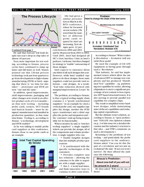
According to Strauss “What it takes<br />
is Revolution – Evolution will not<br />
yield these goals!<br />
He used the example of LSI ATE<br />
equipment as having gone through<br />
such a “Revolution.”<br />
That industry, he said has implemented<br />
testers which allow the use<br />
of advanced DFT to manage test complexity<br />
and has produced “Distributed<br />
<strong>Test</strong>” capability – eg. partitioning<br />
test capability by socket, allowing<br />
chipmakers to move a significant percentage<br />
of test content to less expensive<br />
DFT based structural testers. It is<br />
also moving to provide parallel test<br />
capability for complex chips.<br />
The result is simplified tester hardware<br />
designs, while maintaining<br />
state-of-the-art capabilities and reducing<br />
capital expenditures.<br />
But the ultimate tester solution, according<br />
to Strauss, is “open architecture”<br />
VLSI ATE. (See Opinion column<br />
on p. 3 of this issue for a detailed discussion<br />
and the industry's reaction to<br />
that idea – and FTR's comments on<br />
such a development.)<br />
Returning to the problems of test<br />
tooling – and particularly the probe<br />
card suppliers in the audience.<br />
Strauss asked “Can you do this [be<br />
part of a revolution and not just an<br />
evolution]? He said, “If not you won’t<br />
survive!. He then offered the audience<br />
the following<br />
Strauss’s Prediction :<br />
About one-half of you will not<br />
be around in 2 years!<br />
He then asked “Will you be one of<br />
them?


