Medium range order of bulk metallic glasses determined by variable ...
Medium range order of bulk metallic glasses determined by variable ...
Medium range order of bulk metallic glasses determined by variable ...

You also want an ePaper? Increase the reach of your titles
YUMPU automatically turns print PDFs into web optimized ePapers that Google loves.
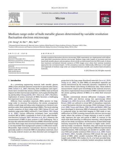
Micron 43 (2012) 827–831<br />
Contents lists available at SciVerse ScienceDirect<br />
Micron<br />
j our na l ho me p age: www.elsevier.com/locate/micron<br />
<strong>Medium</strong> <strong>range</strong> <strong>order</strong> <strong>of</strong> <strong>bulk</strong> <strong>metallic</strong> <strong>glasses</strong> <strong>determined</strong> <strong>by</strong> <strong>variable</strong> resolution<br />
fluctuation electron microscopy<br />
J.W. Deng a , K. Du a,∗ , M.L. Sui b,∗<br />
a Shenyang National Laboratory for Materials Science, Institute <strong>of</strong> Metal Research, Chinese Academy <strong>of</strong> Sciences, Shenyang 110016, China<br />
b Institute <strong>of</strong> Microstructure and Property <strong>of</strong> Advanced Materials, Beijing University <strong>of</strong> Technology, Beijing 100124, China<br />
a r t i c l e i n f o<br />
Article history:<br />
Received 10 November 2011<br />
Received in revised form 10 February 2012<br />
Accepted 10 February 2012<br />
Keywords:<br />
Fluctuation electron microscopy<br />
<strong>Medium</strong>-<strong>range</strong> <strong>order</strong><br />
Bulk <strong>metallic</strong> <strong>glasses</strong><br />
Transmission electron microscopy<br />
a b s t r a c t<br />
Variable resolution fluctuation electron microscopy (FEM) experiments are implemented with hollowcone<br />
dark-field transmission electron microscopy. <strong>Medium</strong> <strong>range</strong> <strong>order</strong> lengths <strong>of</strong> zirconium and iron<br />
based <strong>bulk</strong> <strong>metallic</strong> <strong>glasses</strong> and amorphous silicon nitride are <strong>determined</strong> from the FEM results. It shows<br />
that maximum normalized intensity variances <strong>of</strong> FEM images occur when their nominal resolution<br />
approaches the correlation length <strong>of</strong> the amorphous materials. Additionally, differences in the length<br />
and magnitude <strong>of</strong> medium <strong>range</strong> <strong>order</strong> are compared between <strong>metallic</strong> and covalent bond amorphous<br />
materials.<br />
© 2012 Elsevier Ltd. All rights reserved.<br />
1. Introduction<br />
As a promising engineering material, <strong>bulk</strong> <strong>metallic</strong> <strong>glasses</strong><br />
(BMGs) have attracted intensive researches in past decades (Inoue,<br />
2000; Schuh et al., 2007). Recently, both simulations and experiments<br />
have revealed that atomic schemes <strong>of</strong> BMGs have pr<strong>of</strong>ound<br />
impacts on their macroscopic properties, such as glass forming ability<br />
and ductility (Cheng and Ma, 2011; Wen et al., 2007). Therefore,<br />
exploration <strong>of</strong> atomic structures <strong>of</strong> BMGs becomes a challenging<br />
but important issue in materials science.<br />
Different from crystalline materials, BMGs possess no long<strong>range</strong><br />
<strong>order</strong> in structure. Nevertheless, the atomic ar<strong>range</strong>ment<br />
within a small <strong>range</strong> still obeys rules <strong>of</strong> geometry or chemical composition<br />
rather than randomly packing in BMGs. This local <strong>order</strong>ing<br />
usually comprises <strong>of</strong> short-<strong>range</strong> <strong>order</strong> (SRO) (below 0.5 nm) and<br />
medium-<strong>range</strong> <strong>order</strong> (MRO) (within 0.5–3 nm) (Elliott, 1991; Sheng<br />
et al., 2006). Various diffraction techniques have successfully<br />
resolved SRO <strong>of</strong> BMGs, commonly in form <strong>of</strong> the radial distribution<br />
function (Cockayne, 2007; Wochner et al., 2011). However, the<br />
measurement <strong>of</strong> MRO in glass systems is still challenging. This is<br />
because the radial distribution function <strong>of</strong> BMGs diminishes quickly<br />
out <strong>of</strong> the short <strong>range</strong>, thus structural information at medium <strong>range</strong><br />
is not discernible from background variation in diffraction results.<br />
Meanwhile, high-resolution transmission electron microscopy is<br />
generally unable to reveal the MRO <strong>of</strong> amorphous materials, since<br />
the locally <strong>order</strong>ed clusters are <strong>of</strong>ten distorted and overlapped in<br />
∗ Corresponding authors.<br />
E-mail addresses: kuidu@imr.ac.cn (K. Du), mlsui@bjut.edu.cn (M.L. Sui).<br />
projection in the long-<strong>range</strong> dis<strong>order</strong>ed materials (Lee et al., 2010;<br />
Treacy et al., 2005). To date MROs <strong>of</strong> amorphous materials are<br />
mostly <strong>determined</strong> <strong>by</strong> the molecular dynamics simulation or <strong>by</strong><br />
the reverse Monte Carlo fitting <strong>of</strong> diffraction data. These indirect<br />
measurements require prior knowledge <strong>of</strong> the material structure,<br />
thus direct experimental measurement <strong>of</strong> MRO is desired to reveal<br />
the atomic packing schemes <strong>of</strong> BMGs or to refine their structure<br />
models.<br />
Besides conventional electron diffraction (Cockayne, 2007;<br />
Cowley, 2004) and electron energy loss spectroscopy (EELS)<br />
(Alamgir et al., 2003; Ferrari et al., 2000; Wang et al., 2008; Yuan and<br />
Brown, 2000) are utilized to reveal SRO <strong>of</strong> amorphous materials,<br />
a novel fluctuation electron microscopy (FEM) technique (Gibson<br />
et al., 2000; Treacy and Gibson, 1996; Voyles and Muller, 2002) has<br />
been developed to determine MRO <strong>of</strong> amorphous structures. FEM<br />
is conducted either <strong>by</strong> dark-field imaging in TEM mode or nanodiffraction<br />
in STEM (scanning transmission electron microscopy)<br />
mode, where the variance <strong>of</strong> image intensity is used to statistically<br />
represent the type and extent <strong>of</strong> MRO. In contrast to the<br />
mean dark-field intensity (or diffraction intensity), which depends<br />
only on two-body correlations, the fluctuations <strong>of</strong> dark-field image<br />
intensity measured <strong>by</strong> FEM are sensitive to higher <strong>order</strong> (threeand<br />
four-body) correlations. Therefore, they will reveal structural<br />
<strong>order</strong>ing at the medium <strong>range</strong>. According to different experimental<br />
implementations, FEM techniques are divided to <strong>variable</strong> coherence<br />
FEM and <strong>variable</strong> resolution FEM (Gibson et al., 2000; Voyles<br />
and Muller, 2002). Variable coherence FEM reveals the type and<br />
extent <strong>of</strong> MRO, while <strong>variable</strong> resolution FEM gives mainly the<br />
length scale <strong>of</strong> MRO. FEM studies <strong>of</strong> a-Si, a-Ge have provided helpful<br />
MRO information on covalently bonded amorphous materials<br />
0968-4328/$ – see front matter © 2012 Elsevier Ltd. All rights reserved.<br />
doi:10.1016/j.micron.2012.02.006
828 J.W. Deng et al. / Micron 43 (2012) 827–831<br />
(Treacy et al., 2005; Voyles and Abelson, 2003), and investigations<br />
on BMGs have also illustrated effects <strong>of</strong> minor alloying elements,<br />
structural relaxation, and deformation processes on MRO <strong>of</strong> BMGs<br />
(Li et al., 2003; Stratton et al., 2005; Wen et al., 2007). However,<br />
most <strong>of</strong> reported works are conducted with <strong>variable</strong> coherence<br />
FEM, while only a few <strong>variable</strong> resolution FEM experiments are<br />
preformed in STEM <strong>by</strong> varying the size <strong>of</strong> electron probe (Bogle<br />
et al., 2010; Daulton et al., 2010; Hwang and Voyles, 2011). In<br />
this study, <strong>variable</strong> resolution FEM was implemented in TEM <strong>by</strong><br />
changing the size <strong>of</strong> objective lens aperture, and MRO lengths <strong>of</strong><br />
amorphous materials with different bonding types were obtained.<br />
Additionally, the optimal resolution for FEM experiment is also discussed<br />
based on the situation <strong>of</strong> obtaining the maximum intensity<br />
variance.<br />
2. Experimental<br />
Two Zr-based and one Fe-based BMGs were chosen for<br />
the FEM experiment. Zr 64.13 Cu 15.75 Ni 10.12 Al 10 (Zr-S2) and<br />
Zr 52.5 Ti 5 Cu 17.9 Ni 14.6 Al 10 (Zr-Vit105) samples are plates with<br />
10 mm width and 1 mm thickness. Fe 48 Cr 15 Mo 14 C 15 B 6 Y 2 are rods<br />
with 3 mm in diameter. All <strong>of</strong> the BMG samples were prepared <strong>by</strong><br />
arc melting and copper mold casting. The amorphous structure<br />
<strong>of</strong> BMG samples was confirmed <strong>by</strong> X-ray diffraction and highresolution<br />
transmission electron microscopy. TEM samples were<br />
prepared <strong>by</strong> electropolishing in a Struers Tenupol-5 twin-jet electropolisher<br />
with the electrolyte <strong>of</strong> 10% perchloric acid in ethanol<br />
at 238 K. In <strong>order</strong> to avoid subtle structure changes occurring in<br />
the samples during storage (Stratton et al., 2004), the prepared<br />
TEM specimens were examined within 48 h after thinning. FEM<br />
experiment was also conducted on amorphous silicon nitride<br />
(a-Si 3 N 4 ) membranes <strong>of</strong> commercial TEM grids. The thickness <strong>of</strong><br />
a-Si 3 N 4 foil is 20 nm.<br />
FEM works were performed in hollow-cone illumination mode<br />
on a Tecnai G 2 F30 TEM operated at 200 kV. Details <strong>of</strong> the FEM<br />
experimental procedure are described in a previous paper (Wen<br />
et al., 2007). The variance V(k) curve is obtained from the average<br />
<strong>of</strong> experiment results taken from more than ten different areas in a<br />
sample. To assure the consistence <strong>of</strong> thickness in different sample<br />
areas, the electron transmittance for the selected areas was<br />
examined before acquisition <strong>of</strong> each image series. In this study,<br />
the desired transmittances for Zr-based and Fe-based BMG samples<br />
are 50 ± 2% and 40 ± 2%, respectively, which correspond to a<br />
thickness less than 30 nm. The specimen thicknesses were verified<br />
<strong>by</strong> using the log-ratio method based on EELS (Egerton, 1996). The<br />
thicknesses were below 0.3 multiplies <strong>of</strong> the inelastic mean free<br />
path in the 50% and 40% electron transmittance areas. The inelastic<br />
mean free paths for the Zr-based and Fe-based samples are about<br />
82 and 91 nm, respectively, calculated <strong>by</strong> using the DigitalMicrograph<br />
script <strong>of</strong> Mean Free Path Estimator (Mitchell, 2006) based<br />
on Malis method (Malis et al., 1988). The magnification and the<br />
pixel size <strong>of</strong> the images are kept constant for all samples and all the<br />
resolutions during the experiment. To compensate the low image<br />
intensity <strong>of</strong> smaller aperture, longer acquisition time is applied.<br />
The mean intensity <strong>of</strong> each dark-field image at different k values<br />
(obtained <strong>by</strong> changing the tilt angle <strong>of</strong> the incident electron beam)<br />
is also kept constant <strong>by</strong> adjusting the collection time. The highest<br />
k for FEM curves was chosen appropriately (8 nm −1 for BMGs<br />
and 7.3 nm −1 for a-Si 3 N 4 ) to avoid too low image intensity in the<br />
high k region. In this work, the longest acquisition time for single<br />
image has not exceeded 30 s in the highest k and with the smallest<br />
aperture. Although a long exposure time may bring artifacts<br />
into hollow-cone dark-field images due to such as specimen drift,<br />
instrumental instability, and CCD shot noise, these effects have not<br />
shown significant influences on the results when the acquisition<br />
Fig. 1. Select area electron diffraction pattern <strong>of</strong> Zr-S2 BMG sample. The insets are<br />
images <strong>of</strong> different objective apertures in the diffraction plane, while the scale bars<br />
are same as that <strong>of</strong> the diffraction pattern.<br />
Table 1<br />
Parameters <strong>of</strong> objective apertures used in the experiment. Q and R denote radii <strong>of</strong> the<br />
apertures in reciprocal space and nominal resolutions <strong>of</strong> FEM images, respectively.<br />
Aperture size (m) Q (nm −1 ) R (nm)<br />
5 0.55 1.1<br />
10 1.0 0.6<br />
20 2.3 0.3<br />
time is less than 30 s. The data acquisition and image processing<br />
were implemented on the DigitalMicrograph s<strong>of</strong>tware using script<br />
programs (Wen et al., 2007). The variance V(k,Q) <strong>of</strong> dark-field image<br />
is calculated as,<br />
〈 〉 I 2 (k, Q )<br />
V(k, Q ) = 〈 〉 2 − 1 (1)<br />
I(k, Q )<br />
where k is the scattering vector, and Q is the radius <strong>of</strong> the objective<br />
aperture in reciprocal space. 〈I 2 (k,Q)〉 and 〈I(k,Q)〉 are the mean<br />
square intensity and averaged intensity <strong>of</strong> the dark-field image,<br />
respectively.<br />
An objective aperture strip with a series <strong>of</strong> aperture sizes was<br />
used to carry out the <strong>variable</strong> resolution FEM. The objective aperture<br />
strip was <strong>order</strong>ed from Ladd Research Inc. (Williston, VT, USA).<br />
The Pt aperture strip contains circular apertures with different<br />
diameters and aperture diameters <strong>of</strong> 5, 10 and 20 m were used<br />
in this work. A select area electron diffraction pattern <strong>of</strong> the Zr-<br />
S2 sample is presented in Fig. 1. The halo ring demonstrates that<br />
the specimen is fully amorphous. The insets in Fig. 1 are images<br />
<strong>of</strong> 3 different objective apertures in TEM. By measuring reciprocal<br />
radii Q <strong>of</strong> the circular objective apertures, we have <strong>determined</strong><br />
nominal resolutions <strong>of</strong> the dark-field imaging via R = 0.61/Q (Gibson<br />
et al., 2000) for different apertures. The measured Q and calculated<br />
R values for the apertures are listed in Table 1.<br />
3. Results<br />
Fig. 2 shows the normalized intensity variance V(k) taken at<br />
different scattering vector k from the Zr-S2 sample with FEM.<br />
The scattering vector k was controlled <strong>by</strong> tilting the incident
J.W. Deng et al. / Micron 43 (2012) 827–831 829<br />
Fig. 2. The normalized intensity variance curves <strong>of</strong> Zr-S2 BMG obtained <strong>by</strong> <strong>variable</strong><br />
resolution FEM with different nominal resolutions R.<br />
electron beam against the optic axis with angle (k = sin/, <br />
is the electron wavelength). As the tiled incident beam is continually<br />
rotating around the optic axis, the obtained hollow-cone<br />
dark-filed image is a superposition <strong>of</strong> dark-field images over 360 ◦<br />
azimuth angle at the given k. A series <strong>of</strong> these images were obtained<br />
with k varying from 2.8 to 8.0 nm −1 for each objective aperture.<br />
For the corresponding nominal resolution R (1.1, 0.6, and 0.3 nm,<br />
respectively), a variance V(k) curve was obtained subsequently. The<br />
maximum V(k) located at k = 3.8 nm −1 for all the V(k) curves, where<br />
k = 3.8 nm −1 corresponds to the maximal diffraction intensity in<br />
the electron diffraction patterns (see e.g. Fig. 1). Although these<br />
curves possess similar tendency and peak positions, their maximum<br />
variance values are considerably different. For the nominal<br />
resolution R <strong>of</strong> 0.6 nm, the maximum V(k) is 0.022; while for resolutions<br />
R = 1.1 and 0.3 nm, the maximum V(k) are 0.0094 and 0.017,<br />
respectively. Since the sample and imaging conditions are kept constant<br />
during the experiment, these differences in the maximum<br />
variance are assumed mainly due to the different nominal resolutions<br />
employed. This is also visible in the corresponding dark-field<br />
images. Fig. 3a–c are hollow-cone dark-field images acquired at<br />
the V(k) peak position (k = 3.8 nm −1 ) while the 1.1, 0.6, and 0.3 nm<br />
nominal resolutions were used, respectively. All <strong>of</strong> the images are<br />
collected and shown with the same intensity scale for comparison.<br />
The speckle contrast in Fig. 3b is clear when the 0.6 nm resolution<br />
was used, while they are blurred when the other two resolutions<br />
were employed. V(k) curve in the lower k region for the 0.3 nm<br />
resolution is absent in Fig. 2, this is because the transmitted beam<br />
was partly included in the lower k region when a large aperture<br />
is used. Nevertheless, a V(k) peak is clearly visible in the variance<br />
curve for the Fe-based BMG sample with the 0.3 nm resolution (as<br />
shown in Fig. 4a). For comparison, normalized intensity variance<br />
curves for a-Si 3 N 4 are also presented in Fig. 4b. The maximum<br />
V(k) at each nominal resolution R are summarized in Fig. 5 for all<br />
the amorphous samples (Zr-S2, Zr-Vit105, Fe-based BMG, and a-<br />
Si 3 N 4 ). Noticeably, the variation <strong>of</strong> the maximum V(k) values with<br />
the nominal resolution follows the same tendency for the different<br />
Fig. 3. (a)–(c) Hollow-cone dark-field images <strong>of</strong> Zr-S2 BMG sample acquired at the peak V(k) position (k = 3.8 nm −1 ) with different nominal resolutions R ((a) 1.1 nm, (b)<br />
0.6 nm, and (c) 0.3 nm).<br />
Fig. 4. The normalized intensity variance curves <strong>of</strong> (a) Fe-based BMG and (b) a-Si 3N 4 samples obtained <strong>by</strong> <strong>variable</strong> resolution FEM with different nominal resolutions R.
830 J.W. Deng et al. / Micron 43 (2012) 827–831<br />
Fig. 5. Summary <strong>of</strong> the peak variance V(k) values obtained using different nominal<br />
resolutions R for all tested amorphous materials.<br />
Table 2<br />
Correlation lengths and characteristic widths W <strong>of</strong> the amorphous materials. The<br />
mean atomic radii, r, <strong>of</strong> the materials are listed, as well as ratios /r between the<br />
correlation lengths and the mean atomic radii.<br />
(nm) W (nm) r (nm) /r<br />
a-Si 3N 4 0.69 ± 0.055 2.2 0.096 7.2<br />
Zr-S2 0.81 ± 0.35 2.6 0.15 5.4<br />
Zr-Vit105 0.85 ± 0.34 2.7 0.15 5.7<br />
Fe-BMG 0.88 ± 0.11 2.8 0.13 6.8<br />
amorphous materials, and the greatest V(k) were obtained with the<br />
0.6 nm resolution.<br />
4. Discussion<br />
4.1. MRO length <strong>of</strong> the amorphous materials<br />
The major advantage <strong>of</strong> <strong>variable</strong> resolution FEM is that it semiquantitatively<br />
determines MRO length <strong>of</strong> amorphous materials<br />
with no needs <strong>of</strong> prior knowledge on the material structure. By the<br />
use <strong>of</strong> pair persistence model (Gibson et al., 2000), the correlation<br />
lengths <strong>of</strong> the amorphous materials can be <strong>determined</strong> from the<br />
<strong>variable</strong> resolution FEM results. By assuming that the four-body<br />
atom correlation function g 4 has a Gaussian decay envelope, the<br />
variance V(k,Q) is transformed into following expression,<br />
(<br />
Q 2<br />
V(k, Q ) =<br />
1<br />
3 P(k)<br />
)<br />
+<br />
( 4 2<br />
P(k)<br />
)<br />
Q 2 . (2)<br />
is correlation decay length, which is closely related with the MRO<br />
length. The structure information independent on MRO length is<br />
separated into P(k), which is a pair persistence function. Accordingly,<br />
a linear correlation can be derived between Q 2 /V(k,Q) and<br />
Q 2 in low resolution (i.e. comparable to the MRO length scale <strong>of</strong><br />
amorphous materials), and the correlation length is obtained as<br />
= 1 √ m<br />
2 c , (3)<br />
where m = 4 2 /P(k) and c = 1/ 3 P(k) are the slope and intercept <strong>of</strong><br />
the linear fitting <strong>of</strong> Q 2 /V(k,Q) against Q 2 (Fig. 6). Correlation lengths<br />
<strong>of</strong> the amorphous materials are presented in Table 2, where<br />
correlation lengths <strong>of</strong> BMGs are between 0.81 nm and 0.88 nm,<br />
which are considerably larger than that <strong>of</strong> a-Si 3 N 4 (∼0.69 nm).<br />
The measured correlation lengths are commonly significant<br />
smaller than the acknowledged MRO lengths in amorphous materials.<br />
A characteristic width W for MRO was proposed as W = √ 10<br />
Fig. 6. Plot <strong>of</strong> the calculated Q 2 /V(k) against Q 2 values for all the amorphous materials<br />
according to the <strong>variable</strong> resolution FEM results. Here the V(k) values were chosen<br />
from Fig. 5. The corresponding Q values were listed in Table 1. Straight lines in different<br />
colors represent linear fitting to the data points. Using the slope and intercept<br />
<strong>of</strong> each fitting line, the correlation lengths <strong>of</strong> tested amorphous materials were<br />
extracted.<br />
<strong>by</strong> assuming as a radius <strong>of</strong> gyration for the correlated spheroidal<br />
<strong>order</strong>ed region (Gibson et al., 2000). In this work, W would be<br />
between 2.6 and 2.8 nm for BMGs, and ∼2.2 nm for a-Si 3 N 4 , which<br />
lies in the reported MRO <strong>range</strong> (0.5–3 nm) (Table 2).<br />
It is noteworthy that the pair persistence model predicts a<br />
monotonically decreasing V with the increase <strong>of</strong> R, which is inconsistent<br />
with our experimental results. Nevertheless, in <strong>order</strong> to<br />
compare with previous reported FEM results, we still used this<br />
method for the calculation <strong>of</strong> correlation lengths in this work.<br />
The obtained correlation lengths <strong>of</strong> a-Si 3 N 4 (0.69 nm) and BMGs<br />
(0.81–0.88 nm) are consistent with correlation lengths <strong>of</strong> amorphous<br />
materials <strong>determined</strong> in previous researches (e.g. 0.3–0.6 nm<br />
for a-Si (Bogle et al., 2010), 0.6–0.9 for CuZr (Hwang and Voyles,<br />
2011)). Therefore, the calculation is reliable, although better understanding<br />
<strong>of</strong> the experimental results would need more advanced<br />
computation models as suggested <strong>by</strong> Stratton and Voyles (2008).<br />
4.2. Size effect <strong>of</strong> objective aperture on the normalized intensity<br />
variance <strong>of</strong> FEM images<br />
As presented in Fig. 5, the highest variance V(k) peaks were all<br />
obtained when 0.6 nm resolution was employed (corresponding<br />
to 10 m objective aperture) for the amorphous samples in this<br />
work. This is probably due to the following reasons. In dark-field<br />
TEM imaging, the bright speckles arise from local <strong>order</strong>ed regions<br />
where coherent diffractions take place between structurally correlated<br />
atoms. In <strong>variable</strong> resolution FEM, the size <strong>of</strong> objective<br />
aperture determines the microscopy resolution in real space (proportional<br />
to 1/Q), which sets a lateral limit that the structurally<br />
<strong>order</strong>ed atoms can interfere coherently within. In this way, the size<br />
<strong>of</strong> objective aperture changes the sampling volume <strong>of</strong> dark-field<br />
imaging (Treacy and Gibson, 1996; Treacy et al., 2005). When the<br />
aperture size is appropriate, the obtained intensity variance value<br />
will reach a maximum because the sampling volume is comparable<br />
to the size <strong>of</strong> <strong>order</strong>ed region so that all structurally correlated<br />
atoms are contained in the sampling volume. A larger sampling<br />
volume (corresponding to smaller aperture) will include atoms outside<br />
an <strong>order</strong>ed region, thus decrease the obtained variance due<br />
to their incoherent interference. In contrast, a smaller sampling<br />
volume (larger aperture) will probe each <strong>order</strong>ed region multiple<br />
times, which also diminishes the variance value according to the
J.W. Deng et al. / Micron 43 (2012) 827–831 831<br />
statistical feature <strong>of</strong> variance (Treacy, 2007; Treacy et al., 2005;<br />
Voyles and Abelson, 2003).<br />
Small objective apertures, which bring the nominal resolution R<br />
to the MRO length scale (0.5–3 nm), were suggested for FEM experiments<br />
to obtain reliable results (Treacy, 2007; Treacy et al., 2005).<br />
In this work, the correlation length is between 0.69 and 0.88 nm,<br />
while the characteristic width W is between 2.2 and 2.8 nm. This<br />
indicates that the maximum variance is obtained when the nominal<br />
resolution R approaches the correlation length rather than<br />
the characteristic width <strong>of</strong> MRO. This consists with recent <strong>variable</strong><br />
resolution FEM experiment on Cu–Zr <strong>metallic</strong> glass in the STEM<br />
nanodiffraction mode (Hwang and Voyles, 2011). By changing the<br />
probe size, FEM resolution was adjusted in STEM. Their results show<br />
that the maximum variance values increase monotonically as the<br />
resolution goes down to 0.8 nm, which is significantly smaller than<br />
the MRO length usually accepted but close to the correlation length<br />
<strong>of</strong> their samples (0.68–0.89 nm). Unfortunately, since there is<br />
no experiment results for even smaller probe size, the downward<br />
trend <strong>of</strong> variance V(k) is not available for further decrease <strong>of</strong> the<br />
resolution in STEM.<br />
Compared with previous FEM works on a-Si, a-Ge, etc., much<br />
smaller resolutions have been used for the BMG and a-Si 3 N 4 samples<br />
in this study and these resolutions work adequately for the<br />
samples. Nevertheless, since different amorphous materials may<br />
have different MRO length scales, the appropriate resolution for<br />
samples in this work might not be the optimum condition for other<br />
materials. Hence, it is necessary to resolve the appropriate resolution<br />
for studied materials prior to conducting FEM experiments in<br />
TEM as suggested <strong>by</strong> Treacy (2007). This is in fact also a motivation<br />
for us to conduct the <strong>variable</strong> resolution FEM study here.<br />
4.3. Comparison between MROs <strong>of</strong> <strong>metallic</strong> and covalent bond<br />
amorphous materials<br />
Although quantitative comparison <strong>of</strong> FEM results between different<br />
materials is hard due to influences from such as sample<br />
thickness, imaging conditions (Daulton et al., 2010; Yi and Voyles,<br />
2011), a preliminary comparison <strong>of</strong> MRO lengths and magnitudes<br />
between covalent bond a-Si 3 N 4 and <strong>metallic</strong> bond BMGs is still<br />
possible especially when experiment configuration was kept consistent.<br />
Firstly, the variance peaks <strong>of</strong> BMGs are greater than that <strong>of</strong><br />
a-Si 3 N 4 as shown in Fig. 5. Since the variance value corresponds<br />
to the extent <strong>of</strong> structural <strong>order</strong>ing, the greater variance indicates<br />
a higher <strong>order</strong>ing or an inhomogeneity in the BMG samples. Secondly,<br />
the correlation lengths <strong>of</strong> BMGs (0.81–0.88 nm) are larger<br />
than that <strong>of</strong> a-Si 3 N 4 (0.69 nm). However, in <strong>order</strong> to compare the<br />
MRO length in a relative scale, each correlation length was<br />
divided <strong>by</strong> the mean atomic radius r <strong>of</strong> the amorphous material<br />
(Table 2). Here, the mean atomic radius was calculated from Goldschmidt<br />
atomic radii <strong>of</strong> elements and chemical composition <strong>of</strong> each<br />
material (Gale and Totemeier, 2004). Although a-Si 3 N 4 has a much<br />
smaller correlation length, its /r value is in fact similar to or even<br />
slightly larger than that <strong>of</strong> BMGs.<br />
The spatial heterogeneity/homogeneity <strong>of</strong> BMGs on the nanoscale<br />
is also an interesting research topic. Researchers have<br />
suggested that the heterogeneity in BMG can play an important role<br />
during the initiation <strong>of</strong> shear bands and the subsequently plastic<br />
deformation process (Murali et al., 2011; Wang et al., 2012). However,<br />
the main focus <strong>of</strong> present work is to determine the length scale<br />
<strong>of</strong> medium <strong>range</strong> <strong>order</strong> in different amorphous materials. In <strong>order</strong><br />
to reveal the structure character <strong>of</strong> heterogeneity in BMGs, which<br />
is beyond the scope <strong>of</strong> this work, more experiments and analysis<br />
would be needed.<br />
5. Conclusions<br />
Variable resolution FEM has been successfully performed in<br />
TEM <strong>by</strong> varying the objective aperture size in a hollow-cone darkfield<br />
imaging mode on <strong>metallic</strong> and covalent bond amorphous<br />
materials. Correlation lengths <strong>of</strong> = 0.69 nm for covalently bonded<br />
a-Si 3 N 4 and = 0.81–0.88 nm for BMGs were extracted <strong>by</strong> fitting<br />
the variance values at different resolution situations. The experiment<br />
reveals that maximum intensity variance was obtained when<br />
the nominal resolution <strong>of</strong> FEM images approaches the correlation<br />
length <strong>of</strong> the studied amorphous materials.<br />
Acknowledgments<br />
The authors thank B. Wu for technical supports and F.F. Wu,<br />
Q.P. Cao and J.Z. Jiang for sample preparation. The authors would<br />
also like to thank the Hundred Talents Project <strong>of</strong> Chinese Academy<br />
<strong>of</strong> Sciences, the Cheung Kong Scholars Programme <strong>of</strong> China, the<br />
Natural Sciences Foundation <strong>of</strong> China (Grant Nos. 50671104 and<br />
50921004) and the Special Funds for the Major State Basic Research<br />
Projects <strong>of</strong> China (Grant No. 2009CB623705) for the financial support.<br />
References<br />
Alamgir, F.A., Jain, H., Williams, D.B., Schwarz, R.B., 2003. Micron 34, 433.<br />
Bogle, S.N., Nittala, L.N., Twesten, R.D., Voyles, P.M., Abelson, J.R., 2010. Ultramicroscopy<br />
110, 1273.<br />
Cheng, Y.Q., Ma, E., 2011. Prog. Mater. Sci. 56, 379.<br />
Cockayne, D.J.H., 2007. Annu. Rev. Mater. Res. 37, 159.<br />
Cowley, J.M., 2004. Micron 35, 345.<br />
Daulton, T.L., Bondi, K.S., Kelton, K.F., 2010. Ultramicroscopy 110, 1279.<br />
Egerton, R.F., 1996. Electron Energy-Loss Spectroscopy in the Electron Microscope,<br />
2nd ed. Plenum Press, New York.<br />
Elliott, S.R., 1991. Nature 354, 445.<br />
Ferrari, A.C., Libassi, A., Tanner, B.K., Stolojan, V., Yuan, J., Brown, L.M., Rodil, S.E.,<br />
Kleinsorge, B., Robertson, J., 2000. Phys. Rev. B 62, 11089.<br />
Gale, W.F., Totemeier, T.C., 2004. Smithells Metals Reference Book, 8th ed.<br />
Butterworth-Heinemann, Oxford.<br />
Gibson, J.M., Treacy, M.M.J., Voyles, P.M., 2000. Ultramicroscopy 83, 169.<br />
Hwang, J., Voyles, P.M., 2011. Microsc. Microanal. 17, 67.<br />
Inoue, A., 2000. Acta Mater. 48, 279.<br />
Lee, B.S., Bishop, S.G., Abelson, J.R., 2010. Chemphyschem 11, 2311.<br />
Li, J., Gu, X., Hufnagel, T.C., 2003. Microsc. Microanal. 9, 509.<br />
Malis, T., Cheng, S.C., Egerton, R.F., 1988. J. Electron Microsc. Tech. 8, 193.<br />
Mitchell, D.R.G., 2006. J. Microsc. 224, 187.<br />
Murali, P., Guo, T.F., Zhang, Y.W., Narasimhan, R., Li, Y., Gao, H.J., 2011. Phys. Rev.<br />
Lett. 107, 215501.<br />
Schuh, C.A., Hufnagel, T.C., Ramamurty, U., 2007. Acta Mater. 55, 4067.<br />
Sheng, H.W., Luo, W.K., Alamgir, F.M., Bai, J.M., Ma, E., 2006. Nature 439, 419.<br />
Stratton, W.G., Hamann, J., Perepezko, J.H., Voyles, P.M., 2004. <strong>Medium</strong>-<strong>range</strong><br />
<strong>order</strong> in high Al-content amorphous alloys measured <strong>by</strong> fluctuation electron<br />
microscopy. In: Busch, R., Hufnagel, T.C., Eckert, J., Inoue, A., Johnson, W.L., Yavari,<br />
A.R. (Eds.), Amorphous and Nanocrystalline Metals. Materials Research Society,<br />
Warrendale, p. 275.<br />
Stratton, W.G., Hamann, J., Perepezko, J.H., Voyles, P.M., Mao, X., Khare, S.V., 2005.<br />
Appl. Phys. Lett. 86, 141910.<br />
Stratton, W.G., Voyles, P.M., 2008. Ultramicroscopy 108, 727.<br />
Treacy, M.M.J., 2007. Ultramicroscopy 107, 166.<br />
Treacy, M.M.J., Gibson, J.M., 1996. Acta Crystallogr. A 52, 212.<br />
Treacy, M.M.J., Gibson, J.M., Fan, L., Paterson, D.J., McNulty, I., 2005. Rep. Prog. Phys.<br />
68, 2899.<br />
Voyles, P.M., Abelson, J.R., 2003. Sol. Energy Mater. Sol. Cells 78, 85.<br />
Voyles, P.M., Muller, D.A., 2002. Ultramicroscopy 93, 147.<br />
Wang, H.J., Gu, X.J., Poon, S.J., Shiflet, G.J., 2008. Phys. Rev. B 77, 014204.<br />
Wang, Y.B., Qu, D.D., Wang, X.H., Cao, Y., Liao, X.Z., Kawasaki, M., Ringer, S.P., Shan,<br />
Z.W., Langdon, T.G., Shen, J., 2012. Acta Mater. 60, 253.<br />
Wen, J., Yang, H.W., Guo, H., Wu, B., Sui, M.L., Wang, J.Q., Ma, E., 2007. J. Phys.:<br />
Condens. Matter 19, 455211.<br />
Wochner, P., Castro-Colin, M., Bogle, S.N., Bugaev, V.N., 2011. Int. J. Mater. Res. 102,<br />
874.<br />
Yi, F., Voyles, P.M., 2011. Ultramicroscopy 111, 1375.<br />
Yuan, J., Brown, L.M., 2000. Micron 31, 515.