F35-XXL Hardware description - Falcom
F35-XXL Hardware description - Falcom
F35-XXL Hardware description - Falcom

Create successful ePaper yourself
Turn your PDF publications into a flip-book with our unique Google optimized e-Paper software.
This document is available at HTTP://WWW.FALCOM.DE/.<br />
Version 1.10<br />
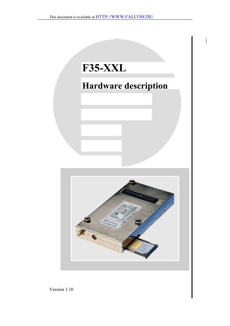
<strong>F35</strong>-<strong>XXL</strong><br />
<strong>Hardware</strong> <strong>description</strong>
<strong>F35</strong>-<strong>XXL</strong> HARDWARE DESCRIPTION VERSION 1.10<br />
Contents<br />
0 INTRODUCTION ..............................................................4<br />
0.1 GENERAL........................................................................................................................................ 4<br />
0.2 USED ABBREVIATIONS.................................................................................................................... 6<br />
0.3 RELATED DOCUMENTS.................................................................................................................... 8<br />
1 SECURITY .........................................................................9<br />
1.1 GENERAL INFORMATION................................................................................................................. 9<br />
1.2 EXPOSURE TO RF ENERGY.............................................................................................................. 9<br />
1.3 EFFICIENT MODEM OPERATION....................................................................................................... 9<br />
1.4 ANTENNA CARE AND REPLACEMENT ............................................................................................ 10<br />
1.5 DRIVING ....................................................................................................................................... 10<br />
1.6 ELECTRONIC DEVICES................................................................................................................... 10<br />
1.7 VEHICLE ELECTRONIC EQUIPMENT ............................................................................................... 10<br />
1.8 MEDICAL ELECTRONIC EQUIPMENT .............................................................................................. 10<br />
1.9 AIRCRAFT..................................................................................................................................... 10<br />
1.10 CHILDREN .................................................................................................................................... 11<br />
1.11 BLASTING AREAS.......................................................................................................................... 11<br />
1.12 POTENTIALLY EXPLOSIVE ATMOSPHERES ..................................................................................... 11<br />
1.13 NON-IONISING RADIATION............................................................................................................ 11<br />
2 SAFETY STANDARDS...................................................12<br />
3 TECHNICAL DATA........................................................13<br />
4 PIN ASSIGNMENT AND SIGNAL LEVELS...............15<br />
5 GSM CORE ......................................................................25<br />
5.1 TECHNICAL DATA......................................................................................................................... 25<br />
5.1.1 General......................................................................................................................................... 25<br />
5.1.2 Features........................................................................................................................................ 25<br />
5.2 HARDWARE INTERFACE................................................................................................................ 27<br />
5.2.1 Interface for external 3 V SIM card reader.................................................................................. 27<br />
5.2.2 Audio interface ............................................................................................................................ 28<br />
5.2.3 Serial interface............................................................................................................................. 28<br />
5.2.4 Control signals............................................................................................................................. 29<br />
5.2.4.1 Ring- MC39i................................................................................................................................................. 29<br />
5.2.4.2 SYNC to control a status LED...................................................................................................................... 31<br />
5.2.5 General propose input/output....................................................................................................... 32<br />
5.2.6 General pin configuration ............................................................................................................ 32<br />
6 GPS CORE........................................................................34<br />
6.1 TECHNICAL DATA......................................................................................................................... 34<br />
6.2 TECHNICAL DESCRIPTION............................................................................................................. 36<br />
6.2.1 Receiver Architecture .................................................................................................................. 36<br />
6.2.2 Technical specification ................................................................................................................ 37<br />
6.3 HARDWARE INTERFACE................................................................................................................ 38<br />
6.3.1 Configuration and timing signals................................................................................................. 38<br />
6.3.2 Serial communication signals ...................................................................................................... 38<br />
6.3.3 DC input signals .......................................................................................................................... 40<br />
6.3.4 General purpose input/output (pin 81, 110, 112, 114 and 116) ................................................... 40<br />
6.4 SOFTWARE INTERFACE ................................................................................................................. 40<br />
6.4.1 SiRF binary data message............................................................................................................ 41<br />
6.4.2 NMEA data message ................................................................................................................... 43<br />
6.4.2.1 NMEA output messages................................................................................................................................ 43<br />
6.4.2.2 NMEA input messages.................................................................................................................................. 44<br />
This confidential document is the property of FALCOM GmbH and may not be copied or circulated without permission.<br />
Page 1
<strong>F35</strong>-<strong>XXL</strong> HARDWARE DESCRIPTION VERSION 1.10<br />
7 PROCESSOR CORE .......................................................46<br />
7.1 HOW TO USE THE TCP/IP AND PPP STACK................................................................................... 50<br />
8 GETTING STARTED......................................................51<br />
8.1 DETERMINING THE EXTERNAL EQUIPMENT TYPE......................................................................... 51<br />
8.2 MINIMUM HARDWARE INTERFACE TO GET STARTED..................................................................... 52<br />
9 HOUSING .........................................................................53<br />
10 EMC AND ESD REQUIREMENT.................................55<br />
11 CE CONFORMITY .........................................................56<br />
12 EVALUATION BOARD FOR <strong>F35</strong>-<strong>XXL</strong> .......................57<br />
13 EVALUATION KIT (EVAL-KIT) .................................64<br />
14 APPENDIX .......................................................................65<br />
14.1 HOW TO PUT THE <strong>F35</strong>-<strong>XXL</strong>(SI) INTO THE SLEEP MODE?............................................................. 65<br />
14.2 HOW TO COMMUNICATE WITH EXTRA EXTERNAL I2C DEVICES? .................................................. 65<br />
14.3 HOW TO UPDATE PROGRAMMATICALLY YOUR SOFTWARE INTO THE FLASH? ............................. 65<br />
14.4 HOW ARE THE PINS OF 120-PIN CONNECTOR CONNECTED TO THE NEC V850?............................. 65<br />
14.5 EVAL-BOARD CIRCUIT DIAGRAM............................................................................................. 68<br />
14.6 EVAL-BOARD PIN OUT.............................................................................................................. 70<br />
This confidential document is the property of FALCOM GmbH and may not be copied or circulated without permission.<br />
Page 2
<strong>F35</strong>-<strong>XXL</strong> HARDWARE DESCRIPTION VERSION 1.10<br />
Version history:<br />
Version number Author Changes<br />
1.00 Gerald Buch Initial version<br />
1.01 Fadil Beqiri General, User abbreviation, Technical data,<br />
Housing, Evaluation Board for <strong>F35</strong>-<strong>XXL</strong>,<br />
Evaluation Kit (EVAL-KIT), Circuit diagram, Pin<br />
out.<br />
1.02 Fadil Beqiri<br />
1.03 Fadil Beqiri<br />
1.04 Fadil Beqiri<br />
1.05 Fadil Beqiri<br />
1.06 Fadil Beqiri − Misprints corrected.<br />
1.07 Fadil Beqiri<br />
1.08 Fadil Beqiri<br />
1.09 Fadil Beqiri<br />
1.10 Fadil Beqiri<br />
− GPS-receiver (power consumption and DC<br />
power) (G. Voigt)<br />
− RAM-chip changed to SRAM-chip (G. Voigt)<br />
− Figure 11 (default settings for trickle power<br />
mode) (G. Voigt)<br />
− Type of 120-pin connector (B. Kirchner)<br />
− In chapter 3, pin 46 (V_ANT) will be available<br />
for Power Supply to external GPS antenna (B.<br />
Kirchner).<br />
− Counterpart of the 120-pin connector changed.<br />
− The current <strong>F35</strong>-<strong>XXL</strong>(-SI) module are supplied<br />
with MC39i GSM/GPRS module instead of<br />
MC35 module.<br />
− Pin 98 and pin 100 (GPS part) updated.<br />
− Some source code example are added<br />
− Eval-Board circuit diagram updated.<br />
− The <strong>description</strong> of pin 63 (PWR_GOOD) on the<br />
chapter 5.2.6 updated.<br />
− In chapter 3, external V_ANT pin is a hardware<br />
option only.<br />
− In chapter 6.3.2 the corresponding pin number of<br />
RxDA, RxDB and TxDA, TxDB on the board to<br />
board connector updated.<br />
− The Pin 108 (TMARK) changed to GPOX7<br />
(UART RSTD)<br />
− The GSM/GPRS core MC35i replaced by the<br />
MC39i GSM/GPRS engine. For detailed<br />
information refer to the related documents [1.]<br />
and [2.] available on the FALCOM’s website.<br />
This confidential document is the property of FALCOM GmbH and may not be copied or circulated without permission.<br />
Page 3
<strong>F35</strong>-<strong>XXL</strong> HARDWARE DESCRIPTION VERSION 1.10<br />
0 Introduction<br />
0.1 General<br />
The <strong>F35</strong>-<strong>XXL</strong> concept combines 32 bit CPU core, Dual Band GSM engine,<br />
12 channel GPS receiver, 2 audio interfaces (on the 120pin-connector), 8<br />
digital I/Os and 8 digital or analogue inputs. The 1 MB SRAM- and 1 MB<br />
Flash-memory (optional 2+2) on board allow the creation of a large variety<br />
of applications including extensive data logging.<br />
The eCos system software builds the basis for quick and easy development<br />
of your own application firmware using high level programming languages<br />
(GNU tools). The external access to the internal system bus can be used for<br />
debugging purposes as well as for your own hardware extensions. The<br />
ability to update your own application firmware over the air link reduces<br />
time and cost for field testing and after sales support providing very high<br />
flexibility in responding to the dynamic range of end user requirements.<br />
Thus the <strong>F35</strong>-<strong>XXL</strong> concept brings together powerful state-of-the art<br />
technologies (GSM, GPS, internet) and makes them available for quick and<br />
easy integration into a number of applications for the vertical and horizontal<br />
market.<br />
The table below shows the combination versions of the <strong>F35</strong>-<strong>XXL</strong>-basis.<br />
DEVICE DISCRIPTION AVAILABILITY<br />
<strong>F35</strong>-<strong>XXL</strong>-SI-G8-1<br />
<strong>F35</strong>-<strong>XXL</strong>-SI-G8-2<br />
<strong>F35</strong>-<strong>XXL</strong>-G8-1<br />
<strong>F35</strong>-<strong>XXL</strong>-G8-2<br />
GSM/GPRS Class B/multi-slot class 10/GPS<br />
1 MB SRAM, 1 MB FLASH<br />
GSM/GPRS Class B/multi-slot class 10/GPS<br />
2 MB SRAM, 2 MB FLASH<br />
GSM/GPRS Class B/multi-slot class 10<br />
1 MB SRAM, 1 MB FLASH<br />
GSM/GPRS Class B/multi-slot class 10<br />
2 MB SRAM, 2 MB FLASH<br />
Now<br />
Available soon<br />
Now<br />
Available soon<br />
This confidential document is the property of FALCOM GmbH and may not be copied or circulated without permission.<br />
Page 4
<strong>F35</strong>-<strong>XXL</strong> HARDWARE DESCRIPTION VERSION 1.10<br />
Figure 1: Architecture of the <strong>F35</strong>-<strong>XXL</strong>-SI<br />
Figure 2: View of the Bottom- Side of the <strong>F35</strong>-<strong>XXL</strong>- Motherboard<br />
This confidential document is the property of FALCOM GmbH and may not be copied or circulated without permission.<br />
Page 5
<strong>F35</strong>-<strong>XXL</strong> HARDWARE DESCRIPTION VERSION 1.10<br />
Figure 3: View of the Top- Side of the <strong>F35</strong>-<strong>XXL</strong>- Motherboard<br />
0.2 Used abbreviations<br />
Abbreviation Description<br />
CTS Clear to send<br />
DGPS Differential GPS<br />
DOP Dilution of Precision<br />
DSR Data Set Ready<br />
DTR Data Terminal Ready<br />
DCD Data Carrier Detect<br />
ECEF Earth-Centred Earth-Fixed Co-ordinate system<br />
EEPROM Memory for parameter<br />
EGSM Enhanced GSM<br />
ESD Electrostatic Discharge<br />
ETS European Telecommunication Standard<br />
GPRS General Packet Radio Service<br />
GPS Global Positioning System<br />
GSM Global Standard for Mobile Communications<br />
This confidential document is the property of FALCOM GmbH and may not be copied or circulated without permission.<br />
Page 6
<strong>F35</strong>-<strong>XXL</strong> HARDWARE DESCRIPTION VERSION 1.10<br />
Abbreviation Description<br />
GGA GPS Fixed Data<br />
HDOP Horizontal DOP<br />
HW <strong>Hardware</strong><br />
IMEI International Mobile Equipment Identity<br />
I/O Input/Output<br />
NMEA National Maritime Electronics Association<br />
PRN Pseudorandom Noise Number – The Identity of GPS satellites<br />
RF Radio Frequency<br />
RI Ring Indication<br />
RP Receive Protocol<br />
RTC Real Time Clock<br />
RTCM Radio Technical Commission for Maritime Services<br />
RTS Ready To Send<br />
Rx Receive direction<br />
RXD Data input<br />
RXQUAL Received Signal Quality<br />
SIM Subscriber Identification Module<br />
SMS Short Message Service<br />
SRAM Static Random Access Memory<br />
SW Software<br />
TA Terminal Adapter<br />
TE Terminal Equipment<br />
TP Transmit Protocol<br />
TTFF Time to First Fix<br />
Tx Transmit direction<br />
This confidential document is the property of FALCOM GmbH and may not be copied or circulated without permission.<br />
Page 7
<strong>F35</strong>-<strong>XXL</strong> HARDWARE DESCRIPTION VERSION 1.10<br />
Abbreviation Description<br />
TXD Data output<br />
SA Selective Availability<br />
WAAS Wide Area Augmentation System<br />
MSK Minimum Shift Keying<br />
SA Selective Availability<br />
0.3 Related documents<br />
[1.] MC39i <strong>Hardware</strong> Interface Description, SIEMENS DocID:<br />
MC39i_HD_V02.00a<br />
[2.] AT Command Set for MC39i, SIEMENS DocID:<br />
MC39i_ATC_V02.00<br />
[3.] SiRF binary and NMEA protocol specification<br />
www.falcom.de/service/downloads/manuals/SiRF<br />
This confidential document is the property of FALCOM GmbH and may not be copied or circulated without permission.<br />
Page 8
<strong>F35</strong>-<strong>XXL</strong> HARDWARE DESCRIPTION VERSION 1.10<br />
1 Security<br />
IMPORTANT FOR THE EFFICIENT AND SAFE OPERATION OF<br />
YOUR GSM-MODEM, READ THIS INFORMATION BEFORE USE!<br />
Your cellular engine <strong>F35</strong>-<strong>XXL</strong> is one of the most exciting and innovative<br />
electronic products ever developed. With it you can stay in contact with<br />
your office, your home, emergency services and others, wherever service is<br />
provided.<br />
This chapter contains important information for the safe and reliable use of<br />
the <strong>F35</strong>-<strong>XXL</strong>. Please read this chapter carefully before starting to use the<br />
cellular engine <strong>F35</strong>-<strong>XXL</strong>.<br />
1.1 General information<br />
Your <strong>F35</strong>-<strong>XXL</strong> utilises the GSM standard for cellular technology. GSM is a<br />
newer radio frequency („RF“) technology than the current FM technology<br />
that has been used for radio communications for decades. The GSM<br />
standard has been established for use in the European community and<br />
elsewhere.<br />
Your modem is actually a low power radio transmitter and receiver. It sends<br />
out and receives radio frequency energy. When you use your modem, the<br />
cellular system handling your calls controls both the radio frequency and the<br />
power level of your cellular modem.<br />
1.2 Exposure to RF energy<br />
There has been some public concern about possible health effects of using<br />
GSM modem. Although research on health effects from RF energy has<br />
focused for many years on the current RF technology, scientists have begun<br />
research regarding newer radio technologies, such as GSM. After existing<br />
research had been reviewed, and after compliance to all applicable safety<br />
standards had been tested, it has been concluded that the product is fit for<br />
use.<br />
If you are concerned about exposure to RF energy there are things you can<br />
do to minimise exposure. Obviously, limiting the duration of your calls will<br />
reduce your exposure to RF energy. In addition, you can reduce RF<br />
exposure by operating your cellular modem efficiently by following the<br />
guidelines below.<br />
1.3 Efficient modem operation<br />
In order to operate your modem at the lowest power level, consistent with<br />
satisfactory call quality please take note of the following hints.<br />
If your modem has an extendible antenna, extend it fully. Some models<br />
allow you to place a call with the antenna retracted. However your modem<br />
operates more efficiently with the antenna fully extended.<br />
Do not hold the antenna when the modem is „IN USE“. Holding the antenna<br />
affects call quality and may cause the modem to operate at a higher power<br />
level than needed.<br />
This confidential document is the property of FALCOM GmbH and may not be copied or circulated without permission.<br />
Page 9
<strong>F35</strong>-<strong>XXL</strong> HARDWARE DESCRIPTION VERSION 1.10<br />
1.4 Antenna care and replacement<br />
Do not use the modem with a damaged antenna. If a damaged antenna<br />
comes into contact with the skin, a minor burn may result. Replace a<br />
damaged antenna immediately. Consult your manual to see if you may<br />
change the antenna yourself. If so, use only a manufacturer-approved<br />
antenna. Otherwise, have your antenna repaired by a qualified technician.<br />
Use only the supplied or approved antenna. Unauthorised antennas,<br />
modifications or attachments could damage the modem and may contravene<br />
local RF emission regulations or invalidate type approval.<br />
1.5 Driving<br />
Check the laws and regulations on the use of cellular devices in the area<br />
where you drive. Always obey them. Also, when using your modem while<br />
driving, please pay full attention to driving, pull off the road and park before<br />
making or answering a call if driving conditions so require. When<br />
applications are prepared for mobile use they should fulfil road-safety<br />
instructions of the current law!<br />
1.6 Electronic devices<br />
Most electronic equipment, for example in hospitals and motor vehicles is<br />
shielded from RF energy. However RF energy may affect some<br />
malfunctioning or improperly shielded electronic equipment.<br />
1.7 Vehicle electronic equipment<br />
Check your vehicle manufacturer's representative to determine if any on<br />
board electronic equipment is adequately shielded from RF energy.<br />
1.8 Medical electronic equipment<br />
Consult the manufacturer of any personal medical devices (such as<br />
pacemakers, hearing aids, etc.) to determine if they are adequately shielded<br />
from external RF energy.<br />
Turn your <strong>F35</strong>-<strong>XXL</strong> OFF in health care facilities when any regulations<br />
posted in the area instruct you to do so. Hospitals or health care facilities<br />
may be using RF monitoring equipment.<br />
1.9 Aircraft<br />
Turn your <strong>F35</strong>-<strong>XXL</strong> OFF before boarding any aircraft.<br />
Use it on the ground only with crew permission. Do not use it in the air.<br />
To prevent possible interference with aircraft systems, Federal Aviation<br />
Administration (FAA) regulations require you to have permission from a<br />
crew member to use your modem while the plane is on the ground. To<br />
prevent interference with cellular systems, local RF regulations prohibit<br />
using your modem whilst airborne.<br />
This confidential document is the property of FALCOM GmbH and may not be copied or circulated without permission.<br />
Page 10
<strong>F35</strong>-<strong>XXL</strong> HARDWARE DESCRIPTION VERSION 1.10<br />
1.10 Children<br />
Do not allow children to play with your <strong>F35</strong>-<strong>XXL</strong>. It is not a toy. Children<br />
could hurt themselves or others (by poking themselves or others in the eye<br />
with the antenna, for example). Children could damage the modem or make<br />
calls that increase your modem bills.<br />
1.11 Blasting areas<br />
To avoid interfering with blasting operations, turn your unit OFF when in a<br />
"blasting area" or in areas posted: „turn off two-way radio“. Construction<br />
crew often use remote control RF devices to set off explosives.<br />
1.12 Potentially explosive atmospheres<br />
Turn your <strong>F35</strong>-<strong>XXL</strong> OFF when in any area with a potentially explosive<br />
atmosphere. It is rare, but your modem or its accessories could generate<br />
sparks. Sparks in such areas could cause an explosion or fire resulting in<br />
bodily injury or even death.<br />
Areas with a potentially explosive atmosphere are often, but not always,<br />
clearly marked. They include fuelling areas such as petrol stations; below<br />
decks on boats; fuel or chemical transfer or storage facilities; and areas<br />
where the air contains chemicals or particles, such as grain, dust or metal<br />
powders.<br />
Do not transport or store flammable gas, liquid or explosives, in the<br />
compartment of your vehicle which contains your modem or accessories.<br />
Before using your modem in a vehicle powered by liquefied petroleum gas<br />
(such as propane or butane) ensure that the vehicle complies with the<br />
relevant fire and safety regulations of the country in which the vehicle is to<br />
be used.<br />
1.13 Non-ionising radiation<br />
As with other mobile radio transmitting equipment users are advised that for<br />
satisfactory operation and for the safety of personnel, it is recommended<br />
that no part of the human body be allowed to come too close to the antenna<br />
during operation of the equipment.<br />
The radio equipment shall be connected to the antenna via a non-radiating<br />
50 Ohm coaxial cable.<br />
The antenna shall be mounted in such a position that no part of the human<br />
body will normally rest close to any part of the antenna. It is also<br />
recommended to use the equipment not close to medical devices as for<br />
example hearing aids and pacemakers.<br />
This confidential document is the property of FALCOM GmbH and may not be copied or circulated without permission.<br />
Page 11
<strong>F35</strong>-<strong>XXL</strong> HARDWARE DESCRIPTION VERSION 1.10<br />
2 Safety standards<br />
The GSM core complies with all applicable RF safety standards.<br />
The embedded GMS modem meets the safety standards for RF receivers<br />
and the standards and recommendations for the protection of public<br />
exposure to RF electromagnetic energy established by government bodies<br />
and professional organizations, such as directives of the European<br />
Community, Directorate General V in matters of radio frequency<br />
electromagnetic energy.<br />
This confidential document is the property of FALCOM GmbH and may not be copied or circulated without permission.<br />
Page 12
<strong>F35</strong>-<strong>XXL</strong> HARDWARE DESCRIPTION VERSION 1.10<br />
3 Technical data<br />
Digital part<br />
GPS<br />
GSM<br />
General specifications<br />
Dimensions 95 mm x 50 mm x 15 mm (B x W x H)<br />
Weight 60 g<br />
Table 1: General specifications<br />
Power supply : 5,0 V DC ± 10%<br />
Digital part power supply current in mA<br />
Full clock < 46<br />
Clock/2 < 30<br />
Clock/2 < 20<br />
Clock/8 < 16<br />
Sub clock < 6<br />
Busymode(Fullspeed) < 55<br />
Idlemode < 6<br />
Stopmode < 5<br />
DC Power 65 mA (continuous mode)<br />
power consumption<br />
220 mW (continuous mode with Low Power<br />
chipset)<br />
Average current (in mA at 5 V nominal):<br />
900 1800 GSM band<br />
10 10 in idle mode (base station sends at -85 dBm)<br />
280 160 in transmit mode at power level 7<br />
350 170 in transmit mode at power level 5<br />
(maximum)<br />
Table 2: Power supply<br />
Serial interface is connected and in operation.<br />
This confidential document is the property of FALCOM GmbH and may not be copied or circulated without permission.<br />
Page 13
<strong>F35</strong>-<strong>XXL</strong> HARDWARE DESCRIPTION VERSION 1.10<br />
Temperature limits<br />
Operation -20 °C to +55 °C<br />
Transportation -40 °C to +70 °C<br />
Storage -25 °C to +70 °C<br />
Table 3: Temperature limits<br />
Interface specifications<br />
Interface A 120pin connector Samtec BSH-060-01-F-D-A<br />
Interface B GPS 50 Ω MCX female, for active 3 V GPS antenna<br />
Interface C GSM 50 Ω, SMB male<br />
Interface D SIM card reader for small SIM cards (3 V)<br />
Table 4: Interface specifications<br />
A<br />
Figure 4: 120pin connector Samtec BSH-060-01-F-D-A and Interface specifications<br />
This confidential document is the property of FALCOM GmbH and may not be copied or circulated without permission.<br />
Page 14<br />
C<br />
B<br />
D
<strong>F35</strong>-<strong>XXL</strong> HARDWARE DESCRIPTION VERSION 1.10<br />
4 Pin assignment and signal levels<br />
POWER<br />
GPI<br />
The <strong>F35</strong>-<strong>XXL</strong> has a 120pin connector from Samtec type BSH-060-01-F-D-<br />
A.<br />
J103 120 pin<br />
113 GND Ground<br />
109 GND Ground<br />
111 GND Ground<br />
117 VC5<br />
115 VC5<br />
119 VC5<br />
103 AVDD<br />
104 VBATT<br />
Power supply<br />
input 5 V<br />
Power supply<br />
input 5 V<br />
Power supply<br />
input 5 V<br />
Power supply<br />
input to ADC<br />
Battery Voltage<br />
RTC and RAM<br />
101 AVGND Ground to ADC<br />
99 AVREF<br />
97 GPI1<br />
95 GPI2<br />
93 GPI3<br />
Reference<br />
voltage to the<br />
ADC<br />
Digital input or<br />
10 bit ADC<br />
Digital input or<br />
10 bit ADC<br />
Digital input or<br />
10 bit ADC<br />
5 V ± 10 %<br />
5 V ± 10 %<br />
5 V ± 10 %<br />
-0.5 V < AVDD < 4.6 V<br />
+3 V DC (Lithium ion)<br />
-0.5 V < AVGND < 0.5 V<br />
(refer also to the chapter 4.2.6, Pin 101)<br />
AVGRND and AVREF determine the voltage<br />
range for ADC inputs (GPI1 through GPI8).<br />
Make sure, that the voltage input to GPI1<br />
through GPI8 does not exceed the range<br />
between AVGRND and AVREF!!!<br />
AVGND -0.5 V < AVREF < AVDD +0,5 V<br />
Analog: AVGND -0.3 V...AVREF<br />
+0.3 V<br />
Digital: CMOS 3.3 V<br />
Analog: AVGND -0.3 V...AVREF<br />
+0.3 V<br />
Digital: CMOS 3.3 V<br />
Analog: AVGND -0.3 V...AVREF<br />
+0.3 V<br />
Digital: CMOS 3.3 V<br />
This confidential document is the property of FALCOM GmbH and may not be copied or circulated without permission.<br />
Page 15
<strong>F35</strong>-<strong>XXL</strong> HARDWARE DESCRIPTION VERSION 1.10<br />
GPI<br />
GPIO<br />
J103 120 pin<br />
91 GPI4 Digital input or 10 bit ADC<br />
89 GPI5 Digital input or 10 bit ADC<br />
87 GPI6 Digital input or 10 bit ADC<br />
85 GPI7 Digital input or 10 bit ADC<br />
83 GPI8 Digital input or 10 bit ADC<br />
17 GPIO9<br />
19 GPIO10<br />
21 GPIO11<br />
23 GPIO12<br />
25 GPIO13<br />
Programmable general<br />
purpose input/output<br />
Programmable general<br />
purpose input/output<br />
Programmable general<br />
purpose input/output<br />
Programmable general<br />
purpose input/output<br />
Programmable general<br />
purpose input/output<br />
Analog: AVGND -0.3 V...AVREF<br />
+0.3 V<br />
Digital: CMOS 3.3 V<br />
Analog: AVGND -0.3 V...AVREF<br />
+0.3 V<br />
Digital: CMOS 3.3 V<br />
Analog: AVGND -0.3 V...AVREF<br />
+0.3 V<br />
Digital: CMOS 3.3 V<br />
Analog: AVGND -0.3 V...AVREF<br />
+0.3 V<br />
Digital: CMOS 3.3 V<br />
Analog: AVGND -0.3 V...AVREF<br />
+0.3 V<br />
Digital: CMOS 3.3 V<br />
Output: 3.3 V CMOS, progmbl.<br />
open drain<br />
Input: 3.3 V CMOS, programmable<br />
pull up<br />
Output: 3.3 V CMOS, progmbl.<br />
open drain<br />
Input: 3.3 V CMOS, programmable<br />
pull up<br />
Output: 3.3 V CMOS, progmbl.<br />
open drain<br />
Input: 3.3 V CMOS, programmable<br />
pull up<br />
Output: 3.3 V CMOS, progmbl.<br />
open drain<br />
Input: 3.3 V CMOS, programmable<br />
pull up<br />
Output: 3.3 V CMOS, progmbl.<br />
open drain<br />
Input: 3.3 V CMOS, programmable<br />
pull up<br />
This confidential document is the property of FALCOM GmbH and may not be copied or circulated without permission.<br />
Page 16
<strong>F35</strong>-<strong>XXL</strong> HARDWARE DESCRIPTION VERSION 1.10<br />
GPIO<br />
MMC/SPI<br />
SERIAL<br />
J103 120 pin<br />
27 GPIO14<br />
45 GPIO15<br />
47 GPIO16<br />
Programmable general<br />
purpose input/output<br />
Programmable general<br />
purpose input/output<br />
Programmable general<br />
purpose input/output<br />
35 SCL I2C serial clock line<br />
39 SDA I2C serial data line<br />
2 CMD_MMC<br />
4 CLK_MMC<br />
6 DAT_MMC<br />
MMC: CMD<br />
SPI: DI<br />
MMC: CLK<br />
SPI: SCLK<br />
MMC: DAT<br />
SPI: DO<br />
Output: 3.3 V CMOS, progmbl. open<br />
drain<br />
Input: 3.3 V CMOS, programmable pull<br />
up<br />
Output: 3.3 V CMOS, progmbl. open<br />
drain<br />
Input: 3.3 V CMOS, programmable pull<br />
up<br />
Output: 3.3 V CMOS, progmbl. open<br />
drain<br />
Input: 3.3 V CMOS, programmable pull<br />
up<br />
Input: 3.3 V CMOS<br />
Output: programmed as open drain<br />
Input: 3.3 V CMOS<br />
Output: programmed as open drain<br />
3.3 V CMOS<br />
Input: programmable pull up<br />
Output: programmable push-pull, open<br />
drain, pull up<br />
Input 3.3 V CMOS<br />
3.3 V CMOS<br />
Input: programmable pull up<br />
Output: programmable push-pull, open<br />
drain, pull up<br />
75 CS_MMC MMC Chip select Output 3.3 V CMOS<br />
3 RxD_SER3 RxD /dev/ser3 (DCE)<br />
5 TxD_SER3 TxD /dev/ser3 (DCE)<br />
7 RTS_SER3 RTS /dev/ser3 (DCE)<br />
9 DSR_SER3 DSR /dev/ser3 (DCE)<br />
Output low: 0 V to 0.4 V high : 2 V to<br />
3.3 V<br />
Input low: -0.3 to 0.8 V high : 2 V to 3.3<br />
V<br />
Input low: -0.3 to 0.8 V high : 2 V to 3.3<br />
V<br />
Output low: 0 V to 0.4 V high : 2 V to<br />
3.3 V<br />
This confidential document is the property of FALCOM GmbH and may not be copied or circulated without permission.<br />
Page 17
<strong>F35</strong>-<strong>XXL</strong> HARDWARE DESCRIPTION VERSION 1.10<br />
SERIAL<br />
SERIAL<br />
ADDITIONAL I/O<br />
J103 120 pin<br />
11 CTS_SER3 CTS /dev/ser3 (DCE)<br />
13 DTR_SER3 DTR /dev/ser3 (DCE)<br />
Output low: 0 V to 0.4 V high : 2 V to<br />
3.3 V<br />
Input low: -0.3 to 0.8 V high : 2 V to 3.3<br />
V<br />
90 DCD_SER3 DCD /dev/ser3 (DCE) Output CMOS 3.3 V<br />
92 RING_SER3 RING /dev/ser3 (DCE) Output CMOS 3.3 V<br />
48 TxC_SER4 TxD from /dev/ser4 Output 3.3 V CMOS<br />
60 RxD_SER4 RxD to /dev/ser4 Input CMOS 3.3 V<br />
50 TxD_SER5 TxD from /dev/ser5 Output 3.3 V CMOS<br />
58 RxD_SER5 RxD to /dev/ser5 Input CMOS 3.3 V<br />
31 TxD_SER0<br />
33 RxD_SER0<br />
TXD /dev/ser0 (DEBUG<br />
PORT)<br />
RXD /dev/ser0<br />
(DEBUG PORT)<br />
8 EN_MMC MMC voltage enable<br />
37 GPIOX1<br />
49 GPIOX2<br />
51 GPIOX3<br />
53 GPIOX4<br />
Programmable general<br />
purpose input/output<br />
Programmable general<br />
purpose input/output<br />
suggested purpose:<br />
enable handset output<br />
Programmable general<br />
purpose input/output<br />
suggested purpose:<br />
sound output<br />
Output 3.3 V CMOS<br />
Input 3.3 V CMOS<br />
3.3 V CMOS<br />
Input: programmable pull up<br />
Output: programmable push-pull, open<br />
drain, pull up<br />
Output: 3.3 V CMOS, progmbl. open<br />
drain<br />
Input: 3.3 V CMOS, programmable pull<br />
up<br />
Output: 3.3 V CMOS, progmbl. open<br />
drain<br />
Input: 3.3 V CMOS, programmable pull<br />
up<br />
Output: 3.3 V CMOS, progmbl. open<br />
drain<br />
Input: 3.3 V CMOS, programmable pull<br />
up<br />
Programmable general Output: 3.3 V CMOS, progmbl. open<br />
purpose input/output<br />
drain<br />
suggested purpose: mute Input: 3.3 V CMOS, programmable pull<br />
output<br />
up<br />
This confidential document is the property of FALCOM GmbH and may not be copied or circulated without permission.<br />
Page 18
<strong>F35</strong>-<strong>XXL</strong> HARDWARE DESCRIPTION VERSION 1.10<br />
ADDITIONAL I/O<br />
USER SIGNALS<br />
J103 120 pin<br />
71 GPIOX5<br />
73 GPIOX6<br />
Programmable general<br />
purpose input/output<br />
suggested purpose:<br />
enable user power<br />
supply<br />
Programmable general<br />
purpose input/output<br />
suggested purpose:<br />
enable main voltage in<br />
user application<br />
63 GPIX1 Voltage low signal<br />
65 GPIX2<br />
41 Ignition<br />
43 INTU<br />
15 Wakeup<br />
29 EMODE<br />
Digital input or 10 bit<br />
ADC<br />
suggested purpose:<br />
power supply control<br />
Programmable general<br />
purpose input/output<br />
suggested purpose:<br />
ignition line input<br />
Programmable general<br />
purpose input/output<br />
suggested purpose: user<br />
interrupt<br />
Digital input or 10 bit<br />
ADC<br />
suggested purpose: wake<br />
up from power safe<br />
mode<br />
eCos boot<br />
internal/external<br />
Output: 3.3 V CMOS, progmbl. open<br />
drain<br />
Input: 3.3 V CMOS, programmable pull<br />
up<br />
Output: 3.3 V CMOS, progmbl. open<br />
drain<br />
Input: 3.3 V CMOS, programmable pull<br />
up<br />
3.3 V CMOS input<br />
(refer also to the chapter 5.2.6, Pin 63)<br />
Analog: AVGND -0.3 V...AVREF +0.3<br />
V<br />
Digital: CMOS 3.3 V<br />
Output: 3.3 V CMOS, progmbl. open<br />
drain<br />
Input: 3.3 V CMOS, programmable pull<br />
up<br />
interrupt input<br />
(refer also to the chapter 5.2.6, Pin 41)<br />
Output: 3.3 V CMOS, progmbl. open<br />
drain<br />
Input: 3.3 V CMOS, programmable pull<br />
up<br />
interrupt input<br />
(refer also to the chapter 5.2.6, Pin 43)<br />
Analog: AVGND -0.3 V...AVREF<br />
+0.3 V<br />
Digital: CMOS 3.3 V<br />
(refer also to the chapter 5.2.6, Pin 15)<br />
3.3 V CMOS<br />
Input: programmable pull up<br />
Output: programmable push-pull, open<br />
drain, pull up<br />
Connect pull up/pull down resistor to<br />
select boot mode<br />
(refer also to the chapter 5.2.6, Pin 29)<br />
This confidential document is the property of FALCOM GmbH and may not be copied or circulated without permission.<br />
Page 19
<strong>F35</strong>-<strong>XXL</strong> HARDWARE DESCRIPTION VERSION 1.10<br />
NEC V850<br />
78 PLD_IO1 User chip select signal 1 Output CMOS 3.3 V<br />
59 PLD_IO2 User chip select signal 2 Output CMOS 3.3 V<br />
55 PLD_IO3 User chip select signal 3 Output CMOS 3.3 V<br />
88 PLD_IO4 User chip select signal 4 Output CMOS 3.3 V<br />
J103 120 pin<br />
1 LBEN LBEN from NEC V850 3.3 V CMOS<br />
10 AD0<br />
12 AD1<br />
14 AD2<br />
16 AD3<br />
18 AD4<br />
20 AD5<br />
22 AD6<br />
24 AD7<br />
26 AD8<br />
28 AD9<br />
Multiplexed<br />
Address/Data from NEC<br />
V850<br />
Multiplexed<br />
Address/Data from NEC<br />
V850<br />
Multiplexed<br />
Address/Data from NEC<br />
V850<br />
Multiplexed<br />
Address/Data from NEC<br />
V850<br />
Multiplexed<br />
Address/Data from NEC<br />
V850<br />
Multiplexed<br />
Address/Data from NEC<br />
V850<br />
Multiplexed<br />
Address/Data from NEC<br />
V850<br />
Multiplexed<br />
Address/Data from NEC<br />
V850<br />
Multiplexed<br />
Address/Data from NEC<br />
V850<br />
Multiplexed Address /<br />
Data from NEC V850<br />
3.3 V CMOS multiplexed input/output<br />
3.3 V CMOS multiplexed input/output<br />
3.3 V CMOS multiplexed input/output<br />
3.3 V CMOS multiplexed input/output<br />
3.3 V CMOS multiplexed input/output<br />
3.3 V CMOS multiplexed input/output<br />
3.3 V CMOS multiplexed input/output<br />
3.3 V CMOS multiplexed input/output<br />
3.3 V CMOS multiplexed input/output<br />
3.3 V CMOS multiplexed input/output<br />
This confidential document is the property of FALCOM GmbH and may not be copied or circulated without permission.<br />
Page 20
<strong>F35</strong>-<strong>XXL</strong> HARDWARE DESCRIPTION VERSION 1.10<br />
NEC V850<br />
30 AD10<br />
32 AD11<br />
34 AD12<br />
40 AD13<br />
42 AD14<br />
44 AD15<br />
56 ASTB<br />
Multiplexed<br />
Address/Data from NEC<br />
V850<br />
Multiplexed<br />
Address/Data from NEC<br />
V850<br />
Multiplexed<br />
Address/Data from NEC<br />
V850<br />
Multiplexed<br />
Address/Data from NEC<br />
V850<br />
Multiplexed<br />
Address/Data from NEC<br />
V850<br />
Multiplexed<br />
Address/Data from NEC<br />
V850<br />
Address latch strobe<br />
signal from NEC V850<br />
61 NMI NMI to NEC V850<br />
3.3 V CMOS multiplexed input/output<br />
3.3 V CMOS multiplexed input/output<br />
3.3 V CMOS multiplexed input/output<br />
3.3 V CMOS multiplexed input/output<br />
3.3 V CMOS multiplexed input/output<br />
3.3 V CMOS multiplexed input/output<br />
Output CMOS 3.3 V<br />
Input CMOS 3.3 V<br />
(refer also to the chapter 5.2.6, Pin 61)<br />
67 /HLDACK acknowledge Output CMOS 3.3 V<br />
69 /HLDRQ<br />
NEC V850 bus hold<br />
request<br />
Input CMOS 3.3 V<br />
77 R/W R/W from NEC V850 Output CMOS 3.3 V<br />
79 WAIT<br />
Wait signal to NEC<br />
V850<br />
Input CMOS 3.3 V<br />
102 /RES Reset device Input 10 kΩ pull up<br />
105 /MWE Memory write enable Output CMOS 3.3 V<br />
107 /MOE Memory read enable Output CMOS 3.3 V<br />
This confidential document is the property of FALCOM GmbH and may not be copied or circulated without permission.<br />
Page 21
<strong>F35</strong>-<strong>XXL</strong> HARDWARE DESCRIPTION VERSION 1.10<br />
JTAG<br />
AUDIO<br />
AUDIO<br />
J103 120 pin<br />
52 PLDTDI XCR3032XL JTAG TDI<br />
54 PLDTMS<br />
57 PLDTDO<br />
86 PLDTCK<br />
118 MICN1e<br />
96 MICN2e<br />
120 MICP1e<br />
94 MICP2e<br />
84 SPKN1e<br />
72 SPKN2e<br />
82 SPKP1e<br />
70 SPKP2e<br />
XCR3032XL JTAG<br />
TMS<br />
XCR3032XL JTAG<br />
TDO<br />
XCR3032XL JTAG<br />
TCK<br />
Microphone plus<br />
differential input<br />
(MICP1e-MICN1e)<br />
Microphone minus<br />
differential input<br />
(MICP2e-MICN2e)<br />
Microphone minus<br />
differential input<br />
(MICP1e-MICN1e)<br />
Microphone plus<br />
differential input<br />
(MICP2e-MICN2e)<br />
Speaker 1 minus<br />
(differential output<br />
SPKP1e-SPKN1e)<br />
Speaker 2 minus<br />
(differential output<br />
SPKP2e-SPKN2e)<br />
Speaker 1 plus<br />
(differential output<br />
SPKP1e-SPKN1e)<br />
Speaker 2 plus<br />
(differential output<br />
SPKP2e-SPKN2e)<br />
Zi = 2 kΩ<br />
Vimax = 1.03 Vpp<br />
Vsupply = 2.65 V (0 V if off) Ri = 4 kΩ<br />
Zi = 2 kΩ<br />
Vimax = 1.03 Vpp<br />
Vsupply = 2.65 V (0 V if off) Ri = 4 kΩ<br />
Zi = 2 kΩ<br />
Vimax = 1.03 Vpp<br />
Vsupply = 2.65 V (0 V if off) Ri = 4 kΩ<br />
Zi = 2 kΩ<br />
Vimax = 1.03 Vpp<br />
Vsupply = 2.65 V (0 V if off) Ri = 4 kΩ<br />
Ri = 35 Ω (30 kΩ if not active)<br />
Vomax = 3.7 Vpp<br />
Ri = 35 Ω (30 kΩ if not active)<br />
Vomax = 3.7 Vpp<br />
Ri = 35 Ω (30 kΩ if not active)<br />
Vomax = 3.7 Vpp<br />
Ri = 35 Ω (30 kΩ if not active)<br />
Vomax = 3.7 Vpp<br />
This confidential document is the property of FALCOM GmbH and may not be copied or circulated without permission.<br />
Page 22
<strong>F35</strong>-<strong>XXL</strong> HARDWARE DESCRIPTION VERSION 1.10<br />
GPS *<br />
J103 120 pin<br />
116 GPIOA_GP<br />
S<br />
110 GPIO5_GPS<br />
112 GPIO6_GPS<br />
114 GPIO7_GPS<br />
81 GPIO10_GP<br />
S<br />
106<br />
UPDATE_G<br />
PS<br />
(Bootselect)<br />
General purpose<br />
input/output<br />
General purpose<br />
input/output<br />
General purpose<br />
input/output<br />
General purpose<br />
input/output<br />
General purpose<br />
input/output<br />
Low � pin 98/100<br />
connected to the port<br />
GPS B<br />
High � pin 98/100<br />
connected to the port<br />
GPS A<br />
CMOS 3.3 V<br />
CMOS 3.3 V<br />
CMOS 3.3 V<br />
CMOS 3.3 V<br />
CMOS 3.3 V<br />
Input CMOS 3.3 V<br />
(refer also to the chapter 5.2.6, Pin 106)<br />
108 GPOX7 UART RTSD Output CMOS 3.3 V<br />
98 RxD_GPS_<br />
B<br />
100 TxD_GPS_<br />
B<br />
46 V_ANT<br />
RxDB from GPS<br />
or RXDA if<br />
UPDATE_GPS is high<br />
TxDB from GPS<br />
or TXDA if<br />
UPDATE_GPS is high<br />
Power supply for<br />
external (3V or 5V) GPS<br />
antenna.<br />
If not connected<br />
Input CMOS 3.3 V<br />
Output CMOS 3.3 V<br />
Input (up to 5 V, max 20 mA)<br />
The GPS antenna interface will be<br />
internal supplied with (2.85 V, 10 mA)<br />
This confidential document is the property of FALCOM GmbH and may not be copied or circulated without permission.<br />
Page 23
<strong>F35</strong>-<strong>XXL</strong> HARDWARE DESCRIPTION VERSION 1.10<br />
GSM<br />
J103 120 pin<br />
68 SIMCLK SIM card clock Output R0 ≤ 220 Ω<br />
66 SIMDATA SIM card data<br />
76 SIMGND SIM card ground (0 V)<br />
62 SIMPREK SIM card contact<br />
Input: Ri ≥�1 MΩ<br />
Output: R0 ≤ 220 Ω<br />
Do not connect SIMGND to application<br />
GND!!!<br />
Input, pull down 100 kΩ, Ri = 1 kΩ,<br />
high, if card inserted<br />
64 SIMRST SIM card reset Output R0 ≤ 220 Ω<br />
74 SIMVCC SIM card VCC<br />
80 SYNC GSM sync signal<br />
36 RESERVE Do not connect!<br />
38 RESERVE Do not connect!<br />
Output 2.84 V ≤� SIMVCC ≤ �2.96 V<br />
I ≤ 20 mA<br />
Output R0 = 1 k<br />
CMOS 0 V to 2.76 V; 1 mA<br />
* Are connected only to the <strong>F35</strong>-<strong>XXL</strong>-SI with GPS receiver, see table in chapter<br />
“General”.<br />
PIN 01 PIN 119<br />
PIN 02<br />
Figure 5: Counterpart of the 120-pin connector is: Samtec BTH-060-01-F-D-A<br />
PIN 120<br />
This confidential document is the property of FALCOM GmbH and may not be copied or circulated without permission.<br />
Page 24
<strong>F35</strong>-<strong>XXL</strong> HARDWARE DESCRIPTION VERSION 1.10<br />
5 GSM core<br />
5.1 Technical data<br />
5.1.1 General<br />
The cellular engine <strong>F35</strong>-<strong>XXL</strong> operates in GSM 900 MHz and GSM 1800<br />
MHz frequency bands.<br />
Designed to easily provide radio connection for voice and data transmission<br />
the <strong>F35</strong>-<strong>XXL</strong> integrate seamlessly with a wide range of GSM application<br />
platforms and are ideally suited to design and set up innovative cellular<br />
solutions with minimum effort.<br />
The <strong>F35</strong>-<strong>XXL</strong>-GPRS supports GPRS multi-slot class 10 (3 Rx, 2 Tx time<br />
slot) and GPRS coding schemes CS-1, CS-2, CS-3 and CS-4. It operates in<br />
the frequency band GSM 900 MHz and GSM 1800 MHz.<br />
5.1.2 Features<br />
Feature Implementation<br />
Transmission Voice, data, SMS, fax<br />
Power supply<br />
Single supply voltage 5 V<br />
Please refer to chapter 8 for more detailed information<br />
Frequency bands Dual Band EGSM 900 and GSM 1800 (GSM Phase 2+)<br />
GSM class Small MS<br />
Transmit power<br />
SIM card reader<br />
Class 4 (2W) for EGSM 900<br />
Class 1 (1W) for GSM 1800<br />
External – connected via interface connector<br />
Internal SIM card reader for small 3 V SIM cards<br />
External antenna Connected via 50 Ohm antenna connector<br />
Speech codec<br />
SMS<br />
Triple rate codec:<br />
� Half Rate (ETS 06.20)<br />
� Full Rate (ETS 06.10)<br />
� Enhanced Full Rate(ETS 06.50 / 06.60 / 06.80)<br />
MT, MO, CB,<br />
Text and PDU mode<br />
This confidential document is the property of FALCOM GmbH and may not be copied or circulated without permission.<br />
Page 25
<strong>F35</strong>-<strong>XXL</strong> HARDWARE DESCRIPTION VERSION 1.10<br />
Feature Implementation<br />
DATA<br />
Transmission rates: 2.4, 4.8, 9.6 kbps<br />
additional 14.4 kbps, non-transparent<br />
<strong>F35</strong>-<strong>XXL</strong>-GPRS:<br />
GPRS multi-slot class 10<br />
GPRS mobile station class 10<br />
GPRS: max. 85.6 kbps (down link)<br />
USSD<br />
Coding scheme: CS 1, 2, 3, 4<br />
PPP-stack<br />
FAX Group 3: Class 1, Class 2<br />
Audio interface<br />
Interfaces<br />
Supported SIM<br />
card<br />
Analog voice:<br />
Microphone<br />
Earpiece<br />
Hands free (supports echo cancellation and noise reduction)<br />
RS232 (CMOS level) bi-directional bus for commands/data using<br />
AT commands<br />
3 V/1.8 V (Please note that 1.8 V support requires to be<br />
separately tested and validated according to GSM 11.10)<br />
Phonebooks Implemented via SIM<br />
Reset Reset via AT command or Power Down Signal<br />
Selectable baud<br />
rate<br />
Auto bauding<br />
range<br />
Firmware<br />
download<br />
300 bps ... 115 kbps (AT interface)<br />
1.2 kbps ... 115 kbps (AT interface)<br />
via RS232 interface<br />
Real time clock Implemented (clock frequency 32.768 kHz)<br />
Timer function Programmable via AT command<br />
Table 5: <strong>F35</strong>-<strong>XXL</strong> key features (GSM/GPRS core)<br />
This confidential document is the property of FALCOM GmbH and may not be copied or circulated without permission.<br />
Page 26
<strong>F35</strong>-<strong>XXL</strong> HARDWARE DESCRIPTION VERSION 1.10<br />
5.2 <strong>Hardware</strong> interface<br />
5.2.1 Interface for external 3 V SIM card reader<br />
The <strong>F35</strong>-<strong>XXL</strong> has an integrated SIM interface compatible with the ISO<br />
7816-3 IC card standard. This is wired to the host interface in order to be<br />
adapted to an external SIM card holder.<br />
Six pins on the interface are reserved for the SIM interface.<br />
Note: The SIM should not be removed, while the module is under power.<br />
The SIM must only be removed when the <strong>F35</strong>-<strong>XXL</strong> is shut down.<br />
Only SIM card readers should be used in which the eject button<br />
contact is activated before the other contacts are released!<br />
Note: The line lengths must be less 15 cm and lower than 10pF , the line<br />
length is relevant to the approval procedure.<br />
Note: The unit is not designed for use of single 5 V SIM cards. These<br />
cards will generate an error which cannot be distinguished from a<br />
faulty SIM card (� error message the same as that for faulty SIM<br />
card).<br />
To take advantage of this feature, an appropriate contact is required on the<br />
card holder. For example, this is true for the model supplied by Ensure that<br />
the card holder on your application platform be wired to output a high signal<br />
when the SIM card is present.<br />
Signal Description<br />
SIMRST Chip card reset, provided by base band processor<br />
SIMCLK Chip card clock, various clock rates can be set in the base band<br />
processor<br />
SIMDATA Serial data line, input and output<br />
SIMPREK Input on the base band processor for detecting the SIM in the holder;<br />
if the SIM is removed during operating the interface is shut down<br />
immediately to prevent destruction of the SIM<br />
SIMVCC SIM supply voltage<br />
SIMGND Separate ground connection for SIM card to improve EMC<br />
Table 6: Signal of the SIM interface<br />
This confidential document is the property of FALCOM GmbH and may not be copied or circulated without permission.<br />
Page 27
<strong>F35</strong>-<strong>XXL</strong> HARDWARE DESCRIPTION VERSION 1.10<br />
5.2.2 Audio interface<br />
PIN 118/120<br />
PIN 94/96<br />
PIN 82/84<br />
PIN 70/72<br />
The <strong>F35</strong>-<strong>XXL</strong> engine comprises two audio interfaces, each with an analog<br />
microphone input and an analog earpiece output.<br />
All microphone inputs and outputs are balanced.<br />
To suit several types of equipment, there are six audio modes available<br />
which can be selected by the AT^SNFS command. For example, sending<br />
and receiving amplification, side tone paths, noise suppression etc. depend<br />
on the selected mode and can be set by AT commands.<br />
Detailed instructions on using AT commands are presented in the AT<br />
Command set of the MC39i, see chapter 0.3 (Related documents), item [2].<br />
Figure 6: Audio interface of the <strong>F35</strong>-<strong>XXL</strong><br />
5.2.3 Serial interface<br />
The MC39i module provides a full-featured serial interface designed to<br />
easily control the MC39i engine and to handle data transmission. It operates<br />
at CMOS level (2.65 V).<br />
Note: The MC39i is internal connected to the UART A (SER2) like a<br />
DCE:<br />
Signal On MC39i<br />
Name Type<br />
MIC P1e, MIC N1e<br />
MIC P2e, MIC N2e<br />
SPK P1e, SPK N1e<br />
SPK P2e, SPK N2e<br />
Connected to UART<br />
Port A(/dev/ser2)<br />
Description<br />
RXD Output RXDA Receive Data<br />
TXD Input TXDA Transmit Data<br />
CTS Output CTSA Clear to send<br />
This confidential document is the property of FALCOM GmbH and may not be copied or circulated without permission.<br />
Page 28
<strong>F35</strong>-<strong>XXL</strong> HARDWARE DESCRIPTION VERSION 1.10<br />
Signal On MC39i<br />
Name Type<br />
Connected to UART<br />
Port A(/dev/ser2)<br />
Description<br />
RTS Input RTSA Ready to send<br />
DTR Input DTRA Data Terminal Ready<br />
DSR Output DSRA Data Set Ready<br />
DCD Output DCDA Data Carrier Detect<br />
RI* Output RIA Ring<br />
Table 7: Serial interface of the MC39i<br />
*<br />
For more details see chapter “ Ring- ”.<br />
The data interface is implemented as a serial asynchronous transmitter and<br />
receiver conforming to ITU-T RS232 Interchange Circuits DCE. It has fixed<br />
parameters of 8 data bits, no parity and 1 stop bit and can be selected in the<br />
range of 1.2 kbps up to 115 kbps for auto bauding and in the range of 300<br />
baud to 115 kbps for manual settings. <strong>Hardware</strong> handshake using signals<br />
RTS0/CTS0 and software flow control via XON/XOFF are supported.<br />
In addition, the modem control signals DTR *) , DSR and DCD are available.<br />
Different modes of operation can be handled by AT commands.<br />
For more information about signal levels of the serial interface see chapter<br />
4.<br />
5.2.4 Control signals<br />
*) The DTR signal will only be polled once per second from the<br />
internal firmware of MC39i!<br />
The following control signals are available (2.65 V CMOS level).<br />
5.2.4.1 Ring- MC39i<br />
The RING0- MC39i pin is connected to the RI-UART pin.<br />
The behaviour of the RING0 line depends on the type of the call received.<br />
- When a voice call comes in the RI line goes low for 1 s and high for<br />
another 4 s. Every 5 seconds the ring string is generated and sent over<br />
the RXD0 line.<br />
If there is a call in progress and call waiting is activated for a connected<br />
handset or hands free device, the RING0 witches to ground in order to<br />
generate acoustic signals that indicate the waiting call.<br />
This confidential document is the property of FALCOM GmbH and may not be copied or circulated without permission.<br />
Page 29
<strong>F35</strong>-<strong>XXL</strong> HARDWARE DESCRIPTION VERSION 1.10<br />
Figure 7: Incoming voice call<br />
- Likewise, when a fax or data call is received, RING0 goes low.<br />
However, in contrast to voice calls, the line remains low. Every 5<br />
seconds the ring string is generated and sent over the RXD0 line.<br />
Figure 8: Incoming data call<br />
- An incoming SMS can be indicated by an Unsolicited Result Code<br />
(URC) which causes the RI line to go low for 1 second only. Using the<br />
AT+CNMI command you can configure the engine whether or not to<br />
send URC’s upon the receipt of SMS. For instance, enter<br />
AT+CNMI=1,1 to activate URC’s for incoming short messages. For<br />
more details please refer to the “TC3x AT command set”.<br />
RING0<br />
Figure 9: Incoming SMS<br />
URC<br />
This confidential document is the property of FALCOM GmbH and may not be copied or circulated without permission.<br />
Page 30<br />
1 S
<strong>F35</strong>-<strong>XXL</strong> HARDWARE DESCRIPTION VERSION 1.10<br />
5.2.4.2 SYNC to control a status LED<br />
The SYNC Pin of the MC39i is available on the 120 pin connector, see<br />
chapter 4 -Pin assignment and signal levels.<br />
As an alternative to generating the synchronization signal, the SYNC pin<br />
can be used to control a status LED on your application platform.<br />
To avail of this feature you need to set the SYNC pin to mode 1 by using the<br />
AT^SSYNC command.<br />
For details please see chapter 0.3 (Related documents), item [2].<br />
When controlled from the SYNC pin the LED can display the following<br />
functions:<br />
LED mode Function<br />
Off *) MC39i is off, in SLEEP, Alarm or Charge-only mode.<br />
600 ms On/<br />
600 ms Off *)<br />
75 ms On/<br />
3 s Off *)<br />
On<br />
No SIM card inserted or no PIN entered, or network search in<br />
progress, or ongoing user authentication, or network login in<br />
progress.<br />
Logged to network (monitoring control channels and user<br />
interactions). No call in progress.<br />
Depending on type of call:<br />
�Voice call: Connected to remote party.<br />
�Data call: Connected to remote party or exchange of<br />
parameters while setting up or disconnecting a call.<br />
Table 8: Modes of the LED and associated functions<br />
*) LED Off = SYNC pin low.<br />
LED ON = SYNC pin high (if LED is connected as illustrated in<br />
figure 10)<br />
GPIO SYNC1<br />
Figure 10: LED circuit (example)<br />
R1<br />
47K<br />
VCC 3V<br />
D1<br />
LED<br />
This confidential document is the property of FALCOM GmbH and may not be copied or circulated without permission.<br />
Page 31<br />
R2<br />
330<br />
Q1<br />
NPN
<strong>F35</strong>-<strong>XXL</strong> HARDWARE DESCRIPTION VERSION 1.10<br />
5.2.5 General propose input/output<br />
During and after system reset, high impedance is set at all GPIx and GPIOx<br />
pins.<br />
In order to connect a 5V external outputs to the 3.3V CMOS inputs of <strong>F35</strong>-<br />
<strong>XXL</strong>(-SI) module is to use a 10k upto 100k pull up resistors (R) to 3.3V<br />
line and an open drain or open collector output at the 5V side. See attached<br />
block diagram below.<br />
You can also use a common level shifter chip which shift the voltage level<br />
from a 5 V device level downwards to a 3.3 V .<br />
5.2.6 General pin configuration<br />
Pin 63 (GPIX1(USA) Power Good)<br />
The power good signal can be used to signalize the <strong>F35</strong>-<strong>XXL</strong>-SI a<br />
sufficient power supply on pin 115, 117, 119. It can be read by the NEC<br />
V850 on port 83 and is pulled up to 3.3V by 100 kOhm. The pin can be<br />
left disconnected or can be connected to an open collector or open drain<br />
output. A low level on this pin disables the low drop power regulator of<br />
the power supply of the MC39i GSM module. In this case the MC39i is<br />
connected straight to the VC5. This is important if the MC39i works in<br />
IDLE mode or power down mode, because the low drop regulator<br />
consumes power for itself. If the pin 63 GPIX1 (PWR_GOOD) is<br />
pulled down (i.e. the power is not good), you must not supply the <strong>F35</strong>-<br />
<strong>XXL</strong>-SI with 5V!!! The Voltage must not exceed 4.5V. The regulator is<br />
switched off in that case and cannot compensate the ripples of the MC-<br />
35 power supply. But if the MC39i is powered down, the regulator does<br />
not waste current.<br />
Pin 41 (IGNITION)<br />
The ignition pin is connected to the NEC V850 port 07. This pin can<br />
trigger a user interrupt. The suggested purpose is the detection of the<br />
car ignition voltage. Note that additional hardware is necessary for the<br />
connection to car voltage.<br />
Pin 15 (WakeUP)<br />
The wake-up-signal is connected to the NEC V850 port 80. It can be<br />
used for digital or analogue input or for digital output. The suggested<br />
purpose is to wake up the V850 from sub-clock mode. It can be left<br />
disconnected. (Note that disconnected CMOS ports must be<br />
programmed as pull up input or as output.)<br />
This confidential document is the property of FALCOM GmbH and may not be copied or circulated without permission.<br />
Page 32
<strong>F35</strong>-<strong>XXL</strong> HARDWARE DESCRIPTION VERSION 1.10<br />
Pin 43 (INTU)<br />
The INTU signal is connected to the NEC V850 port 06. It can trigger a<br />
user interrupt. (Note that disconnected CMOS ports must be<br />
programmed as pull up input or as output.)<br />
Pin 29 (EMODE)<br />
If the e-mode input pin is connected to GND (10 kOhm) the <strong>F35</strong>-<strong>XXL</strong>-<br />
SI boots from the external FLASH, otherwise it boots from the internal<br />
ROM.<br />
Pin 61 (NMI)<br />
The NMI pin is connected to the NEC V850 port 00. The NMI can<br />
wake up the V850 from the HALT mode. For programming the NMI<br />
refer to the NEC manual for the V850/SA1(UPD70F3017AY)<br />
hardware.<br />
Pin 106 (BootSel)<br />
For normal GPS functionality this pin has to be left open while the<br />
GPS-firmware is starting. After the start of the GPS-firmware the pin<br />
(106) can be connected to 3.3 V. In that case the first GPS-Port is<br />
switched to the pins (98, 100) on the 120-pin connector. In order to<br />
reprogram the FLASH of the GPS (e.g. updating a new firmware), this<br />
pin (106) has to be set to high (+3.3 V DC) before the internal GPSfirmware<br />
is started.<br />
Pin 101 (AVGND)<br />
In order to use the analogue inputs, the AVGND pin has to be<br />
connected to the reference voltage ground (usual the ground plane near<br />
the reference voltage source).<br />
To use the GPI1 to GPI8 for analogue input follow the instructions<br />
below:<br />
• Connect AVGND to the GND.<br />
• Connect AVDD to a voltage up to 4.6V.<br />
• Connect AVREF to a reference voltage up to AVDD (2.5V or<br />
2.56, recommended).<br />
• See "demo_port_io.c" for software.<br />
• Refer to the NEC manual for the V850/SA1(UPD70F3017AY)<br />
hardware.<br />
GPS (GPIO’s)<br />
As far as the GPS GPIO’s is concerned, there is no access from the<br />
NEC V850 processor. These pins are to be controlled by internal GPS<br />
firmware. Unfortunately, the present GPS firmware does not support<br />
these pins, but these are depended on the GPS firmware loaded into the<br />
GPS FLASH memory.<br />
This confidential document is the property of FALCOM GmbH and may not be copied or circulated without permission.<br />
Page 33
<strong>F35</strong>-<strong>XXL</strong> HARDWARE DESCRIPTION VERSION 1.10<br />
6 GPS core<br />
6.1 Technical data<br />
FEATURES<br />
- 12 channel GPS receiver<br />
- power consumption: 220 mW (continuous mode with Low Power<br />
chipset)<br />
60 mW (trickle power mode)<br />
- protocol: RXA/TXA:<br />
NMEA 4800 baud, Msg.: GLL, GGA, RMC,<br />
VTG, GSV, GSA, ZDA<br />
8 data bits, no parity, 1 stop bit<br />
RXB/TXB:<br />
RTCM, 9600 baud<br />
- Trickle power mode: The <strong>F35</strong>-<strong>XXL</strong> enters the trickle power mode<br />
corresponding to figure 11 as soon as valid<br />
GPS data are available. As a result the<br />
average power consumption is reduced by<br />
approximately 80 % (approximately 60 mW).<br />
The settings for the trickle power mode can<br />
be modified using the SiRFstar demo<br />
software. For example if the <strong>F35</strong>-<strong>XXL</strong> is<br />
configured to enter the OnTime mode each<br />
10 s for a duration of 200 ms the average<br />
power consumption can be reduced by<br />
approximately 95 % (approximately 15 mW,<br />
ca. 4,8 mA at Vcc=3.3 V).<br />
This confidential document is the property of FALCOM GmbH and may not be copied or circulated without permission.<br />
Page 34
<strong>F35</strong>-<strong>XXL</strong> HARDWARE DESCRIPTION VERSION 1.10<br />
Figure 11: Default settings for the trickle power mode of <strong>F35</strong>-<strong>XXL</strong><br />
Figure 12: Example of using of the SiRFdemo (<strong>F35</strong>-<strong>XXL</strong> in trickle power mode)<br />
This confidential document is the property of FALCOM GmbH and may not be copied or circulated without permission.<br />
Page 35
<strong>F35</strong>-<strong>XXL</strong> HARDWARE DESCRIPTION VERSION 1.10<br />
6.2 Technical Description<br />
6.2.1 Receiver Architecture<br />
The GPS- Core in the FALCOM <strong>F35</strong>-<strong>XXL</strong>-SI is features of the SiRFstarII<br />
chipset. This complete 12 channel, WAAS-enabled GPS receiver provides a<br />
vastly superior position accuracy performance in a much smaller package.<br />
The SiRFstarII architecture builds on the high-performance SiRFstarI core,<br />
adding an acquisition accelerator, differential GPS processor, multipath<br />
mitigation hardware and satellite-tracking engine. The receiver delivers<br />
major advancements in GPS performance, accuracy, integration, computing<br />
power and flexibility.<br />
Figure 13: Receiver architecture of the integrated GPS-Core<br />
This confidential document is the property of FALCOM GmbH and may not be copied or circulated without permission.<br />
Page 36
<strong>F35</strong>-<strong>XXL</strong> HARDWARE DESCRIPTION VERSION 1.10<br />
6.2.2 Technical specification<br />
Electrical Characteristics<br />
1. General<br />
Frequency L1, 1575.42 MHz<br />
C/A code 1.023 MHz chip rate<br />
Channels 12<br />
2. Accuracy<br />
Position 10 meters CEP without SA<br />
Velocity 0.1 meters/second, without SA<br />
Time 1 microsecond synchronized to GPS time<br />
3. DGPS Accuracy<br />
Position 1 to 5 meters, typical<br />
Velocity 0.05 meters/second, typical<br />
4. Datum<br />
WGS-84<br />
5. Acquisition Rate<br />
Snap start < 3 sec., average<br />
Hot start < 8 sec., average<br />
Warm start < 38 sec., average<br />
Cold start < 45 sec., average<br />
6. Dynamic Conditions<br />
Altitude 18,000 meters (60,000 feet) maxes.<br />
Velocity 515 meters/second (1000 knots) max.<br />
Acceleration 4 g, max.<br />
Jerk 20 meters/second³, max.<br />
7. DC Power<br />
Continuous mode: 65 mA typical<br />
Trickle power mode: max. 20 mA<br />
8. Serial Port<br />
Electrical interface See page 21 (GPS)<br />
This confidential document is the property of FALCOM GmbH and may not be copied or circulated without permission.<br />
Page 37
<strong>F35</strong>-<strong>XXL</strong> HARDWARE DESCRIPTION VERSION 1.10<br />
Protocol messages SiRF binary and NMEA-0183, version 2.20<br />
with a baud rate selection<br />
SiRF binary – position, velocity, altitude,<br />
status and control NMEA – CGA, GLL,<br />
GSA, GSV, RMC and VTG<br />
DGPS protocol RTCM SC-104, version 2.00, type 1, 5 and<br />
9<br />
9. Time – 1PPS Pulse<br />
Level CMOS<br />
Pulse duration 100 ms<br />
Time reference at the pulse positive edge<br />
Measurements Aligned to GPS second, ± microsecond<br />
6.3 <strong>Hardware</strong> Interface<br />
6.3.1 Configuration and timing signals<br />
Bootselect (Pin 106) Set this Pin to high for programming the flash of<br />
the GPS core (for instance updating to a new<br />
firmware for the GPS core).<br />
6.3.2 Serial communication signals<br />
The board supports one of two full duplex serial channels. The connections<br />
are at CMOS levels, all support variable baud rates and all can be controlled<br />
from the appropriate screens in SiRFdemo software. You can directly<br />
communicate with a PC serial port.<br />
Pins below are depended from status of UPDATE_GPS (pin 106), see table<br />
on page 21.<br />
RxDA (Pin 98) This is the main receiving channel (GPS port A)<br />
and is used to receive software commands to the<br />
board from SiRFdemo software or from user<br />
written software. This pin can be available for use<br />
on the boar-to-board connector, if the<br />
UPDATE_GPS (pin 106) is driven to HIGH level<br />
(3.3 V)<br />
RxDB (Pin 98) This is the auxiliary receiving channel (GPS port<br />
B) and is used to input differential corrections to<br />
the board to enable DGPS navigation. This pin can<br />
be available for use on the boar-to-board<br />
connector, if the UPDATE_GPS (pin 106) is left<br />
open (default setting).<br />
TxDA (Pin 100) This is the main transmitting channel (GPS port A)<br />
and is used to output navigation and measurement<br />
data to SiRFdemo or user written software. This<br />
pin can be available for use on the boar-to-board<br />
This confidential document is the property of FALCOM GmbH and may not be copied or circulated without permission.<br />
Page 38
<strong>F35</strong>-<strong>XXL</strong> HARDWARE DESCRIPTION VERSION 1.10<br />
connector, if the UPDATE_GPS (pin 106) is<br />
driven to HIGH level (3.3 V).<br />
TxDB (Pin 100) For user’s application. This pin (GPS port B) can<br />
be available for use on the boar-to-board<br />
connector, if the UPDATE_GPS (pin 106) is left<br />
open (default setting).<br />
This confidential document is the property of FALCOM GmbH and may not be copied or circulated without permission.<br />
Page 39
<strong>F35</strong>-<strong>XXL</strong> HARDWARE DESCRIPTION VERSION 1.10<br />
6.3.3 DC input signals<br />
6.3.4 General purpose input/output (pin 81, 110, 112, 114 and 116)<br />
Several I/O’s of the CPU are connected to the hardware interface connector<br />
of the MC39i. They are reserved for customer specific applications.<br />
6.4 Software interface<br />
The GPS-Receiver in the MC39i supports NMEA-0183 and SiRF binary<br />
protocols. A short <strong>description</strong> of these protocols is provided herein.<br />
For more detailed information please refer to the SiRFstarII message set<br />
specification available in the section “/service/downloads/manuals/SiRF” of<br />
the FALCOM homepage.<br />
This confidential document is the property of FALCOM GmbH and may not be copied or circulated without permission.<br />
Page 40
<strong>F35</strong>-<strong>XXL</strong> HARDWARE DESCRIPTION VERSION 1.10<br />
6.4.1 SiRF binary data message<br />
Table 9 shows the message list for the SiRF output messages.<br />
Hex ASCII Name Description<br />
0 x 02 2 Measured Navigation Data Position, velocity and time<br />
0 x 03 3 True Tracker Data Not implemented<br />
0 x 04 4 Measured Tracking Data Satellite and C/No information<br />
0 x 06 6 SW Version Receiver software<br />
0 x 07 7 Clock Status Current clock status<br />
0 x 08 8 50 BPS Subframe Data Standard ICD format<br />
0 x 09 9 Throughput Navigation complete data<br />
0 x 0A 10 Error ID Error coding for message failure<br />
0 x 0B 11 Command Acknowledgment Successful request<br />
0 x 0C 12 Command Nacknowledgment Unsuccessful request<br />
0 x 0D 13 Visible List Auto Output<br />
0 x 0E 14 Almanac Data Response to Poll<br />
0 x 0F 15 Ephemeris Data Response to Poll<br />
0 x 10 16 Test Mode 1 For use with SiRF-test (Test Mode 1)<br />
0 x 11 17 Differential Corrections Received from DGPS broadcast<br />
0 x 12 18 OkToSend CPU ON/OFF (Trickle Power)<br />
0 x 13 19 Navigation Parameters Response to Poll<br />
0 x 14 20 Test Mode 2 Additional test data (Test Mode 2)<br />
0 x 1C 28 Nav. Lib. Measurement Data Measurement Data<br />
0 x 1D 29 Nav. Lib. DGPS Data Differential GPS Data<br />
0 x 1E 30 Nav. Lib. SV State Data Satellite State Data<br />
0 x 1F 31 Nav. Lib. Initialization Data Initialization Data<br />
0 x FF 255 Development Data Various status messages<br />
table9: SiRF messages – output message list<br />
This confidential document is the property of FALCOM GmbH and may not be copied or circulated without permission.<br />
Page 41
<strong>F35</strong>-<strong>XXL</strong> HARDWARE DESCRIPTION VERSION 1.10<br />
Table 10 shows the message list for the SiRF input messages.<br />
Hex ASCII Name Description<br />
0 x 55 85 Transmit Serial Message User definable message<br />
0 x 80 128 Initialize Data Source Receiver initialization and<br />
associated parameters<br />
0 x 81 129 Switch to NMEA Protocol<br />
0 x 82 130 Set Almanac (upload)<br />
0 x 84 132 Software Version (Poll)<br />
0 x 85 133 DGPS Source Control<br />
0 x 86 134 Set Main Serial Port<br />
Enable NMEA message, output<br />
rate and baud rate<br />
Sends an existing almanac file to<br />
the receiver<br />
Polls for the loaded software<br />
version<br />
DGPS correction source and<br />
beacon receiver information<br />
Baud rate, data bits, stop bits and<br />
parity<br />
0 x 87 135 Switch Protocol Obsolete<br />
0 x 88 136 Mode Control Navigation mode configuration<br />
0 x 89 137 DOP Mask Control DOP mask selection and<br />
parameters<br />
0 x 8A 138 DGPS Mode DGPS mode selection and timeout<br />
value<br />
0 x 8B 139 Elevation Mask Elevation tracking and navigation<br />
masks<br />
0 x 8C 140 Power Mask Power tracking and navigation<br />
masks<br />
0 x 8D 141 Editing Residual Not implemented<br />
0 x 8E 142 Steady-State Detection – not<br />
used<br />
Not implemented<br />
0 x 8F 143 Static Navigation Configuration for static operation<br />
0 x 90 144 Poll Clock Status (Poll) Polls the clock status<br />
0 x 91 145 Set DGPS Serial Port DGPS port baud rate, data bits,<br />
stop bits and parity<br />
This confidential document is the property of FALCOM GmbH and may not be copied or circulated without permission.<br />
Page 42
<strong>F35</strong>-<strong>XXL</strong> HARDWARE DESCRIPTION VERSION 1.10<br />
Hex ASCII Name Description<br />
0 x 92 146 Poll Almanac Polls for almanac data<br />
0 x 93 147 Poll Ephemeris Polls for ephemeris data<br />
0 x 94 148 Flash Update On the fly software update<br />
0 x 95 149 Set Ephemeris (upload) Sends an existing ephemeris to the<br />
receiver<br />
0 x 96 150 Switch Operating Mode Test mode selection, SV ID and<br />
period<br />
0 x 97 151 Set Trickle Power Parameters Push to fix mode, duty cycle and<br />
on time<br />
0 x 98 152 Poll Navigation Parameters Polls for the current navigation<br />
parameters<br />
0 x A5 165 Set UART Configuration Protocol selection, baud rate, data<br />
bits, stop bits and parity<br />
0 x A6 166 Set Message Rate SiRF binary message output rate<br />
0 x A7 167 Low Power Acquisition<br />
Parameters<br />
Low power configuration<br />
parameters<br />
0 x B6 182 Set UART Configuration Obsolete<br />
table10: SiRF messages – input message list.<br />
6.4.2 NMEA data message<br />
The SiRFstarIIe evaluation receiver is capable of outputting data in the<br />
NMEA-0183 format as defined by the National Marine Electronics<br />
Association (NMEA), Standard for Interfacing Marine Electronic Devices,<br />
Version 2.20, January 1, 1997. See “Using the SiRFdemo Software” for<br />
instructions on using NMEA.<br />
6.4.2.1 NMEA output messages<br />
The Table 11 below shows each of the NMEA output messages supported<br />
by the SiRFstarIIe Evaluation Receiver and a brief <strong>description</strong>.<br />
This confidential document is the property of FALCOM GmbH and may not be copied or circulated without permission.<br />
Page 43
<strong>F35</strong>-<strong>XXL</strong> HARDWARE DESCRIPTION VERSION 1.10<br />
Option Description<br />
GGA Time, position and fix type data.<br />
GLL Latitude, longitude, UTC time of position fix and status.<br />
GSA GPS receiver operating mode, satellites used in the position solution<br />
and DOP values.<br />
GSV The number of GPS satellites in view satellite ID numbers, elevation,<br />
azimuth and SNR values.<br />
MSS Signal-to-noise ratio, signal strength, frequency and bit rate from a<br />
radio-beacon receiver.<br />
RMC Time, date, position, course and speed data.<br />
VTG Course and speed information relative to the ground.<br />
Table 11: NMEA Output Messages<br />
6.4.2.2 NMEA input messages<br />
The Table 12 below shows each of the NMEA input messages.<br />
Message MID 1 Description<br />
SetSerialPort 100 Set PORT A parameters and protocol<br />
NavigationInitialization 101 Parameters required for start using X/Y/Z 2<br />
SetDGPSPort 102 Set PORT B parameters for DGPS input<br />
Query/Rate Control 103<br />
LLANavigationInitializatio<br />
n<br />
Query standard NMEA message and/or set<br />
output rate<br />
104 Parameters required for start using Lat/Lon/Alt 3<br />
Development Data On/Off 105 Development Data messages On/Off<br />
MSK Receiver Interface MSK<br />
table 12: NMEA Input Messages<br />
1<br />
) Message Identification (MID).<br />
2<br />
) Input co-ordinates must be WGS84.<br />
3) Input co-ordinates must be WGS84.<br />
Command message to a MSK radio-beacon<br />
receiver.<br />
This confidential document is the property of FALCOM GmbH and may not be copied or circulated without permission.<br />
Page 44
<strong>F35</strong>-<strong>XXL</strong> HARDWARE DESCRIPTION VERSION 1.10<br />
Note: NMEA input messages 100 to 105 are SiRF proprietary NMEA<br />
messages. The MSK NMEA string is as defined by the NMEA<br />
0183 standard.<br />
♦ Transport Message<br />
Start Sequence Payload Checksum End Sequence<br />
$PSRF 1 Data 2 *CKSUM 3 4<br />
1<br />
Message Identifier consisting of three numeric characters. Input messages begin at MID<br />
100.<br />
2<br />
Message specific data. Refer to a specific message section for ...definition.<br />
3<br />
CKSUM is a two-hex character checksum as defined in the NMEA specification. Use of<br />
checksums is required on all input messages.<br />
4<br />
Each message is terminated using Carriage Return (CR) Line Feed (LF) which is \r\n<br />
which is hex 0D 0A. Because \r\n is not printable ASCII characters, they are omitted from<br />
the example strings, but must be sent to terminate the message and cause the receiver to<br />
process that input message.<br />
Note: All fields in all proprietary NMEA messages are required,<br />
none are optional. All NMEA messages are comma<br />
delimited.<br />
This confidential document is the property of FALCOM GmbH and may not be copied or circulated without permission.<br />
Page 45
<strong>F35</strong>-<strong>XXL</strong> HARDWARE DESCRIPTION VERSION 1.10<br />
7 Processor core<br />
Processor<br />
In <strong>F35</strong>-<strong>XXL</strong> is built in the 20 MHz NEC V850/SA1 microcontroller. The<br />
controller is external connected to up to 2MB (default 1MB) FLASH and<br />
up to 2MB (default 1MB) SRAM. The low address bus is multiplexed<br />
with the 16 bit data bus.<br />
FLASH<br />
0x200000 SRAM<br />
0x300000 Optional SRAM<br />
0x400000 FLASH<br />
0x500000 Optional FLASH<br />
0x7fc000 Memory mapped I/O<br />
Table 13: <strong>F35</strong>-<strong>XXL</strong> memory map<br />
In the standard version of the <strong>F35</strong>-<strong>XXL</strong> device the AMD AM29LV800<br />
FLASH for 1MB (AM29LV160 for 2MB, optional) is used.<br />
SRAM<br />
The default 1MB SRAM chip is the AMIC A62S16512U-70. The larger<br />
A62S16512U-70 chip is used for the optional 2MB SRAM version.<br />
UART<br />
UART ports are available for serial communication 6. The ST16C654<br />
UART's clock is 7.3728 MHz.<br />
Port Device Purpose<br />
/dev/ser0 Internal NEC V850 UART0 Debug port<br />
/dev/ser1 Internal NEC V850 UART1 On board GPS<br />
/dev/ser2 ST16C654 UART A On board GSM<br />
/dev/ser3 ST16C654 UART B Host communication port (DCE)<br />
/dev/ser4 ST16C654 UART C User (V485)<br />
This confidential document is the property of FALCOM GmbH and may not be copied or circulated without permission.<br />
Page 46
<strong>F35</strong>-<strong>XXL</strong> HARDWARE DESCRIPTION VERSION 1.10<br />
Port Device Purpose<br />
/dev/ser5 ST16C654 UART D User (hand set)<br />
EEPROM<br />
The Microchip Technology 32kB EEPROM 24LC32 with serial interface<br />
is integrated to store device configuration data.<br />
In order to get access the on board EEPROM into the <strong>F35</strong>-<strong>XXL</strong>(-SI), two<br />
functions are supported setenv() and getenv().To read the EPROM using<br />
the getenv() function, and to know more about its memory state as<br />
well as to remove any of the KEYS in order to free the EEPROM memory,<br />
the follow demo application, can be used.<br />
//* consider that the follow application is a demo for EEPROM<br />
environment access for the <strong>F35</strong>-<strong>XXL</strong>(-SI), only.<br />
#include <br />
#include <br />
#include <br />
#define dprintf diag_printf<br />
static char *my_env[] = {"TEST_KEY=test key value from my_env",<br />
"TEST=1234=5678", "TEST2=ABCDEFG",<br />
NULL};<br />
static const char pszKey[]="TEST_KEY";<br />
static const char pszIniValue[]="TEST KEY VALUE FROM EEPROM";<br />
int main(void)<br />
{<br />
char *p;<br />
dprintf("<strong>F35</strong>-<strong>XXL</strong> EEPROM access demo\n");<br />
dprintf("set environment variable to \"my_env\"\n");<br />
//if the environ variable points to an environment array,<br />
//the getenv() function reads this values.<br />
environ = (char **)&my_env;<br />
dprintf("reading key %s\n",pszKey);<br />
p = getenv(pszKey);<br />
if (p) {<br />
dprintf("%s=%s\n",pszKey,p);<br />
}<br />
else {<br />
dprintf("key %s not found...\n",pszKey);<br />
}<br />
dprintf("set environment variable to NULL\n");<br />
// if the environ variable is NULL, then the environment<br />
//functions will work<br />
// with the <strong>F35</strong>-<strong>XXL</strong>(-SI)’s EEPROM.<br />
environ = NULL;<br />
dprintf("read environment from EEPROM...\n");<br />
dprintf("read key %s\n",pszKey);<br />
p = getenv(pszKey);<br />
if (p) {<br />
dprintf("%s=%s\n",pszKey,p);<br />
}<br />
else {<br />
dprintf("key %s not found...\n",pszKey);<br />
dprintf("set key %s to %s\n",pszKey,pszIniValue);<br />
if (setenv(pszKey,pszIniValue,1))<br />
dprintf("no space in EEPROM environment\n");<br />
dprintf("read key %s again\n",pszKey);<br />
This confidential document is the property of FALCOM GmbH and may not be copied or circulated without permission.<br />
Page 47
<strong>F35</strong>-<strong>XXL</strong> HARDWARE DESCRIPTION VERSION 1.10<br />
RTC<br />
p = getenv(pszKey);<br />
if (p) {<br />
dprintf("%s=%s\n",pszKey,p);<br />
}<br />
else {<br />
dprintf("key %s not found.\n",pszKey);<br />
}<br />
}<br />
dprintf("remove key %s\n",pszKey);<br />
unsetenv(pszKey);<br />
dprintf("read key %s\n",pszKey);<br />
p = getenv(pszKey);<br />
if (p) {<br />
dprintf("key not removed %s=%s\n",pszKey,p);<br />
}<br />
else {<br />
dprintf("key %s removed.\n",pszKey);<br />
}<br />
dprintf("exit EEPROM access demo\n");<br />
return 0;<br />
}<br />
The PCF8593 real time clock is a low-power clock/calendar with 2-wire<br />
serial bus connection to the NEC V850 controller.<br />
Reset/watch dog<br />
The supervisor chip MAX6366 realises the power on reset and watches<br />
dog functionality. After reset the watch dog is automatically triggered by<br />
the CPLD. After the first software trigger the watch dog is active and<br />
must be triggered 1 time per 500 ms or faster.<br />
The hardware watchdog chip MAX6366 is part of the <strong>F35</strong>-<strong>XXL</strong>(-SI).The<br />
timeout period is between 1 second and 2.25 seconds.<br />
Without a trigger signal the device performs a reset after this<br />
time. The watchdog is triggered by input or output on the address<br />
0x3FFFF8.<br />
The sequence for disabling the watchdog is:<br />
write-read-write-write-read-write-write-write<br />
(write the value 0xE5 to the address 0x3FFFF8 )<br />
The next input or output on 0x3FFFF8 enables the watchdog.<br />
A watchdog device is available in eCos.<br />
Insert it with "ecosconfig add watchdog".<br />
#include // printf<br />
#include // cyg_thread_delay<br />
#include // watchdog class<br />
int main(){<br />
int i;<br />
printf("starting watchdog\n");<br />
Cyg_Watchdog::watchdog.start();<br />
Cyg_Watchdog::watchdog.reset();<br />
for (i=0;i
<strong>F35</strong>-<strong>XXL</strong> HARDWARE DESCRIPTION VERSION 1.10<br />
CPLD<br />
};<br />
for (i=0;i
<strong>F35</strong>-<strong>XXL</strong> HARDWARE DESCRIPTION VERSION 1.10<br />
CSCOM(4)
<strong>F35</strong>-<strong>XXL</strong> HARDWARE DESCRIPTION VERSION 1.10<br />
8 Getting started<br />
8.1 Determining the External Equipment Type<br />
Before you connect the <strong>F35</strong>-<strong>XXL</strong>(-SI) terminal (DCE unit) to external<br />
equipment, you need to determine if the external hardware serial ports are<br />
configured as DTE or DCE.<br />
The terms DTE (Data Terminal Equipment) and DCE (Data<br />
Communications Equipment) are typically used to describe serial ports on<br />
devices. Computers (PCs) generally use DTE connectors and<br />
communication devices such as modems and DSU/CSU devices generally<br />
use DCE connectors. As a general rule, DTE ports connect to DCE ports via<br />
straight through pinned cables. In other words, a DTE port never connects<br />
directly to another DTE port. Similarly, a DCE port never connects directly<br />
to another DCE port. The signaling definitions were written from the<br />
perspective of the DTE device; therefore, a Receive Data signal becomes an<br />
input to DTE but an output from DCE.<br />
The <strong>F35</strong>-<strong>XXL</strong>(-SI) is designed for use as a DCE unit. Based on the<br />
aforementioned conventions for DCE-DTE connections it communicates<br />
with the customer application (DTE) using the following signals:<br />
GSM Terminal (DCE) to Application (DTE)<br />
TxD_SER3 ◄----------------------- TXD<br />
RxD_SER3 -----------------------► RXD<br />
RTS_SER3 ◄----------------------- RTS<br />
CTS_SER3 -----------------------► CTS<br />
DTR_SER3 ◄----------------------- DTR<br />
DSR_SER3 -----------------------► DSR<br />
DCD_SER3 -----------------------► DCD<br />
RING_SER3 -----------------------► RING<br />
Table 11: The signaling definitions between DTE and DCE.<br />
This confidential document is the property of FALCOM GmbH and may not be copied or circulated without permission.<br />
Page 51
<strong>F35</strong>-<strong>XXL</strong> HARDWARE DESCRIPTION VERSION 1.10<br />
8.2 Minimum hardware interface to get started<br />
As a minimum, it is necessary to connect the following signals, which are<br />
available on the 120-pin board-to-board connector to properly operate the<br />
<strong>F35</strong>-<strong>XXL</strong>(SI) module:<br />
PIN NAME DESCRIPTION LEVEL<br />
109, 113 GND<br />
115,117,<br />
119<br />
VC5<br />
(POWER)<br />
104 VBATT<br />
99 AVREF<br />
103 AVDD<br />
101 AVGND<br />
33 RxD_SER0<br />
31 TxD_SER0<br />
4-pin Molex (interface A)<br />
DC power negative<br />
input<br />
DC power positive<br />
input<br />
recommended to<br />
connect<br />
Necessary if analog<br />
inputs are used<br />
Necessary if analog<br />
inputs are used<br />
Necessary if analog<br />
inputs are used<br />
debugging port<br />
RXD /dev/ser0<br />
(DEBUG PORT)<br />
TXD /dev/ser0<br />
(DEBUG PORT)<br />
Table 12: Description of minimum hardware interface.<br />
Ground<br />
Input +5 V DC<br />
Input +3 V DC<br />
Refer to pin-out on the table<br />
above<br />
Refer to pin-out on the table<br />
above<br />
Refer to pin-out on the table<br />
above<br />
Input<br />
Output<br />
Please refer to the chapter 11 “Evaluation board for <strong>F35</strong>-<strong>XXL</strong>”, too.<br />
This confidential document is the property of FALCOM GmbH and may not be copied or circulated without permission.<br />
Page 52
<strong>F35</strong>-<strong>XXL</strong> HARDWARE DESCRIPTION VERSION 1.10<br />
9 Housing<br />
Figure 14: Housing, bottom side of <strong>F35</strong>- <strong>XXL</strong>.<br />
This confidential document is the property of FALCOM GmbH and may not be copied or circulated without permission.<br />
Page 53
<strong>F35</strong>-<strong>XXL</strong> HARDWARE DESCRIPTION VERSION 1.10<br />
The housing below shows the top side of <strong>F35</strong>-<strong>XXL</strong>.<br />
Figure 15: Housing, top side <strong>F35</strong>- <strong>XXL</strong><br />
This confidential document is the property of FALCOM GmbH and may not be copied or circulated without permission.<br />
Page 54
<strong>F35</strong>-<strong>XXL</strong> HARDWARE DESCRIPTION VERSION 1.10<br />
10 EMC and ESD requirement<br />
The ETS 300342-1 standard applies to the <strong>F35</strong>-<strong>XXL</strong> with regard to EMC<br />
and ESD requirements.<br />
Additional requirements in relation to EMC/ESD:<br />
- If the <strong>F35</strong>-<strong>XXL</strong> is being used in cars, the requirements regarding power<br />
supply as defined in section 9.6 of the ETS 300342-1 (6/97) standard<br />
must be fulfilled.<br />
- The length of the connecting cable to the 120pin interface must be less<br />
than 2m; otherwise, measurements must be carried out in compliance<br />
with section 9.5 of the ETS 300 342-1 (6/97) standard.<br />
- The connecting cable between the chip card reader and the socket on<br />
the <strong>F35</strong>-<strong>XXL</strong> must be shielded in compliance with EMC requirements.<br />
- When using the <strong>F35</strong>-<strong>XXL</strong> cellular engine with individual hands free<br />
equipment, noise interference may occur.<br />
- The <strong>F35</strong>-<strong>XXL</strong> cellular engine must be connected directly to the ground<br />
of the base device.<br />
Note: The device should only be handled in compliance with ESD<br />
regulations (grounded, ESD chain, trained personnel).<br />
This confidential document is the property of FALCOM GmbH and may not be copied or circulated without permission.<br />
Page 55
<strong>F35</strong>-<strong>XXL</strong> HARDWARE DESCRIPTION VERSION 1.10<br />
11 CE conformity<br />
The <strong>F35</strong>-<strong>XXL</strong> bears the CE symbol. This symbol represents the<br />
manufacturer’s declaration that the design and implementation of the <strong>F35</strong>-<br />
<strong>XXL</strong> meets the currently valid versions of the following.<br />
- EU guidelines:<br />
89/336/EC (EMC guideline)<br />
73/23/EC (Low voltage guideline)<br />
91/263/EC (Telecommunication devices guideline)<br />
- Standards:<br />
EMC: ETS 300342-1<br />
Safety: EN 60950<br />
GSM network: TBR 19<br />
TBR 20<br />
This confidential document is the property of FALCOM GmbH and may not be copied or circulated without permission.<br />
Page 56
<strong>F35</strong>-<strong>XXL</strong> HARDWARE DESCRIPTION VERSION 1.10<br />
12 Evaluation Board for <strong>F35</strong>-<strong>XXL</strong><br />
Figure 16: Evaluation Board for <strong>F35</strong>-<strong>XXL</strong><br />
BUTTON DESCRIPTION<br />
Switches for Inputs<br />
GPI1 to GPI8:<br />
Switches for In-/Outputs<br />
GPIO9 to GPI016:<br />
Position 1 ► analog input (potentiometer)<br />
Position 2 ► high<br />
Position 3 ► low<br />
Position 1 ► output<br />
Position 2 ► high<br />
Position 3 ► low<br />
Potentiometer: For adjustment of the analog input voltage.<br />
Boot switch:<br />
Position 0 ► The GPS receiver boots in standard<br />
operation mode<br />
Position 1 ► The GPS receiver boots for firmware<br />
update mode<br />
This confidential document is the property of FALCOM GmbH and may not be copied or circulated without permission.<br />
Page 57
<strong>F35</strong>-<strong>XXL</strong> HARDWARE DESCRIPTION VERSION 1.10<br />
Designation<br />
JTAG<br />
AD0-7<br />
EMODE switch:<br />
IGNIT switch:<br />
USA switch:<br />
Position 0 ► The V850 boots the RedBoot from the<br />
internal ROM<br />
Position 1 ► The V850 boots the RedBoot from the<br />
external FLASH<br />
Position 0 ► The IGNITION line is set to high<br />
Position 1 ► The IGNITION line is set to low<br />
Position 0 ► The PWR_GOOD line is set to high<br />
Position 1 ► The PWR_GOOD line is set to low<br />
WakeUp button Pulls the WakeUp signal to low<br />
NMI button Polls the NMI signal to low<br />
RESET <strong>Hardware</strong> reset<br />
table14: <strong>F35</strong>-<strong>XXL</strong>- EVAL- BOARD -Button specification.<br />
The pin specification of the <strong>F35</strong>-<strong>XXL</strong>-EVAL- BOARD is shown in below<br />
Table.<br />
PINS Address on the <strong>F35</strong>-<strong>XXL</strong><br />
Pin1 PLD_TCK<br />
Pin2 Vcc<br />
Pin3 PLD_TDO<br />
Pin4 NONE<br />
Pin5 PLD_TDI<br />
Pin6 NONE<br />
Pin7 PLD_TMS<br />
Pin8 GND<br />
Pin1 AD0<br />
Pin2 AD1<br />
Pin3 AD2<br />
Pin4 AD3<br />
Pin5 AD4<br />
Pin6 AD5<br />
Pin7 AD6<br />
Pin8 AD7<br />
This confidential document is the property of FALCOM GmbH and may not be copied or circulated without permission.<br />
Page 58
<strong>F35</strong>-<strong>XXL</strong> HARDWARE DESCRIPTION VERSION 1.10<br />
MMC Power Mg<br />
RS232 Full- 3V<br />
INPUT/<br />
OUTP<br />
UT<br />
INPUT/OUTPUT<br />
Pin1 DAT_MMC<br />
Pin2 EN_SNT<br />
Pin3 CMD_MMC<br />
Pin4 EN_VCC<br />
Pin5 CLK_MMC<br />
Pin6 EN_HA<br />
Pin7 CS_MMC<br />
Pin8 EN_MMC<br />
Pin1 TXB<br />
Pin2 CTSB<br />
Pin3 RXB<br />
Pin4 RIB<br />
Pin5 DTRB<br />
Pin6 DSRB<br />
Pin7 RTSB<br />
Pin8 DCDB<br />
Pin1 GPIO9<br />
Pin2 GPIO10<br />
Pin3 GPIO11<br />
Pin4 GPIO12<br />
Pin5 GPIO13<br />
Pin6 GPIO14<br />
Pin7 GPIO15<br />
Pin8 GPIO16<br />
This confidential document is the property of FALCOM GmbH and may not be copied or circulated without permission.<br />
Page 59
<strong>F35</strong>-<strong>XXL</strong> HARDWARE DESCRIPTION VERSION 1.10<br />
PLD<br />
POW_Ctrl<br />
CPU_Ctrl<br />
Pin1 PLD_DTI<br />
Pin2 PLD_TMS<br />
Pin3 PLD_TCK<br />
Pin4 PLD-DTO<br />
Pin5 MWE<br />
Pin6 MOE<br />
Pin7 PLD_IO1<br />
Pin8 PLD_IO2<br />
Pin9 PLD_IO3<br />
Pin10 PLD_IO4<br />
Pin1 EMODE<br />
Pin2 GPIO_1<br />
Pin3 Ignition<br />
Pin4 WakeUp<br />
Pin5 Invalid<br />
Pin6 SND<br />
Pin7 USA<br />
Pin8 MUTE<br />
Pin9 BTMP<br />
Pin10 GND<br />
Pin1 WR<br />
Pin2 NMI<br />
Pin3 INTU<br />
Pin4 PORT11<br />
Pin5 /RES<br />
Pin6 P95<br />
This confidential document is the property of FALCOM GmbH and may not be copied or circulated without permission.<br />
Page 60
<strong>F35</strong>-<strong>XXL</strong> HARDWARE DESCRIPTION VERSION 1.10<br />
CPU_Ctrl<br />
INPUT<br />
I2C Analog<br />
I2C<br />
Analog<br />
AD8-15<br />
Pin7 ASTB<br />
Pin8 WAIT<br />
Pin9 P96<br />
Pin10 LBEN<br />
Pin1 GPI1<br />
Pin2 GPI2<br />
Pin3 GPI3<br />
Pin4 GPI4<br />
Pin5 GPI5<br />
Pin6 GPI6<br />
Pin7 GPI7<br />
Pin8 GPI8<br />
Pin9 GND<br />
Pin10 VC5<br />
Pin1 AVDD<br />
Pin2 P10/SDA<br />
Pin3 AEREF<br />
Pin4 SCL<br />
Pin5 AVGND<br />
Pin6 GND<br />
Pin7 VC5<br />
Pin8 VB<br />
Pin1 AD8<br />
Pin2 AD9<br />
Pin3 AD10<br />
Pin4 AD11<br />
This confidential document is the property of FALCOM GmbH and may not be copied or circulated without permission.<br />
Page 61
<strong>F35</strong>-<strong>XXL</strong> HARDWARE DESCRIPTION VERSION 1.10<br />
AD8-15<br />
3V-RS232<br />
SIM<br />
SIM<br />
AUDIO<br />
Pin5 AD12<br />
Pin6 AD13<br />
Pin7 AD14<br />
Pin8 AD15<br />
Pin1 RXE<br />
Pin2 RXD<br />
Pin3 TXE<br />
Pin4 TXD<br />
Pin5 RXC<br />
Pin6 RXD0<br />
Pin7 TXC<br />
Pin8 TXD0<br />
Pin9 GND<br />
Pin10 GND<br />
Pin1 SIM_GND<br />
Pin2 SIM_VCC<br />
Pin3 SIM_CLK<br />
Pin4 SIM_DAT<br />
Pin5 SIM_RES<br />
Pin6 SIM_PRES<br />
Pin7 NONE<br />
Pin8 NONE<br />
Pin1 MIC+H<br />
Pin2 MIC+F<br />
Pin3 MIC-F<br />
Pin4 SPK+H<br />
This confidential document is the property of FALCOM GmbH and may not be copied or circulated without permission.<br />
Page 62
<strong>F35</strong>-<strong>XXL</strong> HARDWARE DESCRIPTION VERSION 1.10<br />
AUDIO<br />
GPS<br />
Pin5 SPK+F<br />
Pin6 SPK+F<br />
Pin7 SPK-H<br />
Pin8 SPK-F<br />
Pin1 BootSel<br />
Pin2 GPIOAG<br />
Pin3 GPIO5G<br />
Pin4 GPOX7 (it can be programmed e.g. as<br />
TMARK)<br />
Pin5 GPIO6G<br />
Pin6 GPIO10G<br />
Pin7 GPIO7G<br />
Pin8 GND<br />
table14: <strong>F35</strong>-<strong>XXL</strong>- EVAL- BOARD -pin specification.<br />
This confidential document is the property of FALCOM GmbH and may not be copied or circulated without permission.<br />
Page 63
<strong>F35</strong>-<strong>XXL</strong> HARDWARE DESCRIPTION VERSION 1.10<br />
13 Evaluation Kit (EVAL-KIT)<br />
Figure 17: Overview of the <strong>XXL</strong>-Evalkit<br />
The <strong>F35</strong>- <strong>XXL</strong>-EVAKIT set contains:<br />
� Evaluation Board with <strong>F35</strong>- <strong>XXL</strong>-SI-G8 Sample<br />
� RS232 serial cable 9-pin (male to female)<br />
� GSM antenna (900/1800) : ANT 001<br />
� GPS active antenna: ANT 006<br />
� RS232 combined cable: - GSM/Debug (9-pin)<br />
- GPS (9-pin)<br />
� Power supply<br />
� Coaxial adapter MCX-SMA<br />
� Coaxial adapter SMB-FME<br />
� CD<br />
- <strong>Hardware</strong>- Documentation<br />
- Getting Started Manual (e-COS)<br />
- Tracker- Application Documentation<br />
- <strong>F35</strong>-<strong>XXL</strong> SDK<br />
This confidential document is the property of FALCOM GmbH and may not be copied or circulated without permission.<br />
Page 64
<strong>F35</strong>-<strong>XXL</strong> HARDWARE DESCRIPTION VERSION 1.10<br />
14 Appendix<br />
14.1 How to put the <strong>F35</strong>-<strong>XXL</strong>(SI) into the Sleep Mode?<br />
In order to put to put the <strong>F35</strong>-<strong>XXL</strong>-SI into the sleep mode follow steps<br />
described below:<br />
• Turn off the GSM engine.<br />
• Turn off the GPS engine.<br />
• Set the ST16C654 UART into the power save mode<br />
• Mask all interrupts (except for wakeup)<br />
• Make sure, the code for execution during the sub-clock mode is<br />
placed in the internally RAM. (The external RAM goes into<br />
sleep mode without access.)<br />
• Finally, set the V850 into the desired power save mode.<br />
For additional information refer to the V850 hardware manual and the<br />
power demo application „demo_power.c“.<br />
14.2 How to communicate with extra external I2C devices?<br />
A eCos device driver is available for access to the I2C bus:<br />
.../packages/devs/wallclock/v85x/falxxl/current/src/v85x_v850_i2c.c<br />
Examples for access are likewise in this directory:<br />
.../packages/devs/wallclock/v85x/falxxl/current/src/v85x_v850_env.c<br />
.../packages/devs/wallclock/v85x/falxxl/current/src/wallclock_8593.cxx<br />
The reserved slave addresses of the internal I2C devices are:<br />
EEPROM 24LC32A - 0xa0/0xa1<br />
WALLCLOCK PCF8593 - 0xa2/0xa3<br />
14.3 How to update programmatically your software into the<br />
FLASH?<br />
A possible way for firmware upload is the transfer of the binary image into<br />
the RAM and to copy the RAM content into the FLASH. You can use the<br />
FLASH tools in „cyg/io/flash.h“. We haven't a complete software solution<br />
for this yet.<br />
14.4 How are the pins of 120-pin connector connected to the NEC<br />
V850?<br />
The following table provides additionally a brief overview of all pins of<br />
120-pin on board connector internally connected to:<br />
V850 V850_NAME CONNECTED TO<br />
P00 NMI 61/J301(CON120)<br />
P01 INT0 INT PCF8593<br />
P02 INTA UART A<br />
P03 INTB UART B<br />
This confidential document is the property of FALCOM GmbH and may not be copied or circulated without permission.<br />
Page 65
<strong>F35</strong>-<strong>XXL</strong> HARDWARE DESCRIPTION VERSION 1.10<br />
P04 INTC UART C<br />
P05 INTD UART D<br />
P06 INTU 43/J301(CON120)<br />
P07 IGNITION 41/J301(CON120)<br />
P10 SI 2/J302(CON6)<br />
P11 SO 3/J302(CON6)<br />
P12 SCK 4/J302(CON6)<br />
P13 RxD_SER0 31/J301(CON120)<br />
P14 TxD_SER0 33/J301(CON120)<br />
P15 EMODE 29/J301(CON120)<br />
P20 DAT_MMC 6/J301(CON120)<br />
P21 CMD_MMC 2/J301(CON120)<br />
P22 CLK_MMC 4/J301(CON120)<br />
P23 RxN GPS<br />
P24 TxN GPS<br />
P25 GPIOX2 49/J301(CON120)<br />
P26 GPIOX3 51/J301(CON120)<br />
P27 RES_GPS GPS reset<br />
P30 RxD_SER3 3/J301(CON120)<br />
P31 EN_MMC 8/J301(CON120)<br />
P32 GPIOX4 53/J301(CON120)<br />
P33 RESETM GSM<br />
P34 EN_GPS GPS power<br />
P35 EN_GSM GSM power<br />
P36 GPIOX5 71/J301(CON120)<br />
P37 GPIOX6 73/J301(CON120)<br />
P40-47 AD0-AD7<br />
P50-57 AD8-AD15<br />
P60-65 AD16-AD21<br />
P70 GPT1 97/J301(CON120)<br />
P71 GPI2 95/J301(CON120)<br />
P72 GPI3 93/J301(CON120)<br />
P73 GPI4 91/J301(CON120)<br />
P74 GPI5 89/J301(CON120)<br />
P75 GPI6 87/J301(CON120)<br />
P76 GPI7 85/J301(CON120)<br />
P77 GPI8 83/J301(CON120)<br />
P80 WAKEUP 15/J301(CON120)<br />
P81 GPIX3 38/J301(CON120)<br />
P82 GPIX4 65/J301(CON120)<br />
P83 GPIX1 63/J301(CON120)<br />
P100 GPIO9 17/J301(CON120)<br />
P101 GPIO10 19/J301(CON120)<br />
P102 GPIO11 21/J301(CON120)<br />
P103 GPIO12 23/J301(CON120)<br />
P104 GPIO13 25/J301(CON120)<br />
P105 GPIO14 27/J301(CON120)<br />
P106 GPIO15 45/J301(CON120)<br />
P107 GPIO16 47/J301(CON120)<br />
This confidential document is the property of FALCOM GmbH and may not be copied or circulated without permission.<br />
Page 66
<strong>F35</strong>-<strong>XXL</strong> HARDWARE DESCRIPTION VERSION 1.10<br />
P110 SOFTON GSM-softon<br />
P111 CSMMC 75/J301(CON120)<br />
P112 ENBL_UART UART<br />
P113 RFPC0<br />
UART ST16C654<br />
GSM<br />
PORTS Base address of UART’s Signal pins Connected to<br />
TXA TX MC39i<br />
RXA RX MC39i<br />
RTSA RTS MC39i<br />
PORT A 0x07FC000<br />
CTSA<br />
DTRA<br />
CTS MC39i<br />
DTR MC39i<br />
DSRA DSR MC39i<br />
PORT B 0x07FC400<br />
PORT C 0x07FC800<br />
PORT D 0x07FCC00<br />
CDA DCD MC39i<br />
RIA RING MC39i<br />
TXB RX SER3 (DCE)<br />
RXB TX SER3 (DCE)<br />
RTSB CTS SER3 (DCE)<br />
CTSB RTS SER3 (DCE)<br />
DTRB DSR SER3 (DCE)<br />
DSRB DTR SER3 (DCE)<br />
CDB VCC<br />
RIB VCC<br />
TXC RX SER4<br />
RXC TX SER4<br />
RTSC RING SER3 (DCE)<br />
CTSC VCC<br />
DTRC DCD SER3 (DCE)<br />
DSRC GPIX3<br />
CDC VCC<br />
RIC VCC<br />
TXD TX SER5<br />
RXD RX<br />
RTSD GPOX7<br />
CTSD VCC<br />
DTRD RING_PWM<br />
DSRD VCC<br />
CDD VCC<br />
RID VCC<br />
This confidential document is the property of FALCOM GmbH and may not be copied or circulated without permission.<br />
Page 67
<strong>F35</strong>-<strong>XXL</strong> HARDWARE DESCRIPTION VERSION 1.10<br />
14.5 EVAL-BOARD circuit diagram<br />
This confidential document is the property of FALCOM GmbH and may not be copied or circulated without permission.<br />
Page 68
<strong>F35</strong>-<strong>XXL</strong> HARDWARE DESCRIPTION VERSION 1.10<br />
This confidential document is the property of FALCOM GmbH and may not be copied or circulated without permission.<br />
Page 69
<strong>F35</strong>-<strong>XXL</strong> HARDWARE DESCRIPTION VERSION 1.10<br />
14.6 EVAL-BOARD pin out<br />
This confidential document is the property of FALCOM GmbH and may not be copied or circulated without permission.<br />
Page 70