A Broadband High Efficiency Class-AB LDMOS ... - IEEE Xplore
A Broadband High Efficiency Class-AB LDMOS ... - IEEE Xplore
A Broadband High Efficiency Class-AB LDMOS ... - IEEE Xplore

You also want an ePaper? Increase the reach of your titles
YUMPU automatically turns print PDFs into web optimized ePapers that Google loves.
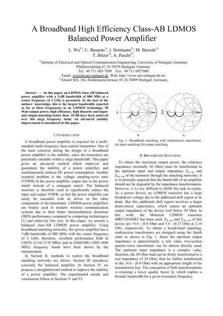
A <strong>Broadband</strong> <strong>High</strong> <strong>Efficiency</strong> <strong>Class</strong>-<strong>AB</strong> <strong>LDMOS</strong><br />
Balanced Power Amplifier<br />
L. Wu 1) , U. Basaran 1) , I. Dettmann 1) , M. Berroth 1)<br />
T. Bitzer 2) , A. Pascht 2) ,<br />
1) Institute of Electrical and Optical Communication Engineering, University of Stuttgart, Germany<br />
Pfaffenwaldring 47, D-70550 Stuttgart, Germany<br />
Tel: 49 711 685-7899 Fax: 49 711 6857900<br />
Email: wu@int.uni-stuttgart.de Web: http://www.uni-stuttgart.de.int<br />
2) Alcatel SEL AG, Holderaeckerstrasse 35, D-70499 Stuttgart, Germany<br />
Abstract — In this paper, an <strong>LDMOS</strong> class-<strong>AB</strong> balanced<br />
power amplifier with a 3-dB bandwidth of 800 MHz at a<br />
center frequency of 2 GHz is presented. To the best of the<br />
authors´ knowledge, this is the largest bandwidth reported<br />
so far at these frequencies in an <strong>LDMOS</strong> technology. 50<br />
Watt output power, high efficiency, high linearity and inputand<br />
output-matching better than -10 dB have been achieved<br />
over this large frequency band. An advanced stability<br />
improvement is introduced in this paper.<br />
I. INTRODUCTION<br />
A broadband power amplifier is required for a multistandard<br />
multi-frequency base-station transmitter. One of<br />
the main concerns during the design of a broadband<br />
power amplifier is the stability, since the transistors are<br />
potentially unstable within a large bandwidth. This paper<br />
gives an advanced method which improves and<br />
guarantees the stability of a power amplifier, and<br />
simultaneously reduces DC power consumption. Another<br />
essential problem is the voltage standing-wave ratio<br />
(VSWR) at the power amplifier output due to the power<br />
match instead of a conjugate match. The balanced<br />
structure is therefore used to significantly reduce the<br />
input and output VSWR, so that the power amplifier can<br />
easily be cascaded with its driver or the other<br />
components in the transmitter. <strong>LDMOS</strong> power amplifiers<br />
are widely used in modern wireless communication<br />
systems due to their better intermodulation distortion<br />
(IMD) performance compared to competing technologies<br />
[1] and relatively low cost. In this paper, we present a<br />
balanced class-<strong>AB</strong> <strong>LDMOS</strong> power amplifier. Using<br />
broadband matching networks, this power amplifier has a<br />
3-dB bandwidth of 800 MHz with the center frequency<br />
of 2 GHz, therefore, excellent performance both in<br />
UMTS (2110-2170 MHz) and in GSM1800 (1805-1880<br />
MHz) frequency bands have been shown by the<br />
measurement.<br />
In Section II, methods to realize the broadband<br />
matching networks are shown. Section III introduces<br />
concisely the balanced amplifier. In Section IV we<br />
propose a straightforward method to improve the stability<br />
of a power amplifier. The experimental results and<br />
conclusions follow in Sections V and VI.<br />
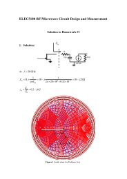
Fig. 1. <strong>Broadband</strong> matching with multisection transformer.<br />
(a) input matching (b) output matching<br />
II. BROADBAND MATCHING<br />
To obtain the maximum output power, the reference<br />
impedance (normally 50 Ohm) must be transformed to<br />
the optimum input and output impedance Z in_opt and<br />
Z out_opt of the transistor through the matching networks. It<br />
is in principle required that the bandwidth of an amplifier<br />
should not be degraded by the impedance transformation.<br />
However, it is very difficult to fulfill this task in reality.<br />
As a power device, an <strong>LDMOS</strong> transistor has a large<br />
breakdown voltage due to the additional drift region at its<br />
drain. But this additional drift region involves a larger<br />
drain-source capacitance, which causes an optimum<br />
output impedance of the device well below 50 Ohm. In<br />
this work, the Motorola <strong>LDMOS</strong> transistor<br />
MRF21030SR3 has been used. Z in_opt and Z out_opt of this<br />
device are 14.6 - j9.4 Ohm and 3.4 - j0.37 Ohm at 2.14<br />
GHz, respectively. To obtain a broad-band matching,<br />
multisection transformers are designed using the Smith<br />
chart as shown in Fig. 1. Since the optimum output<br />
impedance is approximately a real value, two-section<br />
quarter-wave transformer can be almost directly used.<br />
The optimum input impedance is a complex value,<br />
therefore, the 50 Ohm load can be firstly transformed to a<br />
real impedance of 24 Ohm, then be further transformed<br />
to the 14.6 - j9.4 Ohm with an appropriate length of the<br />
transmission line. The conception of both transformations<br />
is retaining a lower quality factor Q, which implies a<br />
broader bandwidth for a given resonance frequency.
Z in_opt<br />
V d<br />
Z out_opt<br />
R<br />
RF-in<br />
input<br />
matching<br />
network<br />
Quadrature<br />
hybrid coupler<br />
V g<br />
A<br />
V d<br />
Output<br />
matching<br />
network<br />
Quadrature<br />
hybrid coupler<br />
50 <br />
(a)<br />
R<br />
(b)<br />
50 <br />
input<br />
matching<br />
network<br />
Z in_opt<br />
B<br />
Z out_opt<br />
Output<br />
matching<br />
network<br />
RF-out<br />
R<br />
R<br />
V g<br />
(c)<br />
(d)<br />
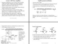
Fig. 2. Balanced power amplifier<br />
Fig. 3. Four types of resistive loading.<br />
III. BALANCED POWER AMPLIFIER<br />
Balanced amplifiers, whose configuration is shown in<br />
Fig. 2, are attractive due to very low VSWR and<br />
excellent cascade-ability. Two identical amplifiers A and<br />
B are connected in parallel through two quadrature<br />
hybrid couplers, which operate as a power divider at the<br />
input and a power combiner at the output, respectively.<br />
Quadrature hybrid couplers are 3-dB directional couplers<br />
with a 90° phase difference in the outputs of the through<br />
and coupled arms. Therefore, at the input of the balanced<br />
amplifier, the two reflected signals from the two<br />
individual amplifiers compensate each other since they<br />
are 180° out of phase, so that the balanced amplifier has<br />
ideally a VSWR of 1 at its input. The same are the two<br />
reflected signals at the output. Therefore, VSWR of a<br />
balanced amplifier depends on the coupler, not on each<br />
individual amplifier. The forward transmitted signals of<br />
the two individual amplifiers are again in phase at the<br />
output, due to the same length of their routes. The S-<br />
parameters of a balanced amplifier can be given as<br />
follows [2]<br />
S11 0.<br />
5 S11A<br />
S11B<br />
(1)<br />
S21 0.<br />
5<br />
S21A<br />
S21B<br />
(2)<br />
S12 0.<br />
5<br />
S12<br />
A<br />
S12B<br />
(3)<br />
S22 0.<br />
5<br />
S22<br />
A<br />
S22B<br />
. (4)<br />
It can be seen that the magnitude of S 11 and S 22 should be<br />
zero, if the two individual amplifiers are absolutely<br />
identical. Excellent stability can therefore be expected<br />
because of the perfect feature of VSWR. In case of entire<br />
identity of two individual amplifiers, the gain of a<br />
balanced power amplifier remains the same as that of a<br />
single amplifier, according to (2). Though the gain of a<br />
balanced power amplifier will not be doubled in spite of<br />
the usage of two devices, the maximum accomplishable<br />
output power of a balanced power amplifier is twice that<br />
of a single amplifier, which is naturally very desired for a<br />
power amplifier design. However, except lots of<br />
advantages, double cost of a balanced power amplifier<br />
due to the usage of two devices is not negligible.<br />
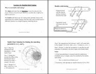
Fig. 4. Stable range (grey range) in Smith charts. (a) without<br />
shunt resistor. (b) with shunt resistor.<br />
V d<br />
Z out_opt<br />
R<br />
Output<br />
matching<br />
network<br />
Fig. 5. Advanced method for stability improvement.<br />
IV. ST<strong>AB</strong>ILITY IMPROVEMENT<br />
50 <br />
Although a balanced amplifier shows an outstanding<br />
stability due to its perfect VSWR, each individual<br />
amplifier of it must also be designed to be stable in its<br />
operating region. Simulations show that MRF21030SR3<br />
is only conditionally stable over a large bandwidth. To<br />
improve the stability, four choices of resistive loading to<br />
the transistor are given in [3]. They are series or shunt<br />
resistor connected at the input or the output of the
transistor as shown in Fig. 3. Resistive loading at the<br />
input is usually not used since it produces a significant<br />
deterioration in the noise performance of the amplifier. A<br />
series resistor at the output is also not so popular since it<br />
can reduce the gain of the amplifier dramatically.<br />
Therefore, suitable shunt resistors R are selected and<br />
separately connected to the drain of each transistor. The<br />
stable ranges in Smith charts simulated at 1.85 GHz<br />
become thereby much larger as illustrated in Fig. 4.<br />
However, the shunt resistors consume large DC power<br />
reducing the power added efficiency (PAE) dramatically.<br />
On the other hand, to ensure the good RF performance of<br />
the power amplifier, resistors of surface mount device<br />
(SMD) should be used, which have only very small<br />
dimensions. However, such devices can be easily<br />
destroyed by a large current resulting in the instability of<br />
the power amplifier again. A new configuration for the<br />
stability improvement is introduced in our work by<br />
adding a series capacitor C to each shunt resistor as<br />
shown in Fig 5. This capacitor prevents a DC current<br />
flowing through the shunt resistor, reduces the total DC<br />
power consumption and protects the resistor R against a<br />
large current. Fig. 6 depicts the simulated current flowing<br />
through each shunt resistor R with or without C, when<br />
the output power is 40 dBm. We remark that the DC part<br />
of the current in (a), which has a magnitude of about 0.52<br />
A, is deleted with the aid of C. Hence, a DC current of<br />
about 1.04 A can be saved for the balanced amplifier.<br />
The series capacitance C must be sufficiently large, in<br />
order to avoid an impedance transformation from the<br />
resistance R selected by stability improvement.<br />
Therefore, the improvement of the stability obtained by<br />
the shunt resistor remains.<br />
current on R, mA<br />
800<br />
700<br />
600<br />
500<br />
400<br />
V. EXPERIMENT<br />
A power amplifier has been fabricated using the<br />
Motorola <strong>LDMOS</strong> transistor MRF21030SR3 as shown in<br />
Fig. 7. The bias voltages are V g = 3.8 V and V d = 26 V. It<br />
has been fabricated on a 0.81 mm-thick RO4003<br />
substrate, which has a relative permittivity of 3.38 and a<br />
conductor thickness of 35 µm. Wilkinson couplers have<br />
been used as power divider and combiner. Because a<br />
Wilkinson divider has two in phase output signals, it is<br />
necessary to shift the phase of the signal before the upper<br />
amplifier and the phase of the signal after the lower<br />
amplifier by 90° using quarter-wave transmission-lines.<br />
Fig. 7. Photograph of the fabricated balanced power<br />
amplifier.<br />
S-parameter, dB<br />
/4-T. L.<br />
20<br />
10<br />
0<br />
-10<br />
-20<br />
S21<br />
-30<br />
S11<br />
S22<br />
-40<br />
1.5 1.7 1.9 2.1 2.3 2.5 2.7<br />
freqency, GHz<br />
/4-T. L.<br />
300<br />
0 200 400 600<br />
800<br />
time, ps<br />
(a)<br />
Fig. 8. Measured magnitudes of the S-parameters.<br />
200<br />
current on R, mA<br />
100<br />
0<br />
-100<br />
-200<br />
0 200 400 600<br />
800<br />
time, ps<br />
(b)<br />
Fig. 6. Simulated current flowing through the shunt resistor R<br />
in the time domain. (a) without C; (b) with C<br />
P out, dBm & PAE, %<br />
P in, dBm<br />
P out at 2.14 GHz<br />
P out at 1.85 GHz<br />
PAE at 2.14 GHz<br />
PAE at 1.85 GHz<br />
gain at 2.14 GHz<br />
gain at 1.85 GHz<br />
Fig. 9. Measured output power, PAE and power gain.<br />
power gain, dB
accomplishes 50 W (47 dBm) at both frequencies. The<br />
1-dB compression points are located at 46 dBm. A PAE<br />
of 35.5% has been achieved at 1.85 GHz for the<br />
maximum output power. At 2.14 GHz, the PAE is as high<br />
as 42.5% for the maximum output power. Even with the<br />
consideration of 6 dB back off from the 1-dB<br />
compression point, a PAE of 20% is obtained at this<br />
frequency. Due to the limited output power of the two<br />
signal generators, the third order intermodulation<br />
distortion versus the output power has been measured<br />
only up to P out = 40 dBm (but just 6 dB back off point in<br />
UMTS band) as shown in Fig. 10. IMD3 better than -<br />
42.5 dBc at 1.85 GHz and than -39 dBc at 2.14 GHz have<br />
been obtained when the output power is lower than 40<br />
dBm.<br />
Fig. 10. Measured third order intermodulation distortion<br />
versus output power.<br />
The 180° out of phase of the two reflected signals at the<br />
input and the output of the balanced amplifier is realized.<br />
The in phase signals at the output of the balanced<br />
amplifier, which are forward transmitted from the two<br />
individual amplifiers can also be obtained in this manner.<br />
Measured S-parameters are shown in Fig. 8. A linear<br />
gain of about 12 dB has been obtained. This power<br />
amplifier has a 3-dB bandwidth of 800 MHz with the<br />
center frequency of 2 GHz, so that it can be adopted<br />
simultaneously both in UMTS and in GSM1800 system.<br />
Magnitudes of S 11 and S 22 of this power amplifier are in<br />
the frequency range of interest between -10 dB and<br />
-30dB. Fig. 9 presents the input-referred output power<br />
P out , PAE and the power gain measured at 1.85 GHz and<br />
2.14 GHz, separately. The maximum output power<br />
VI. CONCLUSION<br />
A 50 W balanced power amplifier using <strong>LDMOS</strong><br />
transistors has been developed. Broad bandwidth, high<br />
efficiency, good linearity and low VSWR prove this<br />
design concept to be a good candidate for multi-standard<br />
multi-frequency base-station transmitters.<br />
REFERENCES<br />
[1] S. R. Novis and L. Pelletier, ‘IMD parameters describe<br />
<strong>LDMOS</strong> device performance’, Microw. RF, vol. 37, pp.<br />
69-74, July 1998.<br />
[2] Guillermo Gonzalez, Microwave transistor amplifiers,<br />
Second edition, pp. 330, Prentice Hall Inc., New Jersey,<br />
1997.<br />
[3] Guillermo Gonzalez, Microwave transistor amplifiers,<br />
Second edition, pp. 225–228, Prentice Hall Inc., New<br />
Jersey, 1997.