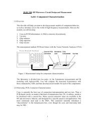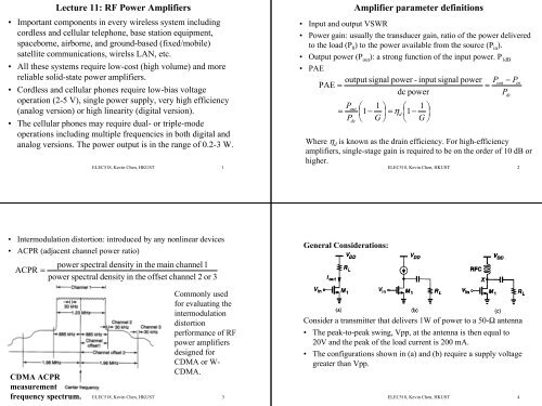
Lecture 11: RF Power Amplifiers Amplifier parameter definitions η
Lecture 11: RF Power Amplifiers Amplifier parameter definitions η
Lecture 11: RF Power Amplifiers Amplifier parameter definitions η

Create successful ePaper yourself
Turn your PDF publications into a flip-book with our unique Google optimized e-Paper software.
<strong>Lecture</strong> <strong>11</strong>: <strong>RF</strong> <strong>Power</strong> <strong><strong>Amplifier</strong>s</strong><br />
• Important components in every wireless system including<br />
cordless and cellular telephone, base station equipment,<br />
spaceborne, airborne, and ground-based (fixed/mobile)<br />
satellite communications, wirelss LAN, etc.<br />
• All these systems require low-cost (high volume) and more<br />
reliable solid-state power amplifiers.<br />
• Cordless and cellular phones require low-bias voltage<br />
operation (2-5 V), single power supply, very high efficiency<br />
(analog version) or high linearity (digital version).<br />
• The cellular phones may require dual- or triple-mode<br />
operations including multiple frequencies in both digital and<br />
analog versions. The power output is in the range of 0.2-3 W.<br />
ELEC518, Kevin Chen, HKUST 1<br />
<strong>Amplifier</strong> <strong>parameter</strong> <strong>definitions</strong><br />
• Input and output VSWR<br />
• <strong>Power</strong> gain: usually the transducer gain, ratio of the power delivered<br />
to the load (P 0 ) to the power available from the source (P in ).<br />
• Output power (P out ): a strong function of the input power. P 1dB<br />
• PAE<br />
output signal power - input signal power Pout<br />
− Pin<br />
PAE =<br />
=<br />
dc power<br />
Pdc<br />
P ⎞ ⎛ ⎞<br />
⎜<br />
⎛ =<br />
out<br />
1 1<br />
1 − ⎟ = ηd<br />
⎜1<br />
− ⎟<br />
P ⎝ G ⎠ ⎝ G ⎠<br />
dc<br />
Where η d is known as the drain efficiency. For high-efficiency<br />
amplifiers, single-stage gain is required to be on the order of 10 dB or<br />
higher.<br />
ELEC518, Kevin Chen, HKUST 2<br />
• Intermodulation distortion: introduced by any nonlinear devices<br />
• ACPR (adjacent channel power ratio)<br />
power spectral density in the main channel 1<br />
ACPR =<br />
power spectral density in the offset channel 2 or 3<br />
General Considerations:<br />
CDMA ACPR<br />
measurement<br />
Commonly used<br />
for evaluating the<br />
intermodulation<br />
distortion<br />
performance of <strong>RF</strong><br />
power amplifiers<br />
designed for<br />
CDMA or W-<br />
CDMA.<br />
Consider a transmitter that delivers 1W of power to a 50-Ω antenna<br />
• The peak-to-peak swing, Vpp, at the antenna is then equal to<br />
20V and the peak of the load current is 200 mA.<br />
• The configurations shown in (a) and (b) require a supply voltage<br />
greater than Vpp.<br />
frequency spectrum. ELEC518, Kevin Chen, HKUST 3<br />
ELEC518, Kevin Chen, HKUST 4
• When a <strong>RF</strong>C is used, the supply voltage can be lowered by a factor of<br />
two because Vx can swing from approximately 0 to 2 V DD .<br />
• The <strong>RF</strong>C approximates a current source that can sustain both positive<br />
and negative voltages.<br />
• The maximum Vds experienced by M1 is not relaxed by the use of the<br />
<strong>RF</strong>C.<br />
• A matching network can be interposed between the PA and the load to<br />
lower supply voltages.<br />
Linear and nonlinear PAs: linearity of Pas becomes important with<br />
certain modulation schemes, e.g., p/4-QPSK<br />
Spectral regrowth and ultimately adjacent channel power.<br />
ELEC518, Kevin Chen, HKUST 5<br />
Nonlinearity is usually characterized by a two -tone test.<br />
ELEC518, Kevin Chen, HKUST 6<br />
• Usually operate with the active device displaying some (maybe<br />
even gross) nonlinear behavior.<br />
• So a big issue for PA design is the nonlinear device modeling<br />
• The major difference between linear <strong>RF</strong> amplifiers design and<br />
PA design is that, for optimum power, the output of the device<br />
(PA) is not presented with the impedance required for a linear<br />
conjugate match.<br />
• In the world of PA design, we often struggle to obtain adequate<br />
signal gain, as well as extract optimum power from a device.<br />
This is an inevitable consequence of cost-driven design; large<br />
periphery transistors have lower gain and designers usually are<br />
constrained to use the lowest cost technology.<br />
Device Models: Linear and Nonlinear<br />
• An essential part of CAD tools<br />
• Reduced design cycle time and possible “first-pass” design<br />
• Most common method of model development is to measure DC<br />
and S-<strong>parameter</strong>s.<br />
• Model extractions are carried out to replicate the measured S-<br />
<strong>parameter</strong>s<br />
ELEC518, Kevin Chen, HKUST 7<br />
ELEC518, Kevin Chen, HKUST 8
Linear Device Model<br />
Typical small-signal model <strong>parameter</strong>s for 300-mm power FET<br />
biased at Vds = 2.5 V, Ids = 50% Idss<br />
Equivalent Circuit of an<br />
<strong>RF</strong>/microwave transistor<br />
• Cgs, Cgd, g m and Rds are a strong function of device bias<br />
conditions.<br />
• At given bias, this model describes basic linear operation of a<br />
FET and the model reproduces the small-signal <strong>RF</strong> terminal<br />
characteristics of the device with good accuracy.<br />
ELEC518, Kevin Chen, HKUST 9<br />
ELEC518, Kevin Chen, HKUST 10<br />
Disadvantages of the Equivalent-Circuit<br />
Model<br />
• Difficult to scale to physical structures<br />
• Frequency independent of circuit elements<br />
• No time dependence feature<br />
• Incoherent limitation to linear circuits<br />
ELEC518, Kevin Chen, HKUST <strong>11</strong><br />
Nonlinear Device Models for CAD<br />
• The PA designer is much more sensitive to some of the<br />
shortcomings of widely used CAD models than designers of many<br />
other kinds of <strong>RF</strong> devices.<br />
• So a big issue for PA design is the nonlinear device modeling<br />
• Device models for CAD fall into two categories: physical models<br />
(bottom up); curve-fit, or top-down approach.<br />
• Interesting to note: bipolar modeling community has, historically,<br />
stuck rigidly to the physical model path, while the available FET<br />
models are largely of the top-down type.<br />
• Central issue in modeling an <strong>RF</strong> power transistor: scaling<br />
• Almost always, the detailed modeling and curve fitting are done on a<br />
small periphery sample device and may be quite accurate.<br />
ELEC518, Kevin Chen, HKUST 12
• The PA designer has to take the small cell and scale it by tens,<br />
even hundreds, to “build” a power transistor.<br />
• Such a scaling, unfortunately, is not a simple set of electrical nodal<br />
connections.<br />
• Secondary phenomena associated with large periphery devices:<br />
– Nonuniform thermal effects --- against the customary assumptions made<br />
about equal currents and voltages across an array of “identical” circuit<br />
elements.<br />
– Multiple parallel connections also can cause mutual coupling between<br />
bondwires.<br />
• The most difficult part of the scale-up <strong>RF</strong> power transistor models<br />
is the difficulty of putting the model and the device through simple<br />
comparative tests.<br />
– DC I-V curves: curve tracers are too slow for <strong>RF</strong> power transistors. The<br />
measured I-V characteristics usually include the transient junction heating<br />
effects, which will not occur to any significant extent during an <strong>RF</strong> cycle.<br />
ELEC518, Kevin Chen, HKUST 13<br />
– Pulsed I-V measurement is attracting increasing interests, but<br />
the measurement system is expensive --- usually provide I-V<br />
data quite different from that obtained using curve tracers ---<br />
results in “dispersion”<br />
– The impedances are typically so low, compared to a 50Ω<br />
reference, that even simple linear s-<strong>parameter</strong> measurement is<br />
fraught with calibration problems --- pre-matching --- additional<br />
challenging calibration problems in de-embedding the matching<br />
networks.<br />
ELEC518, Kevin Chen, HKUST 14<br />
Nonlinear model<br />
• Using the same basic configuration for equivalent circuit.<br />
Measurement-based.<br />
• Various models differ in the expressions for the drain current, gatesource<br />
and gate-drain capacitances.<br />
• Commonly used representation of the nonlinear FET model<br />
2 3<br />
I = ( A + AV + A V + AV ) tanh( αV<br />
)<br />
where<br />
and<br />
ds<br />
0 1 1 2 1 3 1<br />
ds<br />
V = V [1 + β ( V<br />
−V<br />
1 gs<br />
dso ds<br />
C<br />
C<br />
gs<br />
gd<br />
= C<br />
= C<br />
gso<br />
gdo<br />
⋅ f ( Vgs,<br />
Vgd<br />
)<br />
⋅ f V , V )<br />
(<br />
gs gd<br />
)]<br />
Basic steps in nonlinear equivalent Circuit<br />
model extraction<br />
• Extract coefficients for I ds to match with measured I-V data.<br />
Important data is near the knee of the curves and breakdown near<br />
pinchoff.<br />
• Measure S-<strong>parameter</strong>s, extract small-signal model values and<br />
derive coefficients for gate-source and gate-drain capacitances to<br />
describe its dependence on gate and drain voltages.<br />
• Validate model by comparing measured and simulated data with<br />
50 ohm input and output for P 1dB compression point and power<br />
levels for other harmonics. Simulations are generally carried out<br />
using harmonic balance analysis.<br />
ELEC518, Kevin Chen, HKUST 15<br />
ELEC518, Kevin Chen, HKUST 16
Summary on Nonlinear Device Modeling<br />
• Equivalent circuit models can be easily integrated into circuit<br />
simulators.<br />
• Satisfactory to good for a well-designed circuit, especially for<br />
mildly nonlinear applications such as class A power amplifiers not<br />
operating in hard saturation.<br />
• Biggest problem: scaling in frequency and bias<br />
• Neglect of domain capacitance and the interdependence of the<br />
nonlinear elements, e.g., g m and gate-source capacitance.<br />
• Any change in device <strong>parameter</strong>s needs another round of modeling<br />
extraction and validation.<br />
ELEC518, Kevin Chen, HKUST 17<br />
High-Efficiency <strong>Amplifier</strong> Modes<br />
• A mobile phone handset PA has to be as efficient as possible to<br />
conserve battery power (increase talk time)<br />
• Base stations also have efficiency specifications due to power<br />
cooling limitations.<br />
Definition of conduction angle<br />
The portion of the <strong>RF</strong> cycle for<br />
which conduction occurs.<br />
V t : threshold voltage, or cutoff<br />
voltage<br />
V q : normalized quiescent bias point,<br />
defined according to V t = 0, V 0 = 1.<br />
The required signal voltage<br />
amplitude: Vs = 1- V q<br />
ELEC518, Kevin Chen, HKUST 18<br />
Classification of <strong>Power</strong> <strong><strong>Amplifier</strong>s</strong>: A, AB, B, C<br />
Fourier analysis of reduced<br />
conduction angle mode<br />
max<br />
2sin( α / 2) −α<br />
cos( α / 2)<br />
= I<br />
2π<br />
1−<br />
cos( α / 2)<br />
• The DC component of the output current will decrease as the<br />
conduction angle is reduced.<br />
• The variation of the fundamental and other harmonics as a<br />
function of the conduction angle can be found by Fourier analysis<br />
of the waveforms.<br />
I dc<br />
max<br />
α − sinα<br />
I1<br />
= I<br />
2π<br />
1−<br />
cos( α / 2)<br />
• DC component decreases<br />
monotonically as the<br />
conduction angle is reduced.<br />
• For the class B condition,<br />
α = π, gives<br />
I dc<br />
( class B) = I<br />
max<br />
/π<br />
• Class A gives<br />
I dc<br />
( class A) = I<br />
max<br />
/ 2<br />
ELEC518, Kevin Chen, HKUST 19<br />
ELEC518, Kevin Chen, HKUST 20
• For the class B condition,<br />
α = π, gives the<br />
fundamental component as<br />
I<br />
1( class B) = I<br />
max<br />
/ 2<br />
The same as the fundamental<br />
component in the class A condition<br />
Hint: there appears to be a possibility for decreasing the dc supply<br />
power by a factor of π/2, without changing the <strong>RF</strong> fundamental<br />
component. In other words, the efficiency should increase from 1/2 in<br />
the class A mode to π/4 (about 78.5%) in class B.<br />
To realize the possible higher efficiency, the output termination and<br />
voltage waveform have to be considered first.<br />
• The odd harmonics pass through zero at the class B point, but in<br />
AB mode, the third harmonic is not negligible.<br />
ELEC518, Kevin Chen, HKUST 21<br />
Circuit analysis for output<br />
termination<br />
Conceptually, all harmonics of<br />
the load are shorted and generate<br />
no voltage.<br />
The harmonic short is realized<br />
conceptually with a high-Q<br />
parallel resonant “tank” circuit<br />
at the fundamental.<br />
The <strong>RF</strong> fundamental output<br />
power is given by<br />
Vdc<br />
I1<br />
P1<br />
=<br />
2 2<br />
ELEC518, Kevin Chen, HKUST 22<br />
The dc supply power is given by<br />
P = V<br />
The output efficiency is defined by: P η = 1<br />
P dc<br />
In an <strong>RF</strong> PA, the <strong>RF</strong> driver power (input) is quite substantial, which<br />
leads to an alternative definition, the so-called power added-efficiency<br />
(PAE): P − PIN<br />
PAE = 1<br />
P<br />
<strong>RF</strong> power and efficiency as a<br />
function of conduction angle<br />
dc<br />
Optimum load and<br />
harmonic short assumed<br />
dc<br />
dc<br />
ELEC518, Kevin Chen, HKUST 23<br />
I<br />
dc<br />
Summary of class A, AB, B, and C PAs<br />
• Between class A and class B operation, the fundamental <strong>RF</strong> output<br />
power is approximately constant, showing an increase of a few<br />
tenths of a decibel in the mid-AB range over the class A power<br />
output.<br />
• The class B delivers the same power as class A but with a dc supply<br />
reduced by a factor of π/2 compared to class A, giving an ideal<br />
efficiency of π /4.<br />
• The class C condition shows a rapidly increasing efficiency as the<br />
conduction angle is reduced to low values; however, that efficiency<br />
is accompanied by a substantial reduction in <strong>RF</strong> output power.<br />
Reduced conduction angle mode analysis: a simple program that<br />
computes the necessary Fourier components of the <strong>RF</strong> current<br />
waveforms for a given set of conditions that specify the bias<br />
quiescent point and the amplitude of the <strong>RF</strong> drive signal.<br />
ELEC518, Kevin Chen, HKUST 24
Class A operation<br />
The dotted traces show 3 dB backed-off<br />
condition.<br />
Required <strong>parameter</strong>s:<br />
Vq<br />
= 0.5; Vs<br />
= 0.5<br />
V = 0; R = 1.0<br />
ELEC518, Kevin Chen, HKUST 25<br />
k<br />
V k is a normalized<br />
<strong>parameter</strong> that allows<br />
a more realistic turnon<br />
(“knee”) transistor<br />
characteristics to be<br />
included in the<br />
analysis. Set to be<br />
zero here.<br />
R L : normalized value of<br />
fundamental load<br />
resistance, normalized to<br />
the optimum class A value<br />
of unity.<br />
L<br />
Class AB operation<br />
If the linear gain starts off below 10 dB,<br />
the PAE will start to show a markedly<br />
less attractive increase in overall<br />
efficiency.<br />
Required <strong>parameter</strong>s:<br />
V<br />
V<br />
q<br />
k<br />
= 0.25; V<br />
= 0;<br />
= 0.75<br />
= 0.94<br />
ELEC518, Kevin Chen, HKUST 26<br />
R<br />
L<br />
R L is reduced from the class<br />
A loadline value, reflecting<br />
the higher fundamental<br />
current component.<br />
Efficiency now increases to<br />
70%, which comes at the<br />
expense of drive power: the<br />
increase in Vs from 0.5 to<br />
0.75 translates ideally into<br />
about 3.5 dB extra drive<br />
power.<br />
s<br />
Class B operation<br />
Use hotter technology (such as GaAs<br />
HBT and PHEMT) for cellular phone<br />
handsets below 2 GHz, so that we have a<br />
higher gain starting point.<br />
Required <strong>parameter</strong>s:<br />
Vq<br />
= 0; Vs<br />
= 1.0<br />
V = 0; R = 1.0<br />
k<br />
ELEC518, Kevin Chen, HKUST 27<br />
L<br />
The <strong>RF</strong> power has returned<br />
to its original (class A)<br />
value. The dc supply is<br />
down by a factor of π/2 and<br />
the efficiency has increased<br />
to 78.5%.<br />
The downside is that, in<br />
theory, 6 dB more drive<br />
power is needed --- a large<br />
reduction in power gain at<br />
<strong>RF</strong> and microwave<br />
frequencies.<br />
Class C operation<br />
The major problem with using class C<br />
mode in solid state applications is the<br />
large negative swing of input voltage ---<br />
reverse breakdown involved.<br />
Required <strong>parameter</strong>s:<br />
V<br />
V<br />
q<br />
k<br />
= −0.5;<br />
V<br />
= 0;<br />
= 1.5<br />
= 1.14<br />
ELEC518, Kevin Chen, HKUST 28<br />
R<br />
L<br />
The current waveform is<br />
reduced to a train of short<br />
pulses, which have low dc<br />
component but also a lower<br />
fundamental <strong>RF</strong><br />
component. Very high<br />
efficiency can be obtained,<br />
but at the expense of lower<br />
<strong>RF</strong> output power and very<br />
heavy input drive<br />
requirements.<br />
s
Switch Mode PAs<br />
Class E: nonlinear PAs that achieve efficiencies approaching 100%<br />
while delivering full power, while delivering full power, a<br />
remarkable advantage over class C PAs.<br />
• The transistor operates as a switch,<br />
rather than a voltage-dependent current<br />
source.<br />
• Requirement for achieving high<br />
efficiency<br />
– M1 sustains a small voltage when it carries<br />
current<br />
– M1 carries a small current when it sustains a<br />
finite voltage<br />
– inevitable transition times between on and<br />
off states are minimized.<br />
Class E PAs deal with finite input and output transition times by<br />
proper load design.<br />
The components in the load are chosen so that Vx satisfies three<br />
conditions:<br />
(1) As the switch turns off, Vx remains low long enough for the<br />
current to drop to zero, (2) Vx reaches zero just before the switch<br />
turns on, and (3) dVx/dt is also near zero when the switch turns on.<br />
underdamped<br />
critically damped<br />
overdamped<br />
ELEC518, Kevin Chen, HKUST 29<br />
ELEC518, Kevin Chen, HKUST 30<br />
Class E stages exhibit trade-off between efficiency and output<br />
harmonic content. Additional filtering can precede the load resistor,<br />
but at the cost of power loss in the filter.<br />
Large peak voltage is required for class E PAs. Usually drain-source<br />
has to endure three times of the V DD .<br />
ELEC518, Kevin Chen, HKUST 31<br />
Large-Signal Impedance Matching: load-pull<br />
measurement<br />
Commercial load-pull equipment<br />
Both mechanical<br />
and electronic<br />
tuners have been<br />
used in<br />
commercial loadpull<br />
systems.<br />
Systems with<br />
independent<br />
fundamental and<br />
harmonic tuning<br />
are also available.<br />
Typical load-pull configuration<br />
ELEC518, Kevin Chen, HKUST 32
Typical load-pull measurement results<br />
ELEC518, Kevin Chen, HKUST 33