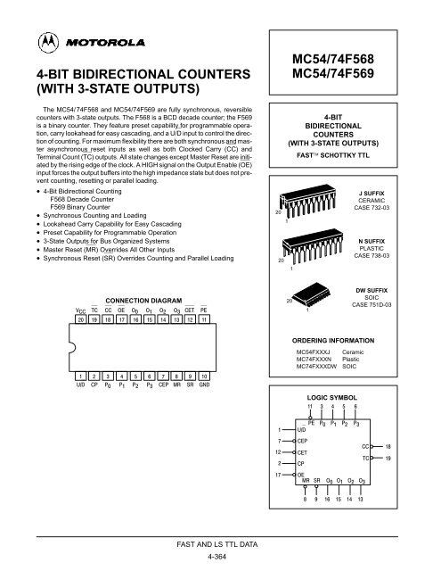
4-BIT BIDIRECTIONAL COUNTERS (WITH 3-STATE ... - skot9000
4-BIT BIDIRECTIONAL COUNTERS (WITH 3-STATE ... - skot9000
4-BIT BIDIRECTIONAL COUNTERS (WITH 3-STATE ... - skot9000

You also want an ePaper? Increase the reach of your titles
YUMPU automatically turns print PDFs into web optimized ePapers that Google loves.
4-<strong>BIT</strong> <strong>BIDIRECTIONAL</strong> <strong>COUNTERS</strong><br />
(<strong>WITH</strong> 3-<strong>STATE</strong> OUTPUTS)<br />
The MC54/74F568 and MC54/74F569 are fully synchronous, reversible<br />
counters with 3-state outputs. The F568 is a BCD decade counter; the F569<br />
is a binary counter. They feature preset capability for programmable operation,<br />
carry lookahead for easy cascading, and a U/D input to control the direction<br />
of counting. For maximum flexibility there are both synchronous and master<br />
asynchronous reset inputs as well as both Clocked Carry (CC) and<br />
Terminal Count (TC) outputs. All state changes except Master Reset are initiated<br />
by the rising edge of the clock. A HIGH signal on the Output Enable (OE)<br />
input forces the output buffers into the high impedance state but does not prevent<br />
counting, resetting or parallel loading.<br />
• 4-Bit Bidirectional Counting<br />
F568 Decade Counter<br />
F569 Binary Counter<br />
• Synchronous Counting and Loading<br />
• Lookahead Carry Capability for Easy Cascading<br />
• Preset Capability for Programmable Operation<br />
• 3-State Outputs for Bus Organized Systems<br />
• Master Reset (MR) Overrides All Other Inputs<br />
• Synchronous Reset (SR) Overrides Counting and Parallel Loading<br />
20<br />
20<br />
1<br />
MC54/74F568<br />
MC54/74F569<br />
4-<strong>BIT</strong><br />
<strong>BIDIRECTIONAL</strong><br />
<strong>COUNTERS</strong><br />
(<strong>WITH</strong> 3-<strong>STATE</strong> OUTPUTS)<br />
1<br />
FAST SCHOTTKY TTL<br />
J SUFFIX<br />
CERAMIC<br />
CASE 732-03<br />
N SUFFIX<br />
PLASTIC<br />
CASE 738-03<br />
<br />
CONNECTION DIAGRAM<br />
<br />
<br />
<br />
<br />
20<br />
1<br />
DW SUFFIX<br />
SOIC<br />
CASE 751D-03<br />
<br />
<br />
<br />
<br />
<br />
ORDERING INFORMATION<br />
MC54FXXXJ<br />
MC74FXXXN<br />
MC74FXXXDW<br />
Ceramic<br />
Plastic<br />
SOIC<br />
<br />
<br />
<br />
<br />
<br />
<br />
<br />
<br />
LOGIC SYMBOL<br />
<br />
<br />
<br />
<br />
<br />
<br />
<br />
<br />
<br />
<br />
<br />
<br />
<br />
<br />
<br />
<br />
<br />
<br />
<br />
FAST AND LS TTL DATA<br />
4-364
MC54/74F568 • MC54/74F569<br />
Symbol Parameter Min Typ Max Unit<br />
VCC Supply Voltage 54, 74 4.5 5.0 5.5 V<br />
TA<br />
Operating Ambient Temperature Range<br />
54 –55 25 125<br />
74 0 25 70<br />
°C<br />
IOH Output Current — High 54, 74 –3.0 mA<br />
IOL Output Current — Low 54, 74 24 mA<br />
FUNCTIONAL DESCRIPTION<br />
The F568 counts modulo-10 in the BCD (8421) sequence.<br />
From state 9 (HLLH) it will increment to 0 (LLLL) in the Up<br />
mode; in Down mode it will decrement from 0 to 9.The F569<br />
counts in the modulo-16 binary sequence. From state 15 it will<br />
increment to state 0 in the Up mode; in the Down mode it will<br />
decrement from 0 to 15. The clock inputs of all flip-flops are<br />
driven in parallel through a clock buffer. All state changes (except<br />
due to Master Reset) occur synchronously with the LOWto-HIGH<br />
transition of the Clock Pulse (CP) input signal.<br />
The circuits have five fundamental modes of operation, in<br />
order of precedence: asynchronous reset, synchronous reset,<br />
parallel load, count and hold. Five control inputs — Master Reset<br />
(MR), Synchronous Reset (SR), Parallel Enable (PE),<br />
Count Enable Parallel (CEP) and Count Enable Trickle (CET)<br />
— plus the Up/Down (U/D) input, determine the mode of operation,<br />
as shown in the Mode Select Table. A LOW signal on<br />
MR overrides all other inputs and asynchronously forces the<br />
flip-flop Q outputs LOW. A LOW signal on SR overrides counting<br />
and parallel loading and allows the Q outputs to go LOW<br />
on the next rising edge of CP. A LOW signal on PE overrides<br />
counting and allows information on the Parallel Data (Pn) inputs<br />
to be loaded into the flip-flops on the next rising edge of<br />
CP. With MR, SR and PE HIGH, CEP and CET permit counting<br />
when both are LOW. Conversely, a HIGH signal on either CEP<br />
or CET inhibits counting.<br />
The F568 and F569 use edge-triggered flip-flops and<br />
changing the SR, PE, CEP , CET or U/D inputs when the CP<br />
is in either state does not cause errors, provided that the recommended<br />
setup and hold times, with respect to the rising<br />
edge of CP, are observed.<br />
Two types of outputs are provided as overflow/underflow indicators.<br />
The Terminal Count (TC) output is normally HIGH<br />
and goes LOW providing CET is LOW, when the counter<br />
reaches zero in the Down mode, or reaches maximum (9 for<br />
the F568,15 for the F569) in the Up mode. TC will then remain<br />
LOW until a state change occurs, whether by counting or presetting,<br />
or until U/D or CET is changed. To implement synchronous<br />
multistage counters, the connections between the TC<br />
output and the CEP and CET inputs can provide either slow<br />
or fast carry propagation. Figure A shows the connections for<br />
simple ripple carry, in which the clock period must be longer<br />
than the CP to TC delay of the first stage, plus the cumulative<br />
CET to TC delays of the intermediate stages, plus the CET to<br />
CP setup time of the last stage. This total delay plus setup time<br />
sets the upper limit on clock frequency. For faster clock rates,<br />
the carry lookahead connections shown in Figure B are recommended.<br />
In this scheme the ripple delay through the intermediate<br />
stages commences with the same clock that causes<br />
the first stage to tick over from max to min in the Up mode, or<br />
min to max in the Down mode, to start its final cycle. Since this<br />
final cycle takes 10 (F568) or 16 (F569) clocks to complete,<br />
there is plenty of time for the ripple to progress through the intermediate<br />
stages. The critical timing that limits the clock period<br />
is the CP to TC delay of the first stage plus the CEP to CP<br />
setup time of the last stage. The TC output is subject to decoding<br />
spikes due to internal race conditions and is therefore not<br />
recommended for use as a clock or asynchronous reset for<br />
flip-flops, registers or counters. For such applications, the<br />
Clocked Carry (CC) output is provided. The CC output is normally<br />
HIGH. When CEP, CET, and TC are LOW, the CC output<br />
will go LOW when the clock next goes LOW and will stay LOW<br />
until the clock goes HIGH again, as shown in the CC Truth<br />
Table. When the Output Enable (OE) is LOW, the parallel data<br />
outputs O0–O3 are active and follow the flip-flop Q outputs. A<br />
HIGH signal on OE forces O0–O3 to the High Z state but does<br />
not prevent counting, loading or resetting.<br />
LOGIC EQUATIONS:<br />
Count Enable = CEP⋅CET⋅PE<br />
Up (’F568): TC = Q0⋅Q1⋅Q2⋅Q3⋅(Up)⋅CET<br />
(’F569): TC = Q0⋅Q1⋅Q2⋅Q3⋅(Up)⋅CET<br />
Down (Both): TC = Q0⋅Q1⋅Q2⋅Q3⋅(Down)⋅CET<br />
CC TRUTH TABLE<br />
Inputs<br />
Output<br />
SR PE CEP CET TC* CP CC<br />
L X X X X X H<br />
X L X X X X H<br />
X X H X X X H<br />
X X X H X X H<br />
X X X X H X H<br />
H H L L L<br />
* = TC is generated internally X = Don’t Care<br />
L = LOW Voltage Level<br />
= Low Pulse<br />
H = HIGH Voltage Level<br />
FUNCTION TABLE<br />
Inputs<br />
MR SR PE CEP CET U/D CP<br />
Operating Mode<br />
L X X X X X X Asynchronous reset<br />
h l X X X X ↑ Synchronous reset<br />
h h l X X X ↑ Parallel load<br />
h h h l l h ↑<br />
h h h l l l ↑<br />
h H H H X X X<br />
h H H X H X X<br />
Count up<br />
(increment)<br />
Count down<br />
(decrement)<br />
Hold (do nothing)<br />
H = HIGH voltage level<br />
h = HIGH voltage level one setup prior to the Low-to-High Clock transition<br />
L = LOW voltage level<br />
l = LOW voltage level one setup prior to the Low-to-High clock transition<br />
X = Don’t care<br />
↑ = Low-to-High clock transition<br />
FAST AND LS TTL DATA<br />
4-365
MC54/74F568 • MC54/74F569<br />
<br />
<br />
<br />
LOGIC DIAGRAMS<br />
MC54/74F568<br />
<br />
<br />
<br />
<br />
<br />
<br />
<br />
<br />
<br />
<br />
<br />
<br />
<br />
<br />
<br />
<br />
<br />
<br />
<br />
<br />
<br />
<br />
<br />
<br />
<br />
<br />
<br />
<br />
<br />
<br />
<br />
<br />
<br />
<br />
<br />
<br />
<br />
<br />
<br />
<br />
<br />
<br />
MC54/74F569<br />
<br />
<br />
<br />
<br />
<br />
<br />
<br />
<br />
<br />
<br />
<br />
<br />
<br />
<br />
<br />
<br />
<br />
<br />
<br />
<br />
<br />
<br />
<br />
<br />
<br />
<br />
<br />
<br />
<br />
<br />
<br />
<br />
<br />
<br />
<br />
<br />
<br />
<br />
Please note that these diagrams are provided only for the understanding of logic<br />
operations and should not be used to estimate propagation delays.<br />
<br />
FAST AND LS TTL DATA<br />
4-366
MC54/74F568 • MC54/74F569<br />
Figure A. Multistage Counter with Ripple Carry<br />
<br />
<br />
<br />
<br />
<br />
<br />
Figure B. Multistage Counter with Lookahead Carry<br />
<br />
<br />
<br />
<br />
<br />
<br />
<br />
<br />
<br />
<br />
<br />
<br />
<br />
<br />
<br />
<br />
<br />
<br />
DC CHARACTERISTICS OVER OPERATING TEMPERATURE RANGE (unless otherwise specified)<br />
Symbol<br />
Parameter<br />
Limits<br />
Min Typ Max<br />
VIH Input HIGH Voltage 2.0 V<br />
Unit<br />
Test Conditions<br />
Guaranteed Input HIGH Voltage for<br />
All Inputs<br />
VIL Input LOW Voltage 0.8 V<br />
Guaranteed Input LOW Voltage for<br />
All Inputs<br />
VIK Input Clamp Diode Voltage –1.2 V VCC = MIN, IIN = –18 mA<br />
VOH<br />
Output HIGH Voltage<br />
54, 74 2.4 3.3 V IOH = –3.0 mA VCC = 4.5 V<br />
74 2.7 3.3 V IOH = –3.0 mA VCC = 4.75 V<br />
VOL Output LOW Voltage 0.3 0.5 V IOL = 24 mA VCC = MIN<br />
IOZH Output OFF Current — HIGH 50 µA VOUT = 2.7 V VCC = MAX<br />
IOZL Output OFF Current — LOW –50 µA VOUT = 0.5 V VCC = MAX<br />
IIH<br />
IIL<br />
Input HIGH Current<br />
Input LOW Current<br />
PE, CET<br />
Others<br />
20<br />
100<br />
–1.2<br />
–0.6<br />
µA<br />
mA<br />
VIN = 2.7 V<br />
VIN = 7.0 V<br />
VCC = MAX, VIN = 0.5 V<br />
VCC = MAX<br />
IOS Output Short Circuit Current (Note 2) –60 –150 mA VOUT = 0 V VCC = MAX<br />
ICC<br />
Power Supply Current<br />
(ALL Outputs OFF)<br />
67 mA VCC = MAX<br />
NOTES:<br />
1. For conditions such as MIN or MAX, use the appropriate value specified under recommended operating conditions for the applicable device type.<br />
2. Not more than one output should be shorted at a time, nor for more than 1 second.<br />
FAST AND LS TTL DATA<br />
4-367
MC54/74F568 • MC54/74F569<br />
<strong>STATE</strong> DIAGRAMS<br />
MC54/74F568<br />
MC54/74F569<br />
<br />
<br />
<br />
<br />
<br />
<br />
<br />
<br />
<br />
<br />
<br />
<br />
<br />
<br />
<br />
<br />
<br />
<br />
<br />
<br />
<br />
<br />
<br />
<br />
<br />
<br />
<br />
<br />
<br />
AC CHARACTERISTICS<br />
54/74F 54F 74F<br />
TA = +25°C<br />
VCC = +5.0 V<br />
CL = 50 pF<br />
TA = –55 to +125°C<br />
VCC = 5.0 V ±10%<br />
CL = 50 pF<br />
TA = 0 to +70°C<br />
VCC = 5.0 V ±10%<br />
CL = 50 pF<br />
Symbol Parameter Min Max Min Max Min Max Unit<br />
fmax Maximum Clock Frequency 100 60 85 MHz<br />
tPLH<br />
tPHL<br />
Propagation Delay<br />
CP to On (PE HIGH or LOW)<br />
3.0<br />
4.0<br />
8.5<br />
11.5<br />
3.0<br />
4.0<br />
10.5<br />
14<br />
3.0<br />
4.0<br />
9.5<br />
13<br />
ns<br />
tPLH<br />
tPHL<br />
Propagation Delay<br />
CP to TC<br />
5.5<br />
4.0<br />
15.5<br />
11<br />
5.5<br />
4.0<br />
18.5<br />
13.5<br />
5.5<br />
4.0<br />
17.5<br />
12.5<br />
ns<br />
tPLH<br />
tPHL<br />
Propagation Delay<br />
CET to TC<br />
2.5<br />
2.5<br />
6.0<br />
8.0<br />
2.5<br />
2.5<br />
8.0<br />
10<br />
2.5<br />
2.5<br />
7.0<br />
9.0<br />
ns<br />
tPLH<br />
tPHL<br />
Propagation Delay<br />
U/D to TC (′F568)<br />
3.5<br />
4.0<br />
11<br />
16<br />
3.5<br />
4.0<br />
13.5<br />
19<br />
3.5<br />
4.0<br />
12.5<br />
18<br />
ns<br />
tPLH<br />
tPHL<br />
Propagation Delay<br />
U/D to TC (′F569)<br />
3.5<br />
4.0<br />
11<br />
10.5<br />
3.5<br />
4.0<br />
13.5<br />
13<br />
3.5<br />
4.0<br />
12.5<br />
12<br />
ns<br />
tPLH<br />
tPHL<br />
Propagation Delay<br />
CP to CC<br />
2.5<br />
2.0<br />
7.0<br />
6.0<br />
2.5<br />
2.0<br />
9.0<br />
8.0<br />
2.5<br />
2.0<br />
8.0<br />
7.0<br />
ns<br />
tPLH<br />
tPHL<br />
Propagation Delay<br />
CEP, CET to CC<br />
2.5<br />
4.0<br />
6.5<br />
11<br />
2.5<br />
4.0<br />
8.5<br />
13.5<br />
2.5<br />
4.0<br />
7.5<br />
12.5<br />
ns<br />
tPHL<br />
Propagation Delay<br />
MR to On<br />
5.0 13 5.0 15.5 5.0 14.5 ns<br />
tPZH<br />
tPZL<br />
Output Enable Time<br />
OE to On<br />
2.5<br />
3.0<br />
7.0<br />
8.0<br />
2.5<br />
3.0<br />
9.0<br />
10<br />
2.5<br />
3.0<br />
8.0<br />
9.0<br />
ns<br />
tPHZ<br />
tPLZ<br />
Output Disable Time<br />
OE to On<br />
1.5<br />
2.0<br />
6.5<br />
6.0<br />
1.5<br />
2.0<br />
8.5<br />
8.0<br />
1.5<br />
2.0<br />
7.5<br />
7.0<br />
ns<br />
FAST AND LS TTL DATA<br />
4-368
MC54/74F568 • MC54/74F569<br />
AC OPERATING REQUIREMENTS<br />
54/74F 54F 74F<br />
TA = +25°C<br />
VCC = +5.0 V<br />
TA = –55°C to +125°C<br />
VCC = 5.0 V ±10%<br />
TA = 0°C to +70°C<br />
VCC = 5.0 V ±10%<br />
Symbol Parameter Min Max Min Max Min Max Unit<br />
ts(H)<br />
ts(L)<br />
th(H)<br />
th(L)<br />
Setup Time, HIGH or LOW<br />
Pn to CP<br />
Hold Time, HIGH or LOW<br />
Pn to CP<br />
4.0<br />
4.0<br />
3.0<br />
3.0<br />
5.5<br />
5.5<br />
3.5<br />
3.5<br />
4.5<br />
4.5<br />
3.5<br />
3.5<br />
ns<br />
ts(H)<br />
ts(L)<br />
th(H)<br />
th(L)<br />
Setup Time, HIGH or LOW<br />
CEP or CET to CP<br />
Hold Time, HIGH or LOW<br />
CEP or CET to CP<br />
5.0<br />
5.0<br />
0<br />
0<br />
7.0<br />
7.0<br />
0<br />
0<br />
6.0<br />
6.0<br />
0<br />
0<br />
ns<br />
ts(H)<br />
ts(L)<br />
th(H)<br />
th(L)<br />
Setup Time, HIGH or LOW<br />
PE to CP<br />
Hold Time, HIGH or LOW<br />
PE to CP<br />
8.0<br />
8.0<br />
0<br />
0<br />
10<br />
10<br />
0<br />
0<br />
9.0<br />
9.0<br />
0<br />
0<br />
ns<br />
ts(H)<br />
ts(L)<br />
Setup Time, HIGH or LOW<br />
U/D to CP (F568)<br />
11<br />
16.5<br />
13.5<br />
18.5<br />
12.5<br />
17.5<br />
ns<br />
ts(H)<br />
ts(L)<br />
Setup Time, HIGH or LOW<br />
U/D to CP (F569)<br />
11<br />
7.0<br />
13.5<br />
10<br />
12.5<br />
8.0<br />
ns<br />
th(H)<br />
th(L)<br />
Hold Time, HIGH or LOW<br />
U/D to CP<br />
0<br />
0<br />
0<br />
0<br />
0<br />
0<br />
ns<br />
ts(H)<br />
ts(L)<br />
th(H)<br />
th(L)<br />
Setup Time, HIGH or LOW<br />
SR to CP<br />
Hold Time, HIGH or LOW<br />
SR to CP<br />
10<br />
8.0<br />
0<br />
0<br />
12<br />
10.5<br />
0<br />
0<br />
11<br />
9.5<br />
0<br />
0<br />
ns<br />
tw(H)<br />
tw(L)<br />
CP Pulse Width HIGH or LOW<br />
4.0<br />
6.0<br />
6.0<br />
8.0<br />
4.5<br />
6.5<br />
ns<br />
tw(L) MR Pulse Width, LOW 4.5 6.0 5.0 ns<br />
trec MR Recovery Time 6.0 8.0 7.0 ns<br />
FAST AND LS TTL DATA<br />
4-369
20<br />
-A-<br />
11<br />
1 10<br />
-B-<br />
P<br />
<br />
Case 751D-03 DW Suffix<br />
20-Pin Plastic<br />
SO-20 (WIDE)<br />
<br />
<br />
<br />
<br />
<br />
<br />
<br />
<br />
<br />
<br />
<br />
<br />
<br />
-T-<br />
G<br />
D <br />
<br />
C<br />
K<br />
<br />
<br />
R X 45°<br />
M F J<br />
<br />
<br />
<br />
<br />
<br />
<br />
<br />
<br />
<br />
<br />
<br />
<br />
<br />
<br />
<br />
<br />
<br />
<br />
<br />
<br />
<br />
°<br />
<br />
<br />
<br />
<br />
<br />
<br />
<br />
<br />
<br />
<br />
°<br />
<br />
<br />
<br />
<br />
<br />
<br />
<br />
<br />
<br />
<br />
<br />
°<br />
<br />
<br />
<br />
<br />
<br />
<br />
<br />
<br />
<br />
<br />
°<br />
<br />
<br />
Case 732-03 J Suffix<br />
20-Pin Ceramic Dual In-Line<br />
20 11<br />
1 10<br />
<br />
<br />
<br />
<br />
<br />
<br />
<br />
H<br />
A<br />
F<br />
<br />
<br />
D<br />
G<br />
B<br />
C<br />
N<br />
K<br />
J<br />
L<br />
M<br />
<br />
<br />
<br />
<br />
<br />
<br />
<br />
<br />
<br />
<br />
<br />
<br />
<br />
<br />
<br />
<br />
<br />
<br />
<br />
<br />
<br />
<br />
<br />
<br />
<br />
<br />
<br />
<br />
<br />
<br />
<br />
<br />
<br />
<br />
° °<br />
<br />
<br />
<br />
<br />
<br />
<br />
<br />
<br />
<br />
<br />
<br />
<br />
<br />
<br />
<br />
<br />
<br />
<br />
<br />
<br />
<br />
<br />
° °<br />
<br />
-A-<br />
20<br />
11<br />
1 10<br />
B<br />
C<br />
Case 738-03 N Suffix<br />
20-Pin Plastic<br />
L<br />
<br />
<br />
<br />
<br />
<br />
<br />
<br />
<br />
<br />
<br />
<br />
-T-<br />
<br />
<br />
G<br />
E<br />
F<br />
D <br />
K<br />
N<br />
<br />
M<br />
J <br />
<br />
<br />
<br />
<br />
<br />
<br />
<br />
<br />
<br />
<br />
<br />
<br />
<br />
<br />
<br />
<br />
<br />
<br />
<br />
<br />
<br />
<br />
<br />
<br />
<br />
<br />
<br />
<br />
<br />
<br />
<br />
° °<br />
<br />
<br />
<br />
<br />
<br />
<br />
<br />
<br />
<br />
<br />
<br />
<br />
<br />
<br />
<br />
<br />
<br />
<br />
° °<br />
<br />
FAST AND LS TTL DATA<br />
4-370
Motorola reserves the right to make changes without further notice to any products herein. Motorola makes no warranty, representation or guarantee regarding<br />
the suitability of its products for any particular purpose, nor does Motorola assume any liability arising out of the application or use of any product or circuit,<br />
and specifically disclaims any and all liability, including without limitation consequential or incidental damages. “Typical” parameters can and do vary in different<br />
applications. All operating parameters, including “Typicals” must be validated for each customer application by customer’s technical experts. Motorola does<br />
not convey any license under its patent rights nor the rights of others. Motorola products are not designed, intended, or authorized for use as components in<br />
systems intended for surgical implant into the body, or other applications intended to support or sustain life, or for any other application in which the failure of<br />
the Motorola product could create a situation where personal injury or death may occur. Should Buyer purchase or use Motorola products for any such<br />
unintended or unauthorized application, Buyer shall indemnify and hold Motorola and its officers, employees, subsidiaries, affiliates, and distributors harmless<br />
against all claims, costs, damages, and expenses, and reasonable attorney fees arising out of, directly or indirectly, any claim of personal injury or death<br />
associated with such unintended or unauthorized use, even if such claim alleges that Motorola was negligent regarding the design or manufacture of the part.<br />
Motorola and are registered trademarks of Motorola, Inc. Motorola, Inc. is an Equal Opportunity/Affirmative Action Employer.<br />
Literature Distribution Centers:<br />
USA: Motorola Literature Distribution; P.O. Box 20912; Phoenix, Arizona 85036.<br />
EUROPE: Motorola Ltd.; European Literature Centre; 88 Tanners Drive, Blakelands, Milton Keynes, MK14 5BP, England.<br />
JAPAN: Nippon Motorola Ltd.; 4-32-1, Nishi-Gotanda, Shinagawa-ku, Tokyo 141, Japan.<br />
ASIA PACIFIC: Motorola Semiconductors H.K. Ltd.; Silicon Harbour Center, No. 2 Dai King Street, Tai Po Industrial Estate, Tai Po, N.T., Hong Kong.<br />
◊<br />
FAST AND LS TTL DATA<br />
4-371