4-BIT BIDIRECTIONAL COUNTERS (WITH 3-STATE ... - skot9000
4-BIT BIDIRECTIONAL COUNTERS (WITH 3-STATE ... - skot9000
4-BIT BIDIRECTIONAL COUNTERS (WITH 3-STATE ... - skot9000

Create successful ePaper yourself
Turn your PDF publications into a flip-book with our unique Google optimized e-Paper software.
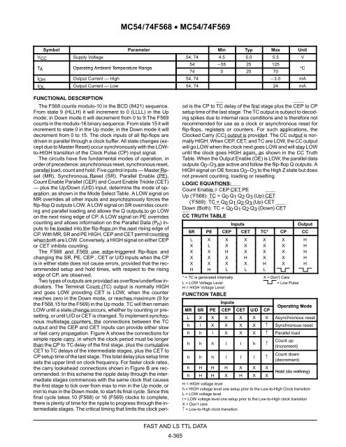
MC54/74F568 • MC54/74F569<br />
Symbol Parameter Min Typ Max Unit<br />
VCC Supply Voltage 54, 74 4.5 5.0 5.5 V<br />
TA<br />
Operating Ambient Temperature Range<br />
54 –55 25 125<br />
74 0 25 70<br />
°C<br />
IOH Output Current — High 54, 74 –3.0 mA<br />
IOL Output Current — Low 54, 74 24 mA<br />
FUNCTIONAL DESCRIPTION<br />
The F568 counts modulo-10 in the BCD (8421) sequence.<br />
From state 9 (HLLH) it will increment to 0 (LLLL) in the Up<br />
mode; in Down mode it will decrement from 0 to 9.The F569<br />
counts in the modulo-16 binary sequence. From state 15 it will<br />
increment to state 0 in the Up mode; in the Down mode it will<br />
decrement from 0 to 15. The clock inputs of all flip-flops are<br />
driven in parallel through a clock buffer. All state changes (except<br />
due to Master Reset) occur synchronously with the LOWto-HIGH<br />
transition of the Clock Pulse (CP) input signal.<br />
The circuits have five fundamental modes of operation, in<br />
order of precedence: asynchronous reset, synchronous reset,<br />
parallel load, count and hold. Five control inputs — Master Reset<br />
(MR), Synchronous Reset (SR), Parallel Enable (PE),<br />
Count Enable Parallel (CEP) and Count Enable Trickle (CET)<br />
— plus the Up/Down (U/D) input, determine the mode of operation,<br />
as shown in the Mode Select Table. A LOW signal on<br />
MR overrides all other inputs and asynchronously forces the<br />
flip-flop Q outputs LOW. A LOW signal on SR overrides counting<br />
and parallel loading and allows the Q outputs to go LOW<br />
on the next rising edge of CP. A LOW signal on PE overrides<br />
counting and allows information on the Parallel Data (Pn) inputs<br />
to be loaded into the flip-flops on the next rising edge of<br />
CP. With MR, SR and PE HIGH, CEP and CET permit counting<br />
when both are LOW. Conversely, a HIGH signal on either CEP<br />
or CET inhibits counting.<br />
The F568 and F569 use edge-triggered flip-flops and<br />
changing the SR, PE, CEP , CET or U/D inputs when the CP<br />
is in either state does not cause errors, provided that the recommended<br />
setup and hold times, with respect to the rising<br />
edge of CP, are observed.<br />
Two types of outputs are provided as overflow/underflow indicators.<br />
The Terminal Count (TC) output is normally HIGH<br />
and goes LOW providing CET is LOW, when the counter<br />
reaches zero in the Down mode, or reaches maximum (9 for<br />
the F568,15 for the F569) in the Up mode. TC will then remain<br />
LOW until a state change occurs, whether by counting or presetting,<br />
or until U/D or CET is changed. To implement synchronous<br />
multistage counters, the connections between the TC<br />
output and the CEP and CET inputs can provide either slow<br />
or fast carry propagation. Figure A shows the connections for<br />
simple ripple carry, in which the clock period must be longer<br />
than the CP to TC delay of the first stage, plus the cumulative<br />
CET to TC delays of the intermediate stages, plus the CET to<br />
CP setup time of the last stage. This total delay plus setup time<br />
sets the upper limit on clock frequency. For faster clock rates,<br />
the carry lookahead connections shown in Figure B are recommended.<br />
In this scheme the ripple delay through the intermediate<br />
stages commences with the same clock that causes<br />
the first stage to tick over from max to min in the Up mode, or<br />
min to max in the Down mode, to start its final cycle. Since this<br />
final cycle takes 10 (F568) or 16 (F569) clocks to complete,<br />
there is plenty of time for the ripple to progress through the intermediate<br />
stages. The critical timing that limits the clock period<br />
is the CP to TC delay of the first stage plus the CEP to CP<br />
setup time of the last stage. The TC output is subject to decoding<br />
spikes due to internal race conditions and is therefore not<br />
recommended for use as a clock or asynchronous reset for<br />
flip-flops, registers or counters. For such applications, the<br />
Clocked Carry (CC) output is provided. The CC output is normally<br />
HIGH. When CEP, CET, and TC are LOW, the CC output<br />
will go LOW when the clock next goes LOW and will stay LOW<br />
until the clock goes HIGH again, as shown in the CC Truth<br />
Table. When the Output Enable (OE) is LOW, the parallel data<br />
outputs O0–O3 are active and follow the flip-flop Q outputs. A<br />
HIGH signal on OE forces O0–O3 to the High Z state but does<br />
not prevent counting, loading or resetting.<br />
LOGIC EQUATIONS:<br />
Count Enable = CEP⋅CET⋅PE<br />
Up (’F568): TC = Q0⋅Q1⋅Q2⋅Q3⋅(Up)⋅CET<br />
(’F569): TC = Q0⋅Q1⋅Q2⋅Q3⋅(Up)⋅CET<br />
Down (Both): TC = Q0⋅Q1⋅Q2⋅Q3⋅(Down)⋅CET<br />
CC TRUTH TABLE<br />
Inputs<br />
Output<br />
SR PE CEP CET TC* CP CC<br />
L X X X X X H<br />
X L X X X X H<br />
X X H X X X H<br />
X X X H X X H<br />
X X X X H X H<br />
H H L L L<br />
* = TC is generated internally X = Don’t Care<br />
L = LOW Voltage Level<br />
= Low Pulse<br />
H = HIGH Voltage Level<br />
FUNCTION TABLE<br />
Inputs<br />
MR SR PE CEP CET U/D CP<br />
Operating Mode<br />
L X X X X X X Asynchronous reset<br />
h l X X X X ↑ Synchronous reset<br />
h h l X X X ↑ Parallel load<br />
h h h l l h ↑<br />
h h h l l l ↑<br />
h H H H X X X<br />
h H H X H X X<br />
Count up<br />
(increment)<br />
Count down<br />
(decrement)<br />
Hold (do nothing)<br />
H = HIGH voltage level<br />
h = HIGH voltage level one setup prior to the Low-to-High Clock transition<br />
L = LOW voltage level<br />
l = LOW voltage level one setup prior to the Low-to-High clock transition<br />
X = Don’t care<br />
↑ = Low-to-High clock transition<br />
FAST AND LS TTL DATA<br />
4-365