PMD-100
PMD-100
PMD-100

You also want an ePaper? Increase the reach of your titles
YUMPU automatically turns print PDFs into web optimized ePapers that Google loves.
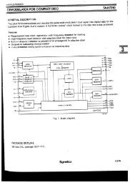
General Description<br />
®<br />
The <strong>PMD</strong>-<strong>100</strong> HDCD ® Process Decoder is a sophisticated<br />
0.6 micron CMOS Integrated Circuit that performs precise<br />
decoding of HDCD encoded recordings. The Decoder<br />
also functions as a state-of-the-art digital filter when fed<br />
data from non-HDCD recordings. It is designed to interface<br />
directly with popular data receivers and DAC’s, eliminates<br />
the need for conventional monolithic digital filters.<br />
The <strong>PMD</strong>-<strong>100</strong> has been carefully designed to maximize performance<br />
and ease of use in a wide variety of applications.<br />
HDCD Process Information<br />
Data encoded with HDCD process information carries precisely<br />
encrypted signals, hidden within the LSB of the 16-<br />
bit data word. Over time, only 1 to 5% of the LSB is used<br />
for this hidden code. The encoded information is inaudible<br />
and causes no perceptible loss of information. The<br />
<strong>PMD</strong>-<strong>100</strong> recognizes the encrypted signals as HDCD process<br />
information, and directs the decoding function to precisely<br />
reconstruct the high resolution signal in a form appropriate<br />
for output to the D-A converter being used.<br />
Note: To preserve HDCD process information, no alteration<br />
of the encoded data is allowed prior to processing by the <strong>PMD</strong>-<br />
<strong>100</strong>. Digital data processing including phase inversion prior to<br />
the <strong>PMD</strong>-<strong>100</strong> input will result in the loss of HDCD process<br />
information encoded in the data.<br />
SPECIAL FEATURES<br />
<strong>PMD</strong>-<strong>100</strong><br />
<strong>PMD</strong>-<strong>100</strong> Process Decoder<br />
Automatic HDCD Process Decoding<br />
When the <strong>PMD</strong>-<strong>100</strong> detects HDCD ® process information<br />
in the input data, it automatically switches to<br />
HDCD ® decode mode, and provides an output to drive<br />
an LED indicator. When non-HDCD ® process input<br />
data is received, the decoder automatically operates<br />
as a high performance digital filter.<br />
Excellent Filter Characteristics<br />
When operating as a digital filter, the <strong>PMD</strong>-<strong>100</strong> exhibits<br />
passband characteristics that have been carefully<br />
optimized to provide extremely accurate sound<br />
quality. Passband ripple from 0 to 20 kHz is within<br />
±.0001 dB and stopband attenuation is greater than<br />
120 dB.<br />
Two Operating Modes<br />
Stand-Alone<br />
In Stand-Alone Mode, the <strong>PMD</strong>-<strong>100</strong> requires no<br />
external controller, allowing for the most cost<br />
effective designs.<br />
Program<br />
In Program mode, an external processor controls<br />
the <strong>PMD</strong>-<strong>100</strong>’s many advanced operating modes<br />
and features.<br />
HDCD<br />
9300-0005<br />
Rev A1<br />
HDCD® and High Definition Compatible Digital®<br />
are registered trademarks of Pacific Microsonics, Inc<br />
Pacific Microsonics, Inc.<br />
32990 Alvarado Niles Road, Suite 910<br />
Union City, CA 94587<br />
Phone (510) 475-8000 Fax (510) 475-8005<br />
1
<strong>PMD</strong>-<strong>100</strong><br />
<strong>PMD</strong>-<strong>100</strong> Process Decoder<br />
®<br />
SPECIAL FEATURES (Cont.)<br />
DAC Optimize Operating Modes<br />
To achieve the best possible performance from a variety of<br />
different DAC types, adjustable parameters are provided including<br />
eight different levels of dither and Patented “Silent<br />
Conversion” variable clock timing.<br />
Constant Clock Output<br />
The <strong>PMD</strong>-<strong>100</strong> constantly provides output clocking to the DAC,<br />
even if input data and master clocks are lost. This feature eliminates<br />
the possiblility of spikes or DC offsets at the DAC’s output.<br />
Additional Features<br />
• 24 bit or greater accuracy provided for all operations.<br />
• Up to 24 bit input data passed without truncation.<br />
• 32 kHz to 55 kHz input data rates.<br />
• Output digital attenuation over a 96 dB range in<br />
0.188 dB steps.<br />
• Output soft mute and hard mute functions.<br />
• 16, 18, 20 or 24 bit output data.<br />
• 8 Fs, 4 Fs or 2 Fs output data rates. (Multiple<br />
output data rates are provided to allow flexible DAC<br />
operation and ease of use in designs that employ<br />
custom DSP based filters for non-HDCD ® process<br />
recordings.)<br />
• Digital domain deemphasis.<br />
• 256 Fs or 384 Fs system clock.<br />
Digital Characterisitcs<br />
V DD<br />
= 4.75V to 5.25V ,<br />
V SS<br />
= OV ,<br />
T A<br />
= 0°C to +70°C unless otherwise specified.<br />
2<br />
Pacific Microsonics, Inc.<br />
32990 Alvarado Niles Road, Suite 910<br />
Union City , CA 94587<br />
Phone (510) 475-8000 Fax (510) 475-8005
®<br />
<strong>PMD</strong>-<strong>100</strong><br />
<strong>PMD</strong>-<strong>100</strong> Process Decoder<br />
V DD<br />
= 4.75V to 5.25V ,<br />
V SS<br />
= OV ,<br />
T A<br />
= 0°C to +70°C unless otherwise specified.<br />
0<br />
Stopband Response<br />
Frequency kHz at 44.1 kHz sampling<br />
0.01<br />
Passband Response<br />
Frequency kHz at 44.1 kHz sampling<br />
Attenuation (dB)<br />
-20<br />
-40<br />
-60<br />
-80<br />
Amplitude (dB)<br />
0.005<br />
0<br />
-<strong>100</strong><br />
-0.005<br />
-120<br />
-140<br />
0 5 10 15 20 25 30 35 40<br />
-0.01<br />
0 5 10 15 20 25 30 35 40<br />
Pacific Microsonics, Inc.<br />
32990 Alvarado Niles Road, Suite 910<br />
Union City, CA 94587<br />
Phone (510) 475-8000 Fax (510) 475-8005<br />
3
<strong>PMD</strong>-<strong>100</strong><br />
<strong>PMD</strong>-<strong>100</strong> Process Decoder<br />
®<br />
Pin Description (Stand-Alone Mode) -<br />
Pin 9 Low<br />
( I = Input, O = Output. All input levels TTL compatible<br />
except XTI which must be CMOS level. No inputs have<br />
pull-ups. All outputs are full CMOS levels. )<br />
1: DIN (I) Serial data input.<br />
2: BCKI (I) Bit clock input.<br />
3: XTIM (I) Select system clock frequency.<br />
Low = 256 Fs, High = 384 Fs.<br />
4: DITH(I) Dither select.<br />
Low = dither disabled,<br />
High = dither added.<br />
5: GAIN (O) Analog output stage gain.<br />
Use only if Pin 19 is High (see page<br />
14).<br />
Low = low gain,<br />
High = high gain (+6 dB).<br />
(See pin 19 description).<br />
6: XTI (I) System clock input.<br />
7: VDD1 +5 volt power for filter.<br />
8: VSS1 Ground<br />
9: PROG(I) Select Program mode.<br />
Low = Stand-Alone,<br />
High = Program.<br />
Note: Pins 10 through 14 perform different functions<br />
depending on whether Stand-Alone or Program mode is<br />
selected.<br />
Stand-Alone Mode:<br />
10: OSIZ0 (I)<br />
11: OSIZ1 (I)<br />
These two pins determine the output word size, as well as<br />
the number of pulses on BCKO.<br />
12: COB (I) Output data format.<br />
Low = complementary offset binary,<br />
High = 2’s complement.<br />
13: JUST (I) Input data justification.<br />
Low = data assumed to be left justi<br />
fied up to 24 bits in length,<br />
High = data right justified 16 bits.<br />
14: BCPL (I) Input data latching.<br />
Low = input data latched on rising<br />
edge of BCKI. High = input data<br />
latched on falling edge of BCKI.<br />
15: SMUTE (I) Soft mute. Low = off, High = on.<br />
16: DEEMPH(I)De-emphasis filter.<br />
Low = off, High = on.<br />
17: HMUTE (I) Hard mute. Low = off, High = on.<br />
18: FSEL (I) De-emphasis filter Fs.<br />
Low = 44.1 kHz, High = 48 kHz.<br />
19: SCAL (I) Gain scaling.<br />
Low = 6dB gain scaling is performed<br />
internally in the digital domain,<br />
High = analog output gain stage is set<br />
by pin 5 GAIN. (See page 14.)<br />
20: DG (O) DAC sample and hold deglitch signal.<br />
21: VSS2 Ground. (Common with VSS1)<br />
22: VDD2 +5 volt power for output interface.<br />
23: DOR (O) Right channel serial data output.<br />
24: DOL (O) Left channel serial data output.<br />
25: WCKO(O) Word clock output.<br />
26: BCKO (O) Bit clock output.<br />
27: HDCD (O) HDCD encoding detect.<br />
Low = no encoding. High = HDCD<br />
encoded input data. (Output current<br />
rated at 12mA.)<br />
28: LRCI (I) Word clock input.<br />
4<br />
Pacific Microsonics, Inc.<br />
32990 Alvarado Niles Road, Suite 910<br />
Union City , CA 94587<br />
Phone (510) 475-8000 Fax (510) 475-8005
®<br />
<strong>PMD</strong>-<strong>100</strong><br />
<strong>PMD</strong>-<strong>100</strong> Process Decoder<br />
Pin Description (Program Mode) -<br />
Pin 9 High<br />
( I = Input, O = Output. All input levels TTL compatible<br />
except XTI which must be CMOS level. No inputs have<br />
pull-ups. All outputs are full CMOS levels. )<br />
1: DIN (I) Serial data input.<br />
2: BCKI (I) Bit clock input.<br />
3: XTIM (I) Select system clock frequency.<br />
Low = 256 Fs, High = 384 Fs.<br />
4: DITH(I) Dither select.<br />
Low = dither disabled,<br />
High = dither added.<br />
5: GAIN (O) Analog output stage gain.<br />
Use only if Pin 19 is High (see page<br />
14).<br />
Low = low gain,<br />
High = high gain (+6 dB).<br />
(See pin 19 description).<br />
6: XTI (I) System clock input.<br />
7: VDD1 +5 volt power for filter.<br />
8: VSS1 Ground<br />
9: PROG(I) Select Program mode.<br />
Low = Stand-Alone,<br />
High = Program.<br />
Note: Pins 10 through 14 perform different functions<br />
depending on whether Stand-Alone or Program mode is<br />
selected.<br />
Program Mode:<br />
10: MS1 (I) Mode set bit.<br />
11: MS2 (I) Mode set bit.<br />
12: MS3 (I) Mode set bit.<br />
13: MDT (I) Mode data.<br />
14: MEN (I) Mode enable.<br />
MS1, MS2 and MS3 form eight<br />
different three bit words which select<br />
the command mode. The next rising<br />
edge on MEN activates the selected<br />
mode. Data on MDT is entered us<br />
ing the SHIFT mode (See program<br />
mode description page 11.)<br />
15: SMUTE (I) Soft mute. Low = off, High = on.<br />
16: DEEMPH(I) De-emphasis filter.<br />
Low = off, High = on.<br />
17: HMUTE (I) Hard mute. Low = off, High = on.<br />
18: FSEL (I) De-emphasis filter Fs.<br />
Low = 44.1 kHz, High = 48 kHz.<br />
19: SCAL (I) Gain scaling.<br />
Low = 6dB gain scaling is performed<br />
internally in the digital domain,<br />
High = analog output gain stage is set<br />
by pin 5 GAIN. (See page 14).<br />
20: DG (O) DAC sample and hold deglitch sig<br />
nal.<br />
21: VSS2 Ground. (Common with VSS1)<br />
22: VDD2 +5 volt power for output interface.<br />
23: DOR (O) Right channel serial data output.<br />
24: DOL (O) Left channel serial data output.<br />
25: WCKO(O) Word clock output.<br />
26: BCKO(O) Bit clock output.<br />
27: HDCD (O) HDCD encoding detect.<br />
Low = no encoding. High = HDCD<br />
encoded input data. (Output current<br />
rated at 12mA.)<br />
28: LRCI (I) Word clock input.<br />
Pacific Microsonics, Inc.<br />
32990 Alvarado Niles Road, Suite 910<br />
Union City, CA 94587<br />
Phone (510) 475-8000 Fax (510) 475-8005<br />
5
<strong>PMD</strong>-<strong>100</strong><br />
<strong>PMD</strong>-<strong>100</strong> Process Decoder<br />
®<br />
Timing Characteristics<br />
The <strong>PMD</strong>-<strong>100</strong> is designed as a synchronous circuit, which means that it uses a master clock input XTI which is always<br />
synchronized with and typically derived from the input data stream. The master clock frequency can be either 256 or 384<br />
times the input sampling frequency (256 Fs or 384 Fs). If XTIM is low (XTI = 256 Fs), XTI must be between 8.192 and<br />
14.1312 MHz with a 33 to 67% duty cycle. If XTIM is high (XTI = 384 Fs), XTI must be between 12.288 and 18.432<br />
MHz with a 33 to 67% duty cycle, or between 18.432 and 21.1968 MHz with a 40 to 60% duty cycle. A selection of<br />
timing values are as follows:<br />
The <strong>PMD</strong>-<strong>100</strong> constantly provides WCKO and BCKO outputs even if input data (DIN) and/or master clock (XTI) is lost.<br />
This constant clock output eliminates the possiblility of spikes or DC offsets at the DAC’s output. It is recommended that<br />
if DIN or XTI are lost, hard mute (HMUTE) is enabled to prevent invalid data output. If the chip detects a synchronization<br />
error between the master clock (XTI) and the input word clock (LRCI) it automatically exerts a hard mute internally.<br />
Input Detailed Timing<br />
Stand-Alone or Programmed Mode<br />
T1 and T2 should be examined with a ‘scope to ascertain compliance. If necessary, an<br />
inverter stage should be added between the <strong>PMD</strong>-<strong>100</strong> XTI signal and the LRCI source<br />
to correct any observed error. (See Fig. 1.)<br />
Note: that the timing diagrams display the worst case scenario and actual performance should be better.<br />
6<br />
Pacific Microsonics, Inc.<br />
32990 Alvarado Niles Road, Suite 910<br />
Union City , CA 94587<br />
Phone (510) 475-8000 Fax (510) 475-8005
®<br />
<strong>PMD</strong>-<strong>100</strong><br />
<strong>PMD</strong>-<strong>100</strong> Process Decoder<br />
Data Input<br />
The input data word format is MSB first, 16 to 24-bit left justified or 16 bit right justified (selected by JUST).<br />
Left and right channel data words are input alternately, with the left channel first. Refer to the Input Timing diagram below.<br />
Each serial input data bit is shifted into the serial to parallel conversion register on the rising or falling edge (selected by<br />
BCPL) of the BCKI bit clock input. The parallel data output is alternatively latched into the left and right channel input<br />
registers respectively on the rising and falling edges of the LRCI clock. The number of BCKI active edges must be 16, 18,<br />
20, 24, or more while LRCI is low or LRCI is high. The polarity of the LRCI clock is selected by LRPL. In Stand-Alone<br />
Mode, LRPL default is low. If LRPL is low, the rising edge of LRCI indicates the start of the data input cycle. Left channel<br />
data is input while LRCI is high and latched on the falling edge. Right channel data is then input while LRCI is low, and<br />
latched on the rising edge. If LRPL is high, the clock polarity is reversed and the falling edge of LRCI indicates the start of<br />
the data input cycle.<br />
The group (data input-to-output) delay is 83 input samples. This is measured from the active edge of LRCI preceding the<br />
input data, to the active edge of LRCI preceding the same phase output data. The group delay is the same with 2 Fs, 4 Fs<br />
or 8 Fs operation.<br />
When the input data format is I 2 S, the word clock is received one bit clock too early. A simple method for delaying the word<br />
clock for proper timing is to use a logic device to delay the word clock until it is triggered by the rising edge of the bit clock.<br />
(See Application Notes pg.s 16-20).<br />
Input Timing<br />
Stand-Alone or Programmed Mode<br />
RIGHT<br />
RIGHT<br />
Pacific Microsonics, Inc.<br />
32990 Alvarado Niles Road, Suite 910<br />
Union City, CA 94587<br />
Phone (510) 475-8000 Fax (510) 475-8005<br />
7
<strong>PMD</strong>-<strong>100</strong><br />
<strong>PMD</strong>-<strong>100</strong> Process Decoder<br />
®<br />
Data Output<br />
The output data format is determined by the oversampling rate and the word length. The oversampling rate of 2 Fs, 4 Fs,<br />
or 8 Fs is selected by OVER1 and OVER0. The default in Stand-Alone Mode is 8Fs. The output word length of 16, 18, 20,<br />
or 24 bits is selected by OSIZ1 and OSIZ0. This selection also determines the number of pulses on the BCKO bit clock<br />
output. Note that if OVER0 and OVER1 are set to 2 Fs, then OSIZ0 and OSIZ1 must be set to 24 bits and DITH<br />
must be set low (dither disabled).<br />
Refer to the Output Timing diagrams below; DOL and DOR are the left and right channel data outputs. Output data is<br />
MSB first and is selectable by COB to be either 2’s complement or complementary offset binary. Data is clocked out on the<br />
falling edge and latched on the rising edge of the BCKO bit clock output. There are as many bit clock rising edges as there<br />
are output data bits. The data word start is marked by the rising or falling edge (selected by WCPL) of the word clock<br />
output WCKO. The default setting for WCKO is the falling edge. After the last bit of the data word is output, the BCKO<br />
signal is halted, and remains in this mode until WCKO changes state and the DAC initiates D/A conversion. This “Silent<br />
Conversion” minimizes conversion jitter and ground bounce by allowing time for the DAC substrate noise to settle out<br />
prior to conversion.<br />
There are 32 deglitch intervals dividing the output sampling period. In Stand Alone Mode DG goes low at the beginning<br />
of the 15th interval and high at the beginning of the 31st interval. In Program Mode variable deglitch timing is available.<br />
The falling and rising edges can be programmed to occur at any of the 32 deglitch intervals as defined by DGL4, DGL3,<br />
DGL2, DGL1, and DGL0 (falling edge) and by DGH4, DGH3, DGH2, DGH1, and DGH0 (rising edge). (See: Program<br />
Mode).<br />
8 Fs Output Timing<br />
Stand-Alone Mode (PROG Pin = 0)<br />
WCKO<br />
8<br />
Pacific Microsonics, Inc.<br />
32990 Alvarado Niles Road, Suite 910<br />
Union City , CA 94587<br />
Phone (510) 475-8000 Fax (510) 475-8005
®<br />
<strong>PMD</strong>-<strong>100</strong><br />
<strong>PMD</strong>-<strong>100</strong> Process Decoder<br />
Output Detailed Timing<br />
Stand-Alone or Programmed Mode<br />
8 Fs Output Timing<br />
Programmed Mode (PROG Pin = 1)<br />
50<br />
Pacific Microsonics, Inc.<br />
32990 Alvarado Niles Road, Suite 910<br />
Union City, CA 94587<br />
Phone (510) 475-8000 Fax (510) 475-8005<br />
9
<strong>PMD</strong>-<strong>100</strong><br />
<strong>PMD</strong>-<strong>100</strong> Process Decoder<br />
®<br />
4 Fs Output Timing<br />
Programmed Mode (PROG Pin = 1)<br />
2 Fs Output Timing<br />
Programmed Mode (PROG Pin = 1)<br />
10<br />
Pacific Microsonics, Inc.<br />
32990 Alvarado Niles Road, Suite 910<br />
Union City , CA 94587<br />
Phone (510) 475-8000 Fax (510) 475-8005
®<br />
<strong>PMD</strong>-<strong>100</strong><br />
<strong>PMD</strong>-<strong>100</strong> Process Decoder<br />
Program Mode<br />
Important: In Program mode (PROG pin 9 high) the mode enable input clock (MEN pin 14), which enters data and<br />
commands on its rising edge, must remain high after the last command is executed, as shown in the timing diagram.<br />
Bringing it low again can cause the equivalent of a soft mute, or other anomalies.<br />
The modes set by the three inputs MS3, MS2 and MS1 are described below: (High = 1, Low = 0).<br />
Pacific Microsonics, Inc.<br />
32990 Alvarado Niles Road, Suite 910<br />
Union City, CA 94587<br />
Phone (510) 475-8000 Fax (510) 475-8005<br />
11
<strong>PMD</strong>-<strong>100</strong><br />
<strong>PMD</strong>-<strong>100</strong> Process Decoder<br />
®<br />
Mode Control<br />
The 24-bit mode control flag entered on pin 13 MDT has<br />
the names and functions listed below: (Data is entered in<br />
the order listed. Multiple bit fields, such as OVER are entered<br />
LSB first (OVER0). Refer to the Mode Control Register<br />
diagram.<br />
OVER0, OVER1:<br />
00 (Not used)<br />
10 Output data oversampling rate is 2 Fs.<br />
01 Output data oversampling rate is 4 Fs.<br />
11 Output data oversampling rate is 8 Fs.*<br />
BCPL:<br />
0 Input data is latched on BCKI rising edge.<br />
1 Input data is latched on BCKI falling edge.<br />
JUST:<br />
0 Input data is left justified up to 24 bits.<br />
1 Input data is right justified, assumed to be<br />
16 bits.<br />
WCPL:<br />
0 Output word boundry is on WCKO falling edge.*<br />
1 Output word boundry is on WCKO rising edge.<br />
COB:<br />
0 2’s complement output data.<br />
1 Complementary offset binary output data.<br />
DGL0, DGL1, DGL2, DGL3, DGL4:<br />
The falling edge of DG can be programmed to occur<br />
at the beginning of any one of 32 deglitch intervals<br />
dividing the output sampling period. This five bit<br />
word selects the falling edge of the deglitch interval.<br />
(In Stand-Alone Mode, DG goes low at the beginning<br />
of the 15th interval).<br />
DGH0, DGH1, DGH2, DGH3, DGH4:<br />
The rising edge of DG can be programmed to occur<br />
at any one of 32 deglitch intervals dividing the<br />
output sampling period. This five bit word selects<br />
the rising edge of the deglitch interval. (In Stand-<br />
Alone Mode, DG goes high at the beginning of the<br />
31st interval).<br />
LRPL:<br />
0 LRCI rising edge is the start edge.*<br />
1 LRCI falling edge is the start edge.<br />
OSIZ0, OSIZ1:<br />
00 Output word length is 16 bits.<br />
10 Output word length is 18 bits.<br />
01 Output word length is 20 bits.<br />
11 Output word length is 24 bits.<br />
DITH0, DITH1, DITH2:<br />
000 Dither mode 0.<br />
Minimum high frequency weighted*<br />
<strong>100</strong> Dither mode 1.<br />
010 Dither mode 2.<br />
110 Dither mode 3.<br />
001 Dither mode 4.<br />
101 Dither mode 5.<br />
011 Dither mode 6.<br />
Maximum high frequency weighted.<br />
111 Dither mode 7.<br />
Minimum white triangular PDF dither.<br />
RESA:<br />
0 Reserved, must be set to 0.<br />
RESB:<br />
0 Reserved, must be set to 0.<br />
RESB is the last bit entered.<br />
*Denotes default value in Stand-Alone Mode.<br />
Mode Control Register<br />
12<br />
Pacific Microsonics, Inc.<br />
32990 Alvarado Niles Road, Suite 910<br />
Union City , CA 94587<br />
Phone (510) 475-8000 Fax (510) 475-8005
®<br />
<strong>PMD</strong>-<strong>100</strong><br />
<strong>PMD</strong>-<strong>100</strong> Process Decoder<br />
Attenuation Mode<br />
In Program mode, the <strong>PMD</strong>-<strong>100</strong> has a digital attenuator which can be set for each channel in increments of 0.188 dB<br />
between 0 and approximately 96 dB of attenuation. The attenuation value is entered MSB first as a 9 bit word on the<br />
MDT pin. The same value attenuation may be clocked to both left and right registers by the use of the attenuators mode<br />
controls (see timing diagram below). Changes in attenuation value are always carried out smoothly at a rate of one 0.188<br />
dB step every 16 input samples. The delay between an attenuation command and the first sample it affects can be<br />
between 84 and <strong>100</strong> input samples.<br />
Since the <strong>PMD</strong>-<strong>100</strong> has no reset pin, when it is powered up in Program mode, the attenuator registers will contain<br />
arbitrary values. As part of the initial programming, it is necessary to issue a ZERO attenuation command or set the<br />
attenuation to known value using the SET LEFT and SET RIGHT commands.<br />
Attenuation Data Byte Attenuation Attenuation Data Byte Attenuation<br />
0 0000 0000 0 dB 0 0010 0000 6.016 dB<br />
0 0000 0001 0.188 dB 0 0011 0101 9.964 dB<br />
0 0000 0110 1.128 dB 0 0<strong>100</strong> 0000 12.032 dB<br />
0 0000 1011 2.068 dB 0 <strong>100</strong>0 0000 24.064 dB<br />
0 0001 0000 3.008 dB 1 0000 0000 48.128 dB<br />
1 1111 1111 96.068dBs<br />
Attenuation Register<br />
Muting<br />
The chip has two muting functions, hard mute and soft mute, which are activated by raising the respective input pins<br />
HMUTE and SMUTE to logic high. The soft mute ramps the output signal down at the same rate as the digital<br />
attenuator (one step per 16 input samples). It is designed for voluntary muting, such as when changing input selection.<br />
The hard mute goes to full attenuation in approximately 1millisecond, which is less than the group delay through the<br />
filter, and is intended to be used for emergency situations such as loss of input signal. Both muting functions release<br />
softly, at the rate of the digital attenuator. When combined with the fact that the chip continues to supply clock signals<br />
to the DAC’s in the absence of input signals, the digital muting may eliminate the need for analog muting in many circuit<br />
designs. Note that during soft mute, the output dither remains on, while during hard mute, output dither is off.<br />
Pacific Microsonics, Inc.<br />
32990 Alvarado Niles Road, Suite 910<br />
Union City, CA 94587<br />
Phone (510) 475-8000 Fax (510) 475-8005<br />
13
<strong>PMD</strong>-<strong>100</strong><br />
<strong>PMD</strong>-<strong>100</strong> Process Decoder<br />
®<br />
Dither Modes<br />
The <strong>PMD</strong>-<strong>100</strong> provides 8 different output dithers in Program mode. All dither levels are available for output data<br />
widths from 16 to 24 bits at 8 Fs and 4 Fs oversampling rates only. Dither must be disabled if the 2 Fs oversampling rate<br />
is selected (as well as 24 bit mode must be selected when the 2 Fs oversampling rate is selected). There are seven levels<br />
of high-frequency weighted dither (modes 0-6) plus minimum amplitude white triangular PDF dither (mode 7). Modes<br />
0 and 7 are minimum amplitude dithers which correct quantizing errors only, whereas modes 1 through 6 are increasing<br />
levels of high-frequency weighted dither designed to smooth out non-linearity errors in multi-bit DAC’s (Modes 0 or 7<br />
are appropriate for single-bit DAC’s). The HF weighted dithers put the dither energy above the audio spectrum, where<br />
most of it is later filtered out by the analog low-pass filter following the DAC. In general, multi-bit DAC’s behave better<br />
with high levels of dither, but some analog circuits following the DAC may have problems with transient intermodulation<br />
distortion (TIM) when confronted with high levels of high frequency energy. The best dither level for a particular circuit<br />
implementation must be determined empirically.<br />
Dither Notes:<br />
1) Dither level 6 is the highest level of high-frequency weighted dither available with the <strong>PMD</strong>-<strong>100</strong>.<br />
2) In Stand-Alone Mode, dither mode 0 (minimum high frequency weighted) is available. Setting pin 4 DITH low<br />
will disable all dither including programmed dither and should be used only for test purposes.<br />
Gain and Scale<br />
The <strong>PMD</strong>-<strong>100</strong> has a design attenuation of 1 dB to allow for filter overshoot on transients.<br />
Most HDCD recordings are encoded using peak extension which gives them more “head room” than standard 16 bit<br />
recordings. In order to ensure that the average program output level of most HDCD recordings match that of standard<br />
recordings, it is necessary to increase the gain of the system 6 dB for those HDCD recordings, or, equivalently, reduce the<br />
gain of standard recordings 6 dB. This can be done either in the analog domain after the DAC’s, which allows the full range<br />
of the DAC’s to be used for both types of recordings, or in the digital domain within the <strong>PMD</strong>-<strong>100</strong>.<br />
Note that one or the other of these gain scaling options must be used.<br />
If the designer elects to use the analog approach, a 6 dB glitch-free gain change, controlled by the GAIN output of the chip,<br />
must be provided in the analog circuit. In this case, the SCAL pin is tied high. Since HDCD recordings can have peaks<br />
which are 6 dB higher than standard recordings with the same average levels, the analog circuits must provide enough head<br />
room for these higher levels. The gain change switching in the analog circuitry should occur within 50 msec of the GAIN<br />
output change to insure proper audio output levels.<br />
To elect the digital scaling option, the SCAL pin is tied low and the GAIN pin must be left open. In this case, standard 16<br />
bit recordings and those HDCD recordings encoded without peak extension are attenuated 6 dB inside the chip. The<br />
digital implementation has the advantage of simplicity and the lack of audible glitches, but does not use 1 bit of DAC<br />
resolution on non-HDCD recordings. If 20 bit DAC’s are used, especially in conjunction with the <strong>PMD</strong>-<strong>100</strong>’s output<br />
dither options, this does not represent much of a loss in practice since standard recordings only have 16 bit resolution.<br />
However, if 20 or 24-bit signal sources are expected, gain scaling is best accomplished in the analog domain.<br />
De-emphasis Filter<br />
The purpose of the digital de-emphasis filter is to reduce high-frequency quantization noise and to increase dynamic<br />
range with pre-emphasized non-HDCD encoded recordings. De-emphasis is turned ON by setting the DEEMPH<br />
input HIGH. The filter coefficients are selected for the input data sample frequency (44.1 or 48 kHz) by setting the<br />
FSEL mode control flag.<br />
14<br />
Pacific Microsonics, Inc.<br />
32990 Alvarado Niles Road, Suite 910<br />
Union City , CA 94587<br />
Phone (510) 475-8000 Fax (510) 475-8005
®<br />
<strong>PMD</strong>-<strong>100</strong><br />
<strong>PMD</strong>-<strong>100</strong> Process Decoder<br />
Additional <strong>PMD</strong>-<strong>100</strong> Considerations<br />
Power and Ground<br />
VDD1 (pin 7) powers the core. VDD2 (pin 22) powers the output pins. VDD1 may be connected to VDD2 externally.<br />
For lowest output clock jitter, it is recommended that VDD 2<br />
be powered from it’s own separately regulated power supply.<br />
VSS1 (pin 8) and VSS2 (pin 21) are internally connected and must be externally connected to the same ground source.<br />
Adding a 0.1uF capacitor on each VDD-VSS pair, as close to these pins as possible, is strongly recommended.<br />
Input Pins<br />
Some of the input pins, such as HMUTE (pin 17) can produce several 10’s of microamps of noise current when pulled low.<br />
Because these inputs have TTL compatible input thresholds, this current can produce false triggering of logic high unless<br />
the impedance to ground is less than <strong>100</strong>0 ohms. If these inputs are driven by logic or pulled low to ground with a switch,<br />
there is no problem.<br />
Serial Data Input<br />
Due to the high-speed characteristics of the <strong>PMD</strong>-<strong>100</strong>, care should be taken to minimize high-frequency noise on the serial<br />
data and clock inputs. The <strong>PMD</strong>-<strong>100</strong> operates at TTL level thresholds and even very narrow spikes over 0.5V may be<br />
interpreted as valid data. Input data to the <strong>PMD</strong>-<strong>100</strong> should be properly terminated, either by series termination at the<br />
source, or if necessary, AC termination at the <strong>PMD</strong>-<strong>100</strong> input. Series termination may be especially helpful for the master<br />
clock source, XTI. A <strong>100</strong> ohm resistor in series with the XTI signal, as close to the source as possible, will help to prevent<br />
undershoot and potential lock-up. Also, pay close attention to the timing relationship of XTI relative to LRCI.<br />
Output Clocking<br />
Although every effort has been made to keep the internally generated jitter low in the <strong>PMD</strong>-<strong>100</strong>, for the best sonic<br />
performance we recommend re-clocking the critical conversion clock(s) using external circuitry. Don’t forget to maintain<br />
the timing relationships of the word clock, bit clock, and the right and left data outputs. The simplest thing to do is to just<br />
re-clock all of these output signals. When used as a low jitter filter without external re-clocking, the <strong>PMD</strong>-<strong>100</strong> should<br />
have its own power regulator and a 10uf in parallel with a 0.1uf decoupling capacitor for each power pin. Although the<br />
<strong>PMD</strong>-<strong>100</strong> accepts either 256 or 384 Fs, it’s output timing is based upon a 256 Fs system clock with a changing duty cycle.<br />
The <strong>PMD</strong>-<strong>100</strong> incorporates the Patented “Silent Conversion” variable clock timing and was designed to output a very<br />
stable word clock. These features resulted in minimizing jitter induced sonic degradation. However, the <strong>PMD</strong>-<strong>100</strong> was<br />
designed prior to the introduction of bit clocked DACs. Therefore, additional care must be used when implementing the<br />
<strong>PMD</strong>-<strong>100</strong> and any bit clocked DAC. In general, the <strong>PMD</strong>-<strong>100</strong> exhibits more jitter on it’s bit clock output when<br />
compared to it’s word clock output.<br />
The <strong>PMD</strong>-<strong>100</strong>’s internally generated jitter on the bit clock output is lower when it is operated at 256 Fs when compared<br />
to 384 Fs (XTIM low versus high). When implementing the <strong>PMD</strong>-<strong>100</strong> into a 384 Fs and bit clocked DAC design, we<br />
strongly recommend using re-clocking circuitry in order to attain the best possible sonic perfomance. To assure jitter-free<br />
conversion, digital signals should be reclocked directly from an oscillator placed near the DAC(s). By selecting a 768 Fs<br />
system clock to synchronize the re-clocking circuitry, then divide the system clock by two (using a flip-flop) which yields<br />
the desired 384 Fs system clock to drive the rest of the circuitry. For additional details on this implementation of the<br />
<strong>PMD</strong>-<strong>100</strong>, please contact Pacific Microsonics.<br />
Pacific Microsonics, Inc.<br />
32990 Alvarado Niles Road, Suite 910<br />
Union City, CA 94587<br />
Phone (510) 475-8000 Fax (510) 475-8005<br />
15
<strong>PMD</strong>-<strong>100</strong><br />
<strong>PMD</strong>-<strong>100</strong> Process Decoder<br />
®<br />
Application Notes<br />
YM3623B<br />
+5<br />
<strong>PMD</strong>-<strong>100</strong><br />
L/R<br />
BCO<br />
DO<br />
/oA<br />
15<br />
12<br />
17<br />
8<br />
LRCI<br />
BCKI<br />
DIN<br />
XTI<br />
XTIM<br />
+5<br />
ERR<br />
21<br />
DEP<br />
16<br />
22<br />
SEL<br />
S2<br />
24<br />
PROG<br />
JUST<br />
BCPL<br />
SMUTE<br />
HMUTE<br />
DEEMPH<br />
FSEL<br />
FIG. 1 Connecting <strong>PMD</strong>-<strong>100</strong> to the Yamaha YM3623B Digital Receiver<br />
CS8412<br />
<strong>PMD</strong>-<strong>100</strong><br />
17<br />
M3<br />
FSYNC<br />
11<br />
LRCI<br />
18<br />
M2<br />
SCK<br />
12<br />
BCKI<br />
24<br />
M1<br />
SDATA<br />
26<br />
DIN<br />
23<br />
M0<br />
MCK<br />
19<br />
XTI<br />
+5<br />
+5<br />
XTIM<br />
PROG<br />
16<br />
SEL<br />
ERF<br />
25<br />
JUST<br />
C0<br />
6<br />
BCPL<br />
Cc/F0<br />
3<br />
SMUTE<br />
HMUTE<br />
DEEMPH<br />
FSEL<br />
FIG. 2 Connecting the <strong>PMD</strong>-<strong>100</strong> to the Crystal CS8412 Digital Receiver<br />
16<br />
Pacific Microsonics, Inc.<br />
32990 Alvarado Niles Road, Suite 910<br />
Union City , CA 94587<br />
Phone (510) 475-8000 Fax (510) 475-8005
®<br />
<strong>PMD</strong>-<strong>100</strong><br />
<strong>PMD</strong>-<strong>100</strong> Process Decoder<br />
SAA7345<br />
+5<br />
<strong>PMD</strong>-<strong>100</strong><br />
16.9344 MHZ<br />
From D-A Converter<br />
WCLK<br />
SCLK<br />
20<br />
21<br />
D<br />
SET<br />
Q<br />
XTI<br />
LRCI<br />
13<br />
CRIN<br />
CLR<br />
Q<br />
BCKI<br />
DIN<br />
DATA<br />
19<br />
XTIM<br />
PROG<br />
JUST<br />
BCPL<br />
V5<br />
24<br />
SMUTE<br />
HMUTE<br />
DEEMPH<br />
FSEL<br />
From Processor<br />
FIG. 3 Connecting the <strong>PMD</strong>-<strong>100</strong> to the Phillips SAA7345 Demodulator I 2 s Mode<br />
16.9344 MHZ<br />
CXD 2515Q<br />
+5<br />
<strong>PMD</strong>-<strong>100</strong><br />
From D-A Converter<br />
LRCK<br />
BCLK<br />
DATA<br />
45<br />
47<br />
46<br />
LRCI<br />
BCKI<br />
DIN<br />
62<br />
XTAI<br />
XTI<br />
XTIM<br />
PROG<br />
MUTE<br />
EMPH<br />
79<br />
72<br />
JUST<br />
BCPL<br />
SMUTE<br />
HMUTE<br />
DEEMPH<br />
FSEL<br />
FIG. 4 Connecting the <strong>PMD</strong>-<strong>100</strong> to the Sony CXD2515Q Decoder EIAJ Mode<br />
Pacific Microsonics, Inc.<br />
32990 Alvarado Niles Road, Suite 910<br />
Union City, CA 94587<br />
Phone (510) 475-8000 Fax (510) 475-8005<br />
17
<strong>PMD</strong>-<strong>100</strong><br />
<strong>PMD</strong>-<strong>100</strong> Process Decoder<br />
®<br />
16.9344 MHZ<br />
CXD2517Q<br />
+5<br />
<strong>PMD</strong>-<strong>100</strong><br />
From D-A Converter<br />
LRCK<br />
BCK<br />
PCMD<br />
20<br />
22<br />
21<br />
LRCI<br />
BCKI<br />
DIN<br />
34<br />
XTAI<br />
XTI<br />
XTIM<br />
PROG<br />
MUTE<br />
EMPH<br />
48<br />
40<br />
JUST<br />
BCPL<br />
SMUTE<br />
HMUTE<br />
DEEMPH<br />
FSEL<br />
FIG. 5 Connecting the <strong>PMD</strong>-<strong>100</strong> to the Sony CXD2517Q<br />
16.9344 MHZ<br />
From D-A Converter<br />
CXD2518Q<br />
+5<br />
<strong>PMD</strong>-<strong>100</strong><br />
LRCK<br />
BCK<br />
PCMD<br />
42<br />
46<br />
44<br />
LRCI<br />
BCKI<br />
DIN<br />
73<br />
XTAI<br />
XTI<br />
XTIM<br />
PROG<br />
MUTE<br />
EMPH<br />
6<br />
62<br />
JUST<br />
BCPL<br />
SMUTE<br />
HMUTE<br />
DEEMPH<br />
FSEL<br />
FIG. 6 Connecting the <strong>PMD</strong>-<strong>100</strong> to the Sony CXD2518Q<br />
18<br />
Pacific Microsonics, Inc.<br />
32990 Alvarado Niles Road, Suite 910<br />
Union City , CA 94587<br />
Phone (510) 475-8000 Fax (510) 475-8005
®<br />
<strong>PMD</strong>-<strong>100</strong><br />
<strong>PMD</strong>-<strong>100</strong> Process Decoder<br />
16.9344 mHz From D-A Converter<br />
SAA7370A<br />
<strong>PMD</strong>-<strong>100</strong><br />
WCLK<br />
46<br />
LRCI<br />
SCLK<br />
48<br />
BCKI<br />
21<br />
CRIN<br />
DIN<br />
DATA<br />
45<br />
+5<br />
XTI<br />
XTIM<br />
PROG<br />
JUST<br />
BCPL<br />
V5<br />
40<br />
SMUTE<br />
HMUTE<br />
DEEMPH<br />
FSEL<br />
From Processor<br />
FIG. 7 Connecting the <strong>PMD</strong>-<strong>100</strong> to the Phillips SAA7370A Demodulator in EIJA Mode<br />
Control Register 3 @ 0011 set to 0010<br />
Control Register D @ 1101 set to 01xx<br />
<strong>PMD</strong>-<strong>100</strong><br />
+5<br />
HDCD<br />
(To Light)<br />
GAIN<br />
BCKO<br />
WCKO<br />
DOL<br />
DOR<br />
2<br />
1<br />
6<br />
CLOCK<br />
LE<br />
DATA<br />
PCM1702<br />
Low-Pass Filter<br />
Left Output<br />
DG<br />
SCALE<br />
DITH<br />
COB<br />
+5<br />
2<br />
1<br />
6<br />
CLOCK<br />
LE<br />
DATA<br />
PCM1702<br />
Low-Pass Filter<br />
Right Output<br />
OSIZ0<br />
OSIZ1<br />
FIG. 8 20 Bit / 8x Oversampled Conversion using the Burr-Brown PCM1702 DAC<br />
Pacific Microsonics, Inc.<br />
32990 Alvarado Niles Road, Suite 910<br />
Union City, CA 94587<br />
Phone (510) 475-8000 Fax (510) 475-8005<br />
19
<strong>PMD</strong>-<strong>100</strong><br />
<strong>PMD</strong>-<strong>100</strong> Process Decoder<br />
®<br />
<strong>PMD</strong>-<strong>100</strong><br />
XTI<br />
HDCD<br />
GAIN<br />
BCKO<br />
WCKO<br />
DOL<br />
DOR<br />
DG<br />
SCALE<br />
DITH<br />
COB<br />
OSIZ0<br />
OSIZ1<br />
(To Light)<br />
(Not Used)<br />
+5<br />
Low Jitter<br />
Crystal Oscillator<br />
or PLL<br />
PCM67 or PCM69<br />
12<br />
SYSTEM CLOCK<br />
11<br />
BCK<br />
13<br />
WDCK<br />
14<br />
DATA-L<br />
10<br />
DATA-R<br />
FIG. 9 18 Bit / 8x Oversampled Conversion using the Burr-Brown PCM67 or 69 DAC<br />
SM5864AP<br />
<strong>PMD</strong>-<strong>100</strong><br />
16.9344mHz<br />
26<br />
24<br />
CKO<br />
XTO<br />
XTI<br />
HDCD<br />
To Light<br />
GAIN<br />
Not Used<br />
23<br />
XTI<br />
BCKO<br />
1<br />
BCKI<br />
WCKO<br />
2<br />
WCKI<br />
DOL<br />
27<br />
DINL<br />
DOR<br />
28<br />
DINR<br />
DG<br />
SCALE<br />
+5<br />
+5<br />
3<br />
COMPN<br />
DITH<br />
25<br />
XDIVN<br />
COB<br />
20<br />
X3SL<br />
OSIZ0<br />
OSIZ1<br />
FIG. 10 20 Bit / 8x Conversion using the NPC SM5864AP DAC<br />
20<br />
Pacific Microsonics, Inc.<br />
32990 Alvarado Niles Road, Suite 910<br />
Union City , CA 94587<br />
Phone (510) 475-8000 Fax (510) 475-8005
®<br />
<strong>PMD</strong>-<strong>100</strong><br />
<strong>PMD</strong>-<strong>100</strong> Process Decoder<br />
Digital Filter Compatibility & Comparison<br />
The <strong>PMD</strong>-<strong>100</strong> HDCD ® Process Decoder is pin compatible with existing Digital Oversampling Filters: the NPC SM5842,<br />
NPC SM5803, and BB DF1700. Pin for pin, the data and clock input and output lines are as follows:<br />
Pin Name Description<br />
1 DIN Serial Data Input<br />
2 BCKI Bit Clock Input<br />
6 XTI System Clock Input<br />
23 DOR Right Channel Serial Data Output<br />
24 DOL Left Channel Serial Data Output<br />
25 WCKO Word Clock Output<br />
26 BCKO Bit Clock Output<br />
28 LRCI Word Clock Input<br />
A general comparison of the different digital filter specifications are outlined in the following table:<br />
Features <strong>PMD</strong>-<strong>100</strong> NPC NPC BB DF1700<br />
SM5842<br />
SM5803<br />
HDCD Process Decoding Yes No No No<br />
Operating Modes Both Stand-Alone only Program only Stand-Alone only<br />
(Program/Stand-Alone)<br />
Digital Attenuation 0-96dB (.188 steps) No 0-96dB (.188 steps) No<br />
Stopband Attenuation >120 dB >117 dB >110 dB >110 dB<br />
Dither Modes Choice of 8 1 only “Noise Shaping” None<br />
Oversampling Rates 8X, 4X, 2X 8X 8X, 4X 8X<br />
Input Word Length (bits) 16, 18, 20, 29 16, 18, 20, 24 16, 18 16<br />
Output Word Length (bits) 16, 18, 20, 24 18, 20, 22, 24 16, 18, 20 16, 18, 20<br />
System Clock (Fs) 256, 384 256, 384 192, 256, 384, 512 192, 256, 384, 512<br />
Input Sample Rate (kHz) 32 - 55 32, 44.1, 48 32, 44.1, 48 32, 44.1, 48<br />
Muting Hard & Soft Soft, L & R Soft, L & R None<br />
Independent Independent<br />
Digital Deemphasis Yes Yes Yes No<br />
“Jitter Free” Clocking Yes Yes Yes No<br />
Pacific Microsonics, Inc.<br />
32990 Alvarado Niles Road, Suite 910<br />
Union City, CA 94587<br />
Phone (510) 475-8000 Fax (510) 475-8005<br />
21
<strong>PMD</strong>-<strong>100</strong><br />
<strong>PMD</strong>-<strong>100</strong> Process Decoder<br />
®<br />
ELECTROSTATIC<br />
DISCHARGE SENSITIVITY<br />
Electrostatic discharge can cause damage ranging from<br />
performance degradation to complete device failure.<br />
Pacific Microsonics, Inc. recommends that all integrated<br />
circuits be handled and stored using appropriate ESD<br />
protection methods.<br />
(1) Not JEDEC Standard<br />
NOTE: Leads in true position<br />
within 0.01” (0.25mm) R at<br />
MMC at seating plane. Pin<br />
numbers shown for reference<br />
only. Numbers may not be<br />
marked on package.<br />
Pin Out for <strong>PMD</strong>-<strong>100</strong>CQ Stand-<br />
Alone Mode (for descriptions refer<br />
to Page 4)<br />
Pin # Signal<br />
Pin # Signal<br />
Pin # Signal<br />
Pin # Signal<br />
1: GAIN 12: COB<br />
2: XTI 13: JUST<br />
3: N.C. 14: N.C<br />
4: VDD 1a 15: BCPL<br />
5: VDD 1b 16: N.C.<br />
6: N.C. 17: SMUTE<br />
7: VSS 1a 18: N.C.<br />
8: VSS 1b 19: DEEMPH<br />
9: PROG 20: N.C.<br />
10: OSIZ0 21: HMUTE<br />
11: OSIZ1 22: FSEL<br />
23: SCAL 34: BCKO<br />
24: DG 35: HDCD<br />
25: N.C. 36: N.C.<br />
26: VSS 2a 37: LRCI<br />
27: VSS 2b 38: N.C.<br />
28: N.C. 39: DIN<br />
29: VDD 2a 40: N.C.<br />
30: VDD 2b 41: BCKI<br />
31: DOR 42: N.C.<br />
32: DOL 43: XTIM<br />
33: WCKO 44: DITH<br />
22<br />
Pacific Microsonics, Inc.<br />
32990 Alvarado Niles Road, Suite 910<br />
Union City , CA 94587<br />
Phone (510) 475-8000 Fax (510) 475-8005
®<br />
<strong>PMD</strong>-<strong>100</strong><br />
<strong>PMD</strong>-<strong>100</strong> Process Decoder<br />
Pin Out for <strong>PMD</strong>-<strong>100</strong>CQ Program<br />
Mode (for descriptions refer to Page 5)<br />
Pin # Signal<br />
Pin # Signal<br />
Pin # Signal<br />
Pin # Signal<br />
1: GAIN 12: MS 3<br />
2: XTI 13: MDT<br />
3: N.C. 14: N.C<br />
4: VDD 1a 15: MEN<br />
5: VDD 1b 16: N.C.<br />
6: N.C. 17: SMUTE<br />
7: VSS 1a 18: N.C.<br />
8: VSS 1b 19: DEEMPH<br />
9: PROG 20: N.C.<br />
10: MS 1 21: HMUTE<br />
11: MS 2 22: FSEL<br />
NOTE: N.C. means there is no internal connection to this pin.<br />
MECHANICAL<br />
TQFP44 (Thin quad flat pack package, 44 leads).<br />
23: SCAL 34: BCKO<br />
24: DG 35: HDCD<br />
25: N.C. 36: N.C.<br />
26: VSS 2a 37: LRCI<br />
27: VSS 2b 38: N.C.<br />
28: N.C. 39: DIN<br />
29: VDD 2a 40: N.C.<br />
30: VDD 2b 41: BCKI<br />
31: DOR 42: N.C.<br />
32: DOL 43: XTIM<br />
33: WCKO 44: DITH<br />
1.20 MAX<br />
SEATING<br />
PLANE<br />
SECTION A-A<br />
0.80<br />
1.00 REF<br />
1.00 ±0.05<br />
0.14 ±0.04<br />
0.25<br />
A<br />
44<br />
A<br />
10.00 BSC<br />
12.00 BSC<br />
0.15 MAX<br />
0.37 +0.08/-0.07<br />
DETAIL X<br />
0-7˚<br />
0.80 ±0.15<br />
1<br />
10.00<br />
12.00 ±0.25<br />
NOTES:<br />
1. DIMENSIONS ARE IN MILLIMETERS.<br />
2. LEADFRAME MATERIAL: COPPER.<br />
3. TO BE MOLDED CAVITY UP<br />
(SEE SECTION A-A).<br />
Pacific Microsonics, Inc.<br />
32990 Alvarado Niles Road, Suite 910<br />
Union City, CA 94587<br />
Phone (510) 475-8000 Fax (510) 475-8005<br />
23
<strong>PMD</strong>-<strong>100</strong><br />
<strong>PMD</strong>-<strong>100</strong> Process Decoder<br />
®<br />
HDCD Decoder Distributors<br />
United States<br />
Pacific Microsonics Inc.<br />
32990 Alvarado Niles Road, Suite 910<br />
Union City, CA 94587<br />
tel: 510 475 8000<br />
fax: 510 475 8005<br />
email: comments@hdcd.com<br />
Germany<br />
Rein Components GmbH<br />
Mr. Theo Görtz<br />
tel: +49 2153 733 111<br />
fax: +49 2153 733 371<br />
email: tgoertz@rnc.memec.com<br />
Scandinavia<br />
Micronor A/S<br />
Mr. Mogens Poulsen<br />
tel: +45 8681 6522<br />
fax: +45 8681 2827<br />
email: mogens.poulsen@micronor.dk<br />
United Kingdom and France<br />
Insight Technology Ltd.<br />
Mr. Jon Pippard<br />
tel: +44 1844 261 686<br />
fax: +44 1844 261 601<br />
email: jpippard@itl.memec.com<br />
Japan<br />
Takachiho Koheki Co. Ltd.<br />
Mr. Masa-aki Kanamatsu<br />
2-8, 1-chome, Yotsuya<br />
Shinju-ku, Tokyo 160<br />
tel: 81 3 3355 6695<br />
fax: 81 3 3357 5071<br />
email: hnishino@takachiho-kk.co.jp<br />
Spain<br />
Newtek Espana<br />
Mr. Jesus Martin Valbuena<br />
tel: +34 1 307 6893<br />
fax: +34 1 372 9453<br />
Benelux<br />
Memec Benelux<br />
17 Thame Park Road<br />
Thame, Oxon, OX 10 OBE<br />
tel: 44 1844 261 919<br />
fax: 44 1844 261 683<br />
email: svernmeulen@meb.memec.com<br />
Hong Kong<br />
Jetronic Technology Ltd.<br />
Mr. Thomas Wong<br />
Unit J, 7/F, World Tech Center<br />
95 How Ming Street, Kwun Tong<br />
Kowloon, HONG KONG<br />
tel: 852 2763 6806<br />
fax: 852 2790 2038<br />
email: tomswong@hkstar.com<br />
24<br />
Pacific Microsonics, Inc.<br />
32990 Alvarado Niles Road, Suite 910<br />
Union City , CA 94587<br />
Phone (510) 475-8000 Fax (510) 475-8005