AD1868* Single Supply Dual 18-Bit Audio DAC - VasilTech Audio
AD1868* Single Supply Dual 18-Bit Audio DAC - VasilTech Audio
AD1868* Single Supply Dual 18-Bit Audio DAC - VasilTech Audio

You also want an ePaper? Increase the reach of your titles
YUMPU automatically turns print PDFs into web optimized ePapers that Google loves.
a<br />
FEATURES<br />
<strong>Dual</strong> Serial Input, Voltage Output <strong>DAC</strong>s<br />
<strong>Single</strong> +5 V <strong>Supply</strong><br />
0.004% THD+N (typ)<br />
Low Power: 50 mW (typ)<br />
108 dB Channel Separation (min)<br />
Operates at 8 Oversampling<br />
16-Pin Plastic DIP or SOIC Package<br />
APPLICATIONS<br />
Portable Compact Disc Players<br />
Portable DAT Players and Recorders<br />
Automotive Compact Disc Players<br />
Automotive DAT Players<br />
Multimedia Workstations<br />
PRODUCT DESCRIPTION<br />
The AD<strong>18</strong>68 is a complete dual <strong>18</strong>-bit <strong>DAC</strong> offering excellent<br />
performance while requiring a single +5 V power supply. It is<br />
fabricated on Analog Devices’ ABCMOS wafer fabrication process.<br />
The monolithic chip includes CMOS logic elements, bipolar<br />
and MOS linear elements, and laser-trimmed thin-film<br />
resistor elements. Careful design and layout techniques have resulted<br />
in low distortion, low noise, high channel separation, and<br />
low power dissipation.<br />
The <strong>DAC</strong>s on the AD<strong>18</strong>68 chip employ a partially segmented<br />
architecture. The first three MSBs of each <strong>DAC</strong> are segmented<br />
into seven elements. The 15 LSBs are produced using standard<br />
R-2R techniques. The segments and R-2R resistors are laser<br />
trimmed to provide extremely low total harmonic distortion.<br />
The AD<strong>18</strong>68 requires no deglitcher or trimming circuitry. Low<br />
noise is achieved through the use of two noise-reduction capacitors.<br />
Each <strong>DAC</strong> is equipped with a high performance output amplifier.<br />
These amplifiers achieve fast settling and high slew rate,<br />
producing ±1 V signals at load currents up to ±1 mA. The<br />
buffered output signal range is 1.5 V to 3.5 V. Reference voltages<br />
of 2.5 V are provided, eliminating the need for “False<br />
Ground” networks.<br />
A versatile digital interface allows the AD<strong>18</strong>68 to be directly<br />
connected to all digital filter chips. Fast CMOS logic elements<br />
allow for an input clock rate of up to 13.5 MHz. This allows for<br />
operation at 2×, 4×, 8×, or 16× the sampling frequency for each<br />
channel. The digital input pins of the AD<strong>18</strong>68 are TTL and<br />
+5 V CMOS compatible.<br />
*Protected by U.S. Patent Numbers: 3,961,326; 4,141,004; 4,349,811;<br />
4,857,862; and patents pending.<br />
V L<br />
LL<br />
DL<br />
CK<br />
DR<br />
LR<br />
DGND<br />
V B R<br />
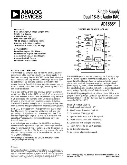
FUNCTIONAL BLOCK DIAGRAM<br />
1<br />
2<br />
3<br />
4<br />
5<br />
6<br />
7<br />
<strong>Single</strong> <strong>Supply</strong><br />
<strong>Dual</strong> <strong>18</strong>-<strong>Bit</strong> <strong>Audio</strong> <strong>DAC</strong><br />
<strong>AD<strong>18</strong>68*</strong><br />
<strong>18</strong>-BIT<br />
<strong>DAC</strong><br />
<strong>18</strong>-BIT<br />
SERIAL<br />
REGISTER<br />
<strong>18</strong>-BIT<br />
SERIAL<br />
REGISTER<br />
<strong>18</strong>-BIT<br />
<strong>DAC</strong><br />
AD<strong>18</strong>68<br />
–<br />
+<br />
V REF<br />
V REF<br />
+<br />
–<br />
8 9<br />
16<br />
15<br />
14<br />
13<br />
12<br />
11<br />
10<br />
V B L<br />
V S<br />
V O L<br />
NRL<br />
AGND<br />
The AD<strong>18</strong>68 operates on +5 V power supplies. The digital supply,<br />
V L , can be separated from the analog supply, V S , for reduced<br />
digital feedthrough. Separate analog and digital ground<br />
pins are also provided. In systems employing a single +5 volt<br />
power supply, V L and V S should be connected together. In battery<br />
operated systems, operation will continue even with reduced<br />
supply voltage. Typically, the AD<strong>18</strong>68 dissipates 50 mW.<br />
The AD<strong>18</strong>68 is packaged in either a 16-pin plastic DIP or a 16-<br />
pin plastic SOIC package. Operation is guaranteed over the temperature<br />
range of –35°C to +85°C and over the voltage supply<br />
range of 4.75 V to 5.25 V.<br />
PRODUCT HIGHLIGHTS<br />
1. <strong>Single</strong>-supply operation @ +5 V.<br />
2. 50 mW power dissipation (typical).<br />
3. THD+N is 0.004% (typical).<br />
4. Signal-to-Noise Ratio is 97.5 dB (typical).<br />
5. 108 dB channel separation (minimum).<br />
6. Compatible with all digital filter chips.<br />
7. 16-pin DIP and 16-pin SOIC packages.<br />
8. No deglitcher required.<br />
9. No external adjustments required.<br />
NRR<br />
V O R<br />
V S<br />
REV. A<br />
Information furnished by Analog Devices is believed to be accurate and<br />
reliable. However, no responsibility is assumed by Analog Devices for its<br />
use, nor for any infringements of patents or other rights of third parties<br />
which may result from its use. No license is granted by implication or<br />
otherwise under any patent or patent rights of Analog Devices.<br />
One Technology Way, P.O. Box 9106, Norwood, MA 02062-9106, U.S.A.<br />
Tel: 617/329-4700 Fax: 617/326-8703
AD<strong>18</strong>68–SPECIFICATIONS (typical at T A = +25C and +5 V supplies unless otherwise noted)<br />
Min Typ Max Units<br />
RESOLUTION <strong>18</strong> <strong>Bit</strong><br />
DIGITAL INPUTS V IH 2.4 V<br />
V IL 0.8 V<br />
I IH , V IH = V L 1.0 µA<br />
I IL , V IL = DGND 1.0 µA<br />
Maximum Clock Input Frequency 13.5 MHz<br />
ACCURACY<br />
Gain Error ±1 % of FSR<br />
Gain Matching ±1 % of FSR<br />
Midscale Error ±15 mV<br />
Midscale Error Matching ±10 mV<br />
Gain Linearity Error ±3 dB<br />
DRIFT (0°C to +70°C)<br />
Gain Drift ±100 ppm/°C<br />
Midscale Drift ±100 µV/°C<br />
TOTAL HARMONIC DISTORTION + NOISE<br />
0 dB, 990.5 Hz AD<strong>18</strong>68N 0.004 0.008 %<br />
AD<strong>18</strong>68N-J 0.004 0.006 %<br />
–20 dB, 990.5 Hz AD<strong>18</strong>68N 0.020 0.08 %<br />
AD<strong>18</strong>68N-J 0.020 0.08 %<br />
–60 dB, 990.5 Hz AD<strong>18</strong>68N 2.0 5.0 %<br />
AD<strong>18</strong>68N-J 2.0 5.0 %<br />
CHANNEL SEPARATION 1 kHz, 0 dB 108 NIL* dB<br />
SIGNAL-TO-NOISE RATIO (with A-Weight Filter) 95 97.5 dB<br />
D-RANGE (with A-Weight Filter) 86 92 dB<br />
OUTPUT<br />
Voltage Output Pins (V O L, V O R)<br />
Output Range (±3%) ±1 V<br />
Output Impedance 0.1 Ω<br />
Load Current ±1 mA<br />
Bias Voltage Pins (V B L, V B R)<br />
Output Voltage +2.5 V<br />
Output Impedance 350 Ω<br />
POWER SUPPLY<br />
Specification, V L and V S 4.75 5 5.25 V<br />
Operation, V L and V S 3.5 5.25 V<br />
+I, V L and V S = 5 V 10 14 mA<br />
POWER DISSIPATION 50 70 mW<br />
TEMPERATURE RANGE<br />
Specification 0 25 70 °C<br />
Operation –35 85 °C<br />
Storage –60 100 °C<br />
*Above 115 dB.<br />
Specifications subject to change without notice.<br />
ABSOLUTE MAXIMUM RATINGS*<br />
V L to DGND . . . . . . . . . . . . . . . . . . . . . . . . . . . . . . 0 V to 6 V<br />
V S to AGND . . . . . . . . . . . . . . . . . . . . . . . . . . . . . . 0 V to 6 V<br />
AGND to DGND . . . . . . . . . . . . . . . . . . . . . . . . . . . . ±0.3 V<br />
Digital Inputs to DGND . . . . . . . . . . . . . . . . . . . . . –0.3 to V L<br />
Soldering . . . . . . . . . . . . . . . . . . . . . . . . . . . . . +300°C, 10 sec<br />
*Stresses greater than those listed under “Absolute Maximum Ratings” may cause<br />
permanent damage to the device. This is a stress rating only and functional<br />
operation of the device at these or any other conditions above those indicated in the<br />
operational section of this specification is not implied. Exposure to absolute<br />
maximum rating conditions for extended periods may affect device reliability.<br />
CAUTION<br />
ESD (electrostatic discharge) sensitive device. Electrostatic charges as high as 4000 V readily<br />
accumulate on the human body and test equipment and can discharge without detection.<br />
Although the AD<strong>18</strong>68 features proprietary ESD protection circuitry, permanent damage may<br />
occur on devices subjected to high energy electrostatic discharges. Therefore, proper ESD<br />
precautions are recommended to avoid performance degradation or loss of functionality.<br />
–2–<br />
WARNING!<br />
ESD SENSITIVE DEVICE<br />
REV. A
THD +N – dB<br />
PSRR – dB<br />
THD +N – dB<br />
GAIN LINEARITY ERROR – dB<br />
THD +N – dB<br />
CHANNEL SEPARATION – dB<br />
AD<strong>18</strong>68<br />
Typical Performance of the AD<strong>18</strong>68<br />
–30<br />
150<br />
–40<br />
–60dB<br />
140<br />
–50<br />
–60<br />
130<br />
–70<br />
–20dB<br />
120<br />
–80<br />
–90<br />
0dB<br />
110<br />
–100<br />
0.5 2.5 4.5 6.5 8.5 10.5 12.5 14.5<br />
FREQUENCY – kHz<br />
16.5 <strong>18</strong>.5 20.5<br />
100<br />
10 3 10 4<br />
FREQUENCY – Hz<br />
Figure 1. THD+N vs. Frequency<br />
Figure 2. Channel Separation vs. Frequency<br />
–20<br />
8<br />
–30<br />
–60dB<br />
6<br />
0°C<br />
–40<br />
4<br />
–50<br />
–60<br />
2<br />
0<br />
25°C<br />
–70<br />
–80<br />
–20dB<br />
0dB<br />
–90<br />
4.4 4.6 4.8 5.0 5.2 5.4<br />
VOLTAGE SUPPLY<br />
–2<br />
70°C<br />
–4<br />
–6<br />
–100 –80 –60 –40 –20 –10<br />
INPUT AMPLITUDE – dB<br />
0<br />
Figure 3. THD+N vs. <strong>Supply</strong> Voltage<br />
Figure 4. Gain Linearity Error vs. Input Amplitude<br />
–20<br />
90<br />
–40<br />
– 60dB<br />
80<br />
70<br />
–60<br />
–80<br />
– 20dB<br />
0dB<br />
60<br />
50<br />
–100<br />
–50 –30 –10 10 30 50 70 90 110 130<br />
TEMPERATURE – °C<br />
Figure 5. THD+N vs. Temperature<br />
140<br />
40<br />
10 2 10 3 10 4 10 5<br />
SUPPLY MODULATION FREQUENCY – Hz<br />
Figure 6. Power <strong>Supply</strong> Rejection Ratio vs. Frequency<br />
REV. A –3–
AD<strong>18</strong>68<br />
V L<br />
LL<br />
DL<br />
CK<br />
DR<br />
LR<br />
DGND<br />
V B R<br />
PIN CONFIGURATION<br />
1<br />
2<br />
3<br />
4<br />
5<br />
6<br />
7<br />
AD<strong>18</strong>68<br />
TOP VIEW<br />
(Not To Scale)<br />
8 9<br />
16<br />
15<br />
14<br />
13<br />
12<br />
11<br />
10<br />
V B L<br />
V S<br />
V O L<br />
NRL<br />
AGND<br />
DEFINITION OF SPECIFICATIONS<br />
Total Harmonic Distortion + Noise<br />
Total harmonic distortion plus noise (THD+N) is defined as<br />
the ratio of the square root of the sum of the squares of the amplitudes<br />
of the harmonics and noise to the amplitude of the fundamental<br />
input frequency. It is usually expressed in percent (%)<br />
or decibels (dB).<br />
D-Range Distortion<br />
D-range distortion is the ratio of the amplitude of the signal at<br />
an amplitude of –60 dB to the amplitude of the distortion plus<br />
noise. In this case, an A-weight filter is used. The value specified<br />
for D-range performance is the ratio measured plus 60 dB.<br />
Signal-to-Noise Ratio<br />
The signal-to-noise ratio is defined as the ratio of the amplitude<br />
of the output when a full-scale output is present to the amplitude<br />
of the output with no signal present. It is expressed in<br />
decibels (dB) and measured using an A-weight filter.<br />
Gain Linearity<br />
Gain linearity is a measure of the deviation of the actual output<br />
amplitude from the ideal output amplitude. It is determined by<br />
measuring the amplitude of the output signal as the amplitude<br />
of that output signal is digitally reduced to a lower level. A perfect<br />
D/A converter exhibits no difference between the ideal and<br />
actual amplitudes. Gain linearity is expressed in decibels (dB).<br />
Midscale Error<br />
Midscale error is the difference between the analog output and<br />
the bias when the twos complement input code representing<br />
midscale is loaded in the input register. Midscale error is expressed<br />
in mV.<br />
NRR<br />
V O R<br />
V S<br />
PIN DESIGNATIONS<br />
11 V L Digital <strong>Supply</strong> (+5 Volts)<br />
12 LL Left Channel Latch Enable<br />
13 DL Left Channel Data Input<br />
14 CK Clock Input<br />
15 DR Right Channel Data Input<br />
16 LR Right Channel Latch Enable<br />
17 DGND Digital Common<br />
<strong>18</strong> V B R Right Channel Bias<br />
19 V S Analog <strong>Supply</strong> (+5 Volts)<br />
10 V O R Right Channel Output<br />
11 NRR Right Channel Noise Reduction<br />
12 AGND Analog Common<br />
13 NRL Left Channel Noise Reduction<br />
14 V O L Left Channel Output<br />
15 V S Analog <strong>Supply</strong> (+5 Volts)<br />
16 V B L Left Channel Bias<br />
FUNCTIONAL DESCRIPTION<br />
The AD<strong>18</strong>68 is a complete, voltage output dual <strong>18</strong>-bit digital<br />
audio <strong>DAC</strong> which operates with a single +5 volt supply. As<br />
shown in the block diagram, each channel contains a voltage<br />
reference, an <strong>18</strong>-bit <strong>DAC</strong>, an output amplifier, an <strong>18</strong>-bit input<br />
latch, and an <strong>18</strong>-bit serial-to-parallel input register.<br />
The voltage reference section provides a reference voltage and a<br />
false ground voltage for each channel. The low noise bandgap<br />
circuits produce reference voltages that are unaffected by<br />
changes in temperature, time, and power supply.<br />
The output amplifier uses both MOS and bipolar devices and<br />
incorporates an NPN class-A output stage. It is designed to produce<br />
high slew rate, low noise, low distortion, and optimal frequency<br />
response.<br />
Each <strong>18</strong>-bit <strong>DAC</strong> uses a combination of segmented decoder<br />
and R-2R architecture to achieve good integral and differential<br />
linearity. The resistors which form the ladder structure are fabricated<br />
with silicon-chromium thin film. Laser trimming of<br />
these resistors further reduces linearity error, resulting in low<br />
output distortion.<br />
The input registers are fabricated with CMOS logic gates.<br />
These gates allow fast switching speeds and low power consumption,<br />
contributing to the fast digital timing, low glitch, and<br />
low power dissipation of the AD<strong>18</strong>68.<br />
ORDERING GUIDE<br />
THD + N<br />
Package<br />
Model @ F S SNR Option*<br />
AD<strong>18</strong>68N 0.008% 95 dB N-16<br />
AD<strong>18</strong>68R 0.008% 95 dB R-16<br />
AD<strong>18</strong>68N-J 0.006% 95 dB N-16<br />
AD<strong>18</strong>68R-J 0.006% 95 dB R-16<br />
*N = Plastic DIP; R = SOIC.<br />
–4–<br />
REV. A
AD<strong>18</strong>68<br />
V L<br />
LL<br />
DL<br />
1<br />
2<br />
3<br />
<strong>18</strong>-BIT<br />
<strong>DAC</strong><br />
<strong>18</strong>-BIT<br />
SERIAL<br />
REGISTER<br />
AD<strong>18</strong>68<br />
–<br />
+<br />
16<br />
15<br />
14<br />
V B L<br />
V S<br />
V O L<br />
<strong>DAC</strong>, the AD<strong>18</strong>68 can continue to function at supply voltages<br />
as low as 3.5 V. Because of its unique design, the power requirements<br />
of the AD<strong>18</strong>68 diminish as the battery voltage drops, further<br />
extending the operating time of the system.<br />
POWER<br />
SUPPLY<br />
CK<br />
4<br />
V REF<br />
13<br />
NRL<br />
1<br />
AD<strong>18</strong>68<br />
V L<br />
V B L<br />
16<br />
DR<br />
LR<br />
5<br />
6<br />
<strong>18</strong>-BIT<br />
SERIAL<br />
REGISTER<br />
V REF<br />
12<br />
11<br />
AGND<br />
NRR<br />
0.1µF<br />
2<br />
3<br />
4<br />
LL<br />
DL<br />
CK<br />
V S<br />
V O L<br />
NRL<br />
15<br />
14<br />
13<br />
4.7µF<br />
0.1µF<br />
DGND<br />
V B R<br />
7<br />
<strong>18</strong>-BIT<br />
<strong>DAC</strong><br />
+<br />
–<br />
8 9<br />
10<br />
V O R<br />
V S<br />
5 DR AGND 12<br />
6<br />
7<br />
LR<br />
DGND<br />
NRR 11<br />
V O R 10<br />
8 V B R<br />
V S 9<br />
4.7µF<br />
Functional Block Diagram<br />
ANALOG CIRCUIT CONSIDERATIONS<br />
GROUNDING RECOMMENDATIONS<br />
The AD<strong>18</strong>68 has two ground pins, designated as AGND (Pin<br />
12) and DGND (Pin 7). The analog ground, AGND, serves as<br />
the “high quality” reference ground for analog signals and as a<br />
return path for the supply current from the analog portion of the<br />
device. The system analog common should be located as close<br />
as possible to Pin 12 to minimize any voltage drop which may<br />
develop between these two points, although the internal circuit<br />
is designed to minimize signal dependence of the analog return<br />
current.<br />
The digital ground, DGND, returns ground current from the<br />
digital logic portion of the device. This pin should be connected<br />
to the digital common node in the system. As shown in Figure<br />
7, the analog and digital grounds should be joined at one point<br />
in the system. When these two grounds are remotely connected<br />
such as at the power supply ground, care should be taken to<br />
minimize the voltage difference between the DGND and AGND<br />
pins in order to ensure the specified performance.<br />
POWER SUPPLIES AND DECOUPLING<br />
The AD<strong>18</strong>68 has three power supply input pins. V S (Pins 9 and<br />
15) provides the supply voltages which operate the analog portion<br />
of the device including the <strong>18</strong>-bit <strong>DAC</strong>s, the voltage references,<br />
and the output amplifiers. The V S supplies are designed<br />
to operate with a +5 V supply. These pins should be decoupled<br />
to analog common using a 0.1 µF capacitor. Good engineering<br />
practice suggests that the bypass capacitors be placed as close as<br />
possible to the package pins. This minimizes the inherent inductive<br />
effects of printed circuit board traces.<br />
V L (Pin 1) operates the digital portions of the chip including the<br />
input shift registers and the input latching circuitry. V L is also<br />
designed to operate with a +5 V supply. This pin should be bypassed<br />
to digital common using a 0.1 µF capacitor, again placed<br />
as close as possible to the package pin. Figure 7 illustrates the correct<br />
connection of the digital and analog supply bypass capacitors.<br />
An important feature of the AD<strong>18</strong>68 audio <strong>DAC</strong> is its ability to<br />
operate at reduced power supply voltages. This feature is very<br />
important in portable battery operated systems. As the batteries<br />
discharge, the supply voltage drops. Unlike any other audio<br />
Figure 7. Recommended Circuit Schematic<br />
NOISE REDUCTION CAPACITORS<br />
The AD<strong>18</strong>68 has two noise reduction pins designated as NRL<br />
(Pin 13) and NRR (Pin 11). It is recommended that external<br />
noise reduction capacitors be connected from these pins to<br />
AGND to reduce the output noise contributed by the voltage<br />
reference circuitry. As shown in Figure 7, each of these pins<br />
should be bypassed to AGND with a 4.7 µF or larger capacitor.<br />
The connections between the capacitors, package pins and<br />
AGND should be as short as possible to achieve the lowest<br />
noise.<br />
USING V B L AND V B R<br />
The AD<strong>18</strong>68 has two bias voltage reference pins, designated as<br />
V B R (Pin 8) and V B L (Pin 16). These pins supply a dc reference<br />
voltage equal to the center of the output voltage swing. These<br />
bias voltages replace “False Ground” networks previously required<br />
in single-supply audio systems. At the same time, they allow dccoupled<br />
systems, improving audio performance.<br />
Figure 8a illustrates the traditional approach used to generate<br />
False Ground voltages in single-supply audio systems. This circuit<br />
requires additional power and circuit board space.<br />
–V S<br />
DGND<br />
1<br />
2<br />
16-BIT<br />
LATCH<br />
16-BIT<br />
<strong>DAC</strong><br />
16<br />
15<br />
+V S<br />
TRIM<br />
+V L 3<br />
MSB<br />
SERIAL<br />
14<br />
ADJ<br />
INPUT<br />
REGISTER<br />
NC<br />
CLK<br />
4<br />
5<br />
I OUT 13<br />
12<br />
I OUT<br />
AGND<br />
CONTROL<br />
LOGIC<br />
LE<br />
DATA<br />
NC<br />
6<br />
7<br />
8<br />
11<br />
10<br />
9<br />
SJ<br />
R F<br />
V OUT<br />
AD<strong>18</strong>51<br />
NC = NO CONNECT<br />
Figure 8a. Schematic Using False Ground<br />
REV. A –5–
AD<strong>18</strong>68<br />
AD<strong>18</strong>68<br />
1<br />
2<br />
V L<br />
LL<br />
V B L 16<br />
V S<br />
15<br />
3<br />
4<br />
5<br />
6<br />
7<br />
DL<br />
CK<br />
DR<br />
LR<br />
DGND<br />
V O L 14<br />
NRL 13<br />
AGND 12<br />
NRR 11<br />
V O R 10<br />
8 VB R<br />
V S 9<br />
+ 5V<br />
+ 5V<br />
V O L<br />
V O R<br />
Figure 1 illustrates the typical THD+N versus frequency performance<br />
of the AD<strong>18</strong>68. It is evident that the THD+N performance<br />
of the AD<strong>18</strong>68 remains stable at all three levels through<br />
a wide range of frequencies. A load impedance of at least 2 kΩ is<br />
recommended for best THD+N performance.<br />
Analog Devices tests and grades all AD<strong>18</strong>68s on the basis of<br />
THD+N performance. During the distortion test, a high speed<br />
digital pattern generator transmits digital data to each channel<br />
of the device under test. Eighteen-bit data is latched into the<br />
<strong>DAC</strong> at 352.8 kHz (8× F S ). The test waveform is a 990.5 Hz<br />
sine wave with 0 dB, –20 dB, and –60 dB amplitudes. A 4096-<br />
point FFT calculates total harmonic distortion + noise,<br />
signal-to-noise ratio, and D-range. No deglitchers or external<br />
adjustments are used.<br />
Figure 8b. Circuitry Using Voltage Biases<br />
The AD<strong>18</strong>68 eliminates the need for “False Ground” circuitry.<br />
V B R and V B L generate the required bias voltages previously<br />
generated by the “False Ground.” As shown in Figure 8b, V B R<br />
and V B L may be used as the reference point in each output<br />
channel. This permits a dc-coupled output signal path. This<br />
eliminates ac-coupling capacitors and improves low frequency<br />
performance. It should be noted that these bias outputs have<br />
relatively high output impedance and will not drive output<br />
currents larger than 100 µA without degrading the specified<br />
performance.<br />
DISTORTION PERFORMANCE AND TESTING<br />
The THD+N figure of an audio <strong>DAC</strong> represents the amount of<br />
undesirable signal produced during reconstruction and playback<br />
of an audio waveform. Therefore, the THD+N specification<br />
provides a direct method to classify and choose an audio <strong>DAC</strong><br />
for a desired level of performance.<br />
DIGITAL CIRCUIT CONSIDERATIONS<br />
INPUT DATA<br />
The AD<strong>18</strong>68 digital input port employs five signals: Data Left<br />
(DL), Data Right (DR), Latch Left (LL), Latch Right (LR) and<br />
Clock (CLK). DL and DR are the serial inputs for the left and<br />
right <strong>DAC</strong>s, respectively. Input data bits are clocked into the input<br />
register on the rising edge of CLK. The falling edges of LL<br />
and LR cause the last <strong>18</strong> bits which were clocked into the serial<br />
registers to be shifted into the <strong>DAC</strong>s, thereby updating the respective<br />
<strong>DAC</strong> outputs. For systems using only a single latch signal,<br />
LL and LR may be connected together. For systems using<br />
only one DATA signal, DR and DL may be connected together.<br />
Data is transmitted to the AD<strong>18</strong>68 in a bit stream composed of<br />
<strong>18</strong>-bit words with a serial, twos complement, MSB first format.<br />
Left and right channels share the Clock (CLK) signal.<br />
Figure 9 illustrates the general signal requirements for data<br />
transfer for the AD<strong>18</strong>68.<br />
CLK<br />
DL<br />
MSB<br />
LSB<br />
DR<br />
MSB<br />
LSB<br />
LL<br />
LR<br />
Figure 9. Control Signals<br />
–6–<br />
REV. A
AD<strong>18</strong>68<br />
TIMING<br />
Figure 10 illustrates the specific timing requirements that must<br />
be met in order for the data transfer to be accomplished properly.<br />
The input pins of the AD<strong>18</strong>68 are TTL and 5 V CMOS<br />
compatible.<br />
The maximum clock rate of the AD<strong>18</strong>68 is specified to be at<br />
least 13.5 MHz. This clock rate allows data transfer rates of 2×,<br />
4×, 8×, and 16× F S (where F S equals 44.1 kHz). The applications<br />
section of this data sheet contains additional guidelines for<br />
using the AD<strong>18</strong>68.<br />
CLK<br />
DATA<br />
>30ns<br />
LATCH<br />
ENABLE (LE)<br />
> 74./ ns<br />
>30ns<br />
>30ns<br />
>10ns >10ns<br />
MSB<br />
1st BIT<br />
>60ns<br />
>40ns<br />
INTERNAL <strong>DAC</strong> INPUT REGISTER<br />
UPDATED WITH <strong>18</strong> MOST RECENT BITS<br />
2nd BIT<br />
LSB<br />
(<strong>18</strong>th BIT)<br />
Figure 10. Input Signal Timing<br />
>15ns<br />
>40ns<br />
NEXT<br />
WORD<br />
BITS CLOCKED<br />
TO SHIFT REGISTER<br />
APPLICATIONS OF THE AD<strong>18</strong>68<br />
The AD<strong>18</strong>68 is a high performance audio <strong>DAC</strong> specifically designed<br />
for portable and automotive digital audio applications.<br />
These market segments have technical requirements fundamentally<br />
different than those found in the high-end or home-use<br />
market segments. Portable equipment must rely on components<br />
which require low amounts of power to offer reasonable playing<br />
times. Also, battery voltages drop as the end of the discharge<br />
cycle is approached. The AD<strong>18</strong>68’s ability to operate from a<br />
single +5 V supply makes it a good choice for battery-operated<br />
gear. As the battery voltage drops, the power dissipation of the<br />
+5V POWER<br />
SUPPLY<br />
AD<strong>18</strong>68 drops. This extends the usable battery life. Finally, as<br />
the battery supply voltage drops, the bias voltages and signal<br />
swings also drop, preventing signal clipping and abrupt degradation<br />
of distortion. Figure 3 illustrates that THD+N performance<br />
of the AD<strong>18</strong>68 remains constant through a wide range<br />
of supply voltages.<br />
Automotive equipment rely on components which are able to<br />
consistently perform in a wide range of temperatures. In addition,<br />
due to the limited space available in automotive applications,<br />
small size is essential. The AD<strong>18</strong>68 is able to satisfy both<br />
of these requirements. The device has guaranteed specified performance<br />
between 0°C and +70°C, and the 16-pin DIP or 16-<br />
pin SOIC package is particularly attractive where overall size is<br />
important.<br />
Since the AD<strong>18</strong>68 provides dc bias voltages, the entire signal<br />
chain can be dc-coupled. This eliminate ac-coupling capacitors<br />
from the signal path, improving low frequency performance and<br />
lowering system cost and size.<br />
In summary, the AD<strong>18</strong>68 is an excellent choice for battery operated<br />
portable or automotive digital audio systems. In the following<br />
sections, some examples of high performance audio<br />
applications featuring the AD<strong>18</strong>68 are described.<br />
AD<strong>18</strong>68 with Sony CXD2550P Digital Filter<br />
Figure 11 illustrates an <strong>18</strong>-bit CD player design incorporating<br />
an AD<strong>18</strong>68 <strong>DAC</strong>, a Sony CXD2550P digital filter and 2-pole<br />
antialias filters. This high performance, single supply design operates<br />
at 8× F S and is suitable for portable and automotive applications.<br />
In this design, the CXD2550P filter transmits left<br />
and right channel digital data to the AD<strong>18</strong>68. The left and<br />
right latch signals, LL and LR, are both provided by the word<br />
clock signal (LRCKO) of the digital filter. The digital data is<br />
converted to low distortion output voltages by the output<br />
amplifiers on the AD<strong>18</strong>68. Also, no deglitching circuitry or<br />
external adjustments are required. Bypass capacitors, noise<br />
reduction capacitors and the antialias filter details are omitted<br />
for clarity.<br />
1<br />
TEST<br />
CXD2550P<br />
SLOT<br />
<strong>18</strong><br />
1<br />
V L<br />
AD<strong>18</strong>68<br />
V B<br />
L 16<br />
LEFT<br />
CHANNEL<br />
OUTPUT<br />
2<br />
3<br />
8Fs/4Fs<br />
LRCK0 17<br />
DATAL 16<br />
2<br />
3<br />
LL<br />
DL<br />
V S 15<br />
V O<br />
L 14<br />
1<br />
2<br />
V S<br />
8<br />
7<br />
RIGHT<br />
CHANNEL<br />
OUTPUT<br />
4<br />
DATAR<br />
15<br />
4<br />
CK<br />
NRL<br />
13<br />
3<br />
6<br />
5<br />
V DD<br />
V SS<br />
14<br />
5<br />
DR<br />
AGND 12<br />
4 AGND<br />
5<br />
6<br />
BCKO<br />
13<br />
6<br />
LR<br />
NRR 11<br />
7<br />
12<br />
7<br />
DGND<br />
V O<br />
R 10<br />
8 11<br />
8 V 9<br />
B<br />
R<br />
V S<br />
9 INIT<br />
10<br />
Figure 11. AD<strong>18</strong>68 with Sony CXD2550P Digital Filter<br />
REV. A –7–
AD<strong>18</strong>68<br />
ADDITIONAL APPLICATIONS<br />
In addition to CD player designs, the AD<strong>18</strong>68 is suitable for<br />
similar applications such as DAT, portable musical instruments,<br />
Laptop and Notebook personal computers, and PC audio<br />
I/O boards. The circuit techniques illustrated are directly<br />
applicable in those applications.<br />
Figures 12, 13, and 14 show connection diagrams for the<br />
AD<strong>18</strong>68 with popular digital filter chips from NPC and<br />
Yamaha. Each application operates at 8× F S operation. Please<br />
refer to the appropriate sections of this data sheet for additional<br />
information.<br />
+5V POWER<br />
SUPPLY<br />
SM5813<br />
AD<strong>18</strong>68<br />
1<br />
2<br />
3<br />
BCKO<br />
28<br />
27<br />
26<br />
1<br />
2<br />
3<br />
V L<br />
LL<br />
DL<br />
V B L 16<br />
V S 15<br />
V O L 14<br />
LOW<br />
PASS<br />
FILTER<br />
LEFT<br />
CHANNEL<br />
OUTPUT<br />
4<br />
WCKO<br />
25<br />
4<br />
CK<br />
NRL<br />
13<br />
5<br />
DOL<br />
24<br />
5<br />
DR<br />
AGND 12<br />
6<br />
DOR<br />
23<br />
6<br />
LR<br />
NRR 11<br />
7<br />
V DD 22<br />
8 V SS 1<br />
V SS 2 21<br />
9 20<br />
7 DGND<br />
V 10 O R<br />
8 V B R<br />
V S 9<br />
LOW<br />
PASS<br />
FILTER<br />
RIGHT<br />
CHANNEL<br />
OUTPUT<br />
10 19<br />
11 <strong>18</strong><br />
12 OW<strong>18</strong> 17<br />
13 OW20 16<br />
14<br />
COB 15<br />
Figure 12. AD<strong>18</strong>68 with NPC SM5813 Digital Filter<br />
+5V POWER<br />
SUPPLY<br />
SM58<strong>18</strong>AP<br />
AD<strong>18</strong>68<br />
1<br />
2<br />
3<br />
V DD<br />
BCKO<br />
WDCO<br />
16<br />
15<br />
14<br />
1<br />
2<br />
3<br />
V L<br />
LL<br />
DL<br />
V B L<br />
V S<br />
V O L<br />
16<br />
15<br />
14<br />
LOW<br />
PASS<br />
FILTER<br />
LEFT<br />
CHANNEL<br />
OUTPUT<br />
4<br />
13<br />
4<br />
CK<br />
NRL<br />
13<br />
5<br />
DOR<br />
12<br />
5<br />
DR<br />
AGND<br />
12<br />
6<br />
DOL<br />
11<br />
6<br />
LR<br />
NRR<br />
11<br />
7<br />
10<br />
8 V SS<br />
9<br />
7 DGND<br />
V O R 10<br />
8 V B R<br />
V S<br />
9<br />
LOW<br />
PASS<br />
FILTER<br />
RIGHT<br />
CHANNEL<br />
OUTPUT<br />
Figure 13. AD<strong>18</strong>68 with NPC SM58<strong>18</strong>AP Digital Filter<br />
–8–<br />
REV. A
AD<strong>18</strong>68<br />
+5V POWER<br />
SUPPLY<br />
YM3434<br />
AD<strong>18</strong>68<br />
1<br />
16<br />
1<br />
V L<br />
V B L<br />
16<br />
2<br />
3<br />
16/<strong>18</strong><br />
ST<br />
15<br />
14<br />
2<br />
3<br />
LL<br />
DL<br />
V S<br />
V O L<br />
15<br />
14<br />
LOW<br />
PASS<br />
FILTER<br />
LEFT<br />
CHANNEL<br />
OUTPUT<br />
4<br />
V DD 2<br />
V SS<br />
13<br />
4<br />
CK<br />
NRL<br />
13<br />
5<br />
BCO<br />
12<br />
5<br />
DR<br />
AGND<br />
12<br />
6<br />
WCO<br />
11<br />
6<br />
LR<br />
NRR<br />
11<br />
7<br />
DRO<br />
10<br />
7<br />
DGND<br />
V O R<br />
10<br />
8 V DD 1<br />
DLO 9<br />
8 V B R<br />
V S 9<br />
LOW<br />
PASS<br />
FILTER<br />
RIGHT<br />
CHANNEL<br />
OUTPUT<br />
Figure 14. AD<strong>18</strong>68 with Yamaha YM3434 Digital Filter<br />
OTHER DIGITAL AUDIO COMPONENTS AVAILABLE FROM ANALOG DEVICES<br />
+V S<br />
–V S 1<br />
16-BIT<br />
16-BIT 16<br />
–V L 8 9 V OUT<br />
LATCH<br />
<strong>DAC</strong><br />
DGND 2<br />
15 TRIM<br />
+V 3<br />
SERIAL<br />
MSB<br />
L<br />
14<br />
INPUT<br />
ADJ<br />
REGISTER<br />
NC<br />
CLK<br />
4<br />
5<br />
I OUT 13<br />
12<br />
I OUT<br />
AGND<br />
CONTROL<br />
LOGIC<br />
LE<br />
DATA<br />
6<br />
7<br />
11<br />
10<br />
SJ<br />
R F<br />
AD<strong>18</strong>56<br />
NC = NO CONNECT<br />
+V S<br />
–V S 1<br />
<strong>18</strong>-BIT<br />
<strong>18</strong>-BIT 16<br />
–V L 8 9 V OUT<br />
LATCH<br />
<strong>DAC</strong><br />
DGND 2<br />
15 TRIM<br />
+V L 3<br />
MSB<br />
SERIAL<br />
14<br />
ADJ<br />
INPUT<br />
REGISTER<br />
NC<br />
CLK<br />
4<br />
5<br />
I OUT 13<br />
12<br />
I OUT<br />
AGND<br />
CONTROL<br />
LOGIC<br />
LE<br />
DATA<br />
6<br />
7<br />
11<br />
10<br />
SJ<br />
R F<br />
AD<strong>18</strong>60<br />
NC = NO CONNECT<br />
AD<strong>18</strong>56 16-<strong>Bit</strong> <strong>Audio</strong> <strong>DAC</strong><br />
Complete, No External Components Required<br />
16-Pin DIP or SOIC Package<br />
Standard Pinout<br />
Low Cost<br />
AD<strong>18</strong>60 <strong>18</strong>-<strong>Bit</strong> <strong>Audio</strong> <strong>DAC</strong><br />
Complete, No External Components Required<br />
102 dB SNR Minimum<br />
16-Pin DIP or SOIC Package<br />
Standard Pinout<br />
REV. A –9–
AD<strong>18</strong>68<br />
–V S<br />
DGND<br />
1<br />
2<br />
3<br />
16-BIT<br />
LATCH<br />
SERIAL<br />
INPUT<br />
REGISTER<br />
16-BIT<br />
<strong>DAC</strong><br />
16<br />
15<br />
14<br />
+V S<br />
TRIM<br />
MSB<br />
ADJ<br />
–V S 1<br />
16<br />
+V<br />
<strong>18</strong>-BIT<br />
<strong>18</strong>-BIT<br />
S<br />
LATCH<br />
<strong>DAC</strong><br />
DGND 2<br />
15 TRIM<br />
MSB<br />
+V L 3<br />
SERIAL<br />
14<br />
ADJ<br />
INPUT<br />
REGISTER<br />
NC<br />
4<br />
I OUT<br />
13<br />
I OUT<br />
NC<br />
4<br />
I OUT<br />
13<br />
I OUT<br />
CLK<br />
5<br />
12<br />
AGND<br />
CLK<br />
5<br />
12<br />
AGND<br />
LE<br />
6<br />
CONTROL<br />
LOGIC<br />
11<br />
SJ<br />
LE<br />
6<br />
CONTROL<br />
LOGIC<br />
11<br />
SJ<br />
DATA<br />
7<br />
10<br />
R F<br />
DATA<br />
7<br />
10<br />
R F<br />
NC<br />
+V L<br />
NC = NO CONNECT<br />
8 9<br />
AD<strong>18</strong>51<br />
V OUT<br />
NC<br />
8 9<br />
AD<strong>18</strong>61<br />
V OUT<br />
NC = NO CONNECT<br />
AD<strong>18</strong>51 16-<strong>Bit</strong> PCM <strong>Audio</strong> <strong>DAC</strong><br />
107 dB SNR Minimum<br />
16 × F S Capability<br />
±5 V <strong>Supply</strong><br />
AD<strong>18</strong>61 <strong>18</strong>-<strong>Bit</strong> PCM <strong>Audio</strong> <strong>DAC</strong><br />
107 dB SNR Minimum<br />
16 × F S Capability<br />
±5 V <strong>Supply</strong><br />
1<br />
AD<strong>18</strong>64<br />
24<br />
+V S<br />
1<br />
AD<strong>18</strong>65<br />
24<br />
+V S<br />
TRIM<br />
2<br />
23<br />
TRIM<br />
TRIM<br />
2<br />
–V S<br />
AGND<br />
23<br />
TRIM<br />
MSB<br />
3<br />
REFERENCE<br />
REFERENCE<br />
22<br />
MSB<br />
MSB<br />
3<br />
REFERENCE<br />
REFERENCE<br />
22<br />
MSB<br />
I OUT<br />
4<br />
21<br />
I OUT<br />
I OUT<br />
4<br />
21<br />
I OUT<br />
AGND<br />
5<br />
–V S<br />
AGND<br />
20<br />
AGND<br />
5<br />
20<br />
SJ<br />
6<br />
19<br />
SJ<br />
SJ<br />
6<br />
19<br />
SJ<br />
R F<br />
V OUT<br />
+V L<br />
7<br />
8<br />
9<br />
–<br />
+<br />
–<br />
+<br />
<strong>18</strong><br />
17<br />
16<br />
R F<br />
V OUT<br />
–V L<br />
R F<br />
V OUT<br />
+V L<br />
7<br />
8<br />
9<br />
–<br />
+<br />
–<br />
+<br />
<strong>18</strong><br />
17<br />
16<br />
R F<br />
V OUT<br />
NC<br />
DR<br />
LR<br />
CK<br />
10<br />
11<br />
12<br />
<strong>18</strong>-BIT<br />
LATCH<br />
<strong>18</strong>-BIT<br />
<strong>DAC</strong><br />
<strong>18</strong>-BIT<br />
<strong>DAC</strong><br />
<strong>18</strong>-BIT<br />
LATCH<br />
15<br />
14<br />
13<br />
DL<br />
LL<br />
DGND<br />
NC = NO CONNECT<br />
AD<strong>18</strong>64 <strong>Dual</strong> <strong>18</strong>-<strong>Bit</strong> <strong>Audio</strong> <strong>DAC</strong><br />
Complete, No External Components<br />
High Performance<br />
Low Crosstalk<br />
24-Pin DIP<br />
THD+N = 0.004% (typical)<br />
AD<strong>18</strong>65 <strong>Dual</strong> <strong>18</strong>-<strong>Bit</strong> <strong>Audio</strong> <strong>DAC</strong><br />
107 dB SNR Minimum<br />
16 × F S Capability<br />
THD+N = 0.004% (typical)<br />
±5 V <strong>Supply</strong><br />
–10–<br />
REV. A
AD<strong>18</strong>68<br />
+V S<br />
–V S 1<br />
VOLTAGE<br />
16<br />
–V L 8 9 DGND<br />
REFERENCE<br />
–V S<br />
TRIM<br />
+V L<br />
CLK<br />
2<br />
3<br />
4<br />
5<br />
15<br />
14<br />
13<br />
12<br />
NR 2<br />
ADJ<br />
NR 1<br />
AGND<br />
INPUT<br />
LE 6<br />
&<br />
DIGITAL<br />
OFFSET<br />
20-BIT<br />
<strong>DAC</strong><br />
11 I OUT<br />
DATA 7<br />
10 R F<br />
AD<strong>18</strong>62<br />
AD<strong>18</strong>62 20-<strong>Bit</strong>, Low Noise <strong>Audio</strong> <strong>DAC</strong><br />
110 dB SNR Minimum<br />
THD+N = 0.0019% (typical)<br />
±1 dB Gain Linearity<br />
16-Pin Plastic DIP<br />
REV. A –11–
AD<strong>18</strong>68<br />
OUTLINE DIMENSIONS<br />
Dimensions shown in inches and (mm).<br />
Plastic DIP (N) Package<br />
16<br />
9<br />
1 8<br />
0.87 (22.1) MAX<br />
0.25<br />
(6.35)<br />
0.035<br />
(0.89)<br />
0.31<br />
(7.87)<br />
0.<strong>18</strong><br />
(4.57)<br />
MAX<br />
C1478–7–10/90<br />
0.<strong>18</strong><br />
(4.57)<br />
0.0<strong>18</strong> (0.46) 0.033 (0.84) 0.1 (2.54)<br />
0.125<br />
(3.<strong>18</strong>)<br />
MIN<br />
0.011<br />
(0.28)<br />
0.3 (7.62)<br />
Plastic SOIC (R) Package<br />
16<br />
9<br />
0.299<br />
(7.60)<br />
0.419<br />
(10.65)<br />
1 8<br />
0.012<br />
(0.3)<br />
0.413 (10.50)<br />
0.104<br />
(2.65)<br />
0.030<br />
(0.75)<br />
0.050<br />
(1.27)<br />
REF<br />
0.019 (0.49)<br />
0.013 (0.32)<br />
0.042 (1.07)<br />
PRINTED IN U.S.A.<br />
–12–<br />
REV. A