LC78835K, 78835KM - VasilTech Audio
LC78835K, 78835KM - VasilTech Audio
LC78835K, 78835KM - VasilTech Audio

You also want an ePaper? Increase the reach of your titles
YUMPU automatically turns print PDFs into web optimized ePapers that Google loves.
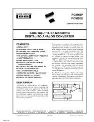
Ordering number : EN4624B<br />
CMOS IC<br />
<strong>LC78835K</strong>, <strong>78835KM</strong><br />
18 Bits Digital Filter and D/A Converter<br />
for Digital <strong>Audio</strong><br />
Overview<br />
The <strong>LC78835K</strong> and <strong>78835KM</strong> are 18-bit digital-to-analog<br />
D/A converter CMOS ICs with an on-chip eight-times<br />
oversampling digital filter. The LC78835 and the<br />
LC78835M are pin compatible.<br />
Features<br />
• Digital filter<br />
— 8 fs oversampling filter: 3-stage finite-impulseresponse<br />
(FIR) filter design (43rd-, 11th-, and thirdorders)<br />
— De-emphasis filter: Supports fs = 32 kHz, 44.1 kHz,<br />
or 48 kHz<br />
— Soft mute<br />
— Noise shaper<br />
— Supports double-rate sampling<br />
• D/A converter<br />
— Dynamic level-shifting 18-bit digital-to-analog<br />
converter<br />
— On-chip 2-channel D/A converter (with<br />
corresponding output)<br />
— On-chip output op-amp<br />
— Supports 384 fs, 392 fs, 448 fs, or 512 fs system<br />
clock<br />
— Single 5 V supply<br />
— Permits low-voltage operation (3.5 V)<br />
— Low-power silicon-gate CMOS process<br />
Package Dimensions<br />
unit: mm<br />
3092-DIP24W<br />
[<strong>LC78835K</strong>]<br />
unit: mm<br />
3155-MFP24<br />
[<strong>LC78835K</strong>M]<br />
SANYO: DIP24W<br />
SANYO: MFP24<br />
SANYO Electric Co.,Ltd. Semiconductor Bussiness Headquarters<br />
TOKYO OFFICE Tokyo Bldg., 1-10, 1 Chome, Ueno, Taito-ku, TOKYO, 110 JAPAN<br />
73696HA (OT)/N1094TH (OT)/82793JN No. 4624-1/14
<strong>LC78835K</strong>, <strong>78835KM</strong><br />
Specifications<br />
Absolute Maximum Ratings at Ta = 25°C, V SS = 0°C<br />
Parameter Symbol Conditions Ratings Unit<br />
Maximum supply voltage V DD max –0.3 to + 7.0 V<br />
Input voltage V IN –0.3 to V DD + 0.3 V<br />
Output voltage V OUT –0.3 to V DD + 0.3 V<br />
Operating temperature Topr –30 to + 75 °C<br />
Storage temperature Tstg –40 to + 125 °C<br />
Allowable Operating Ranges<br />
Parameter Symbol Conditions<br />
min<br />
Ratings<br />
typ max<br />
Unit<br />
Supply voltage V DD 3.5 5.0 5.5 V<br />
Reference voltage high Vref H V DD – 0.3 V DD V<br />
Reference voltage low Vref L 0 0.3 V<br />
Operating temperature Topr –30 +75 °C<br />
DC Characteristics at Ta = –30 to +75°C, V DD = 3.5 to 5.5 V, V SS = 0 V<br />
Ratings<br />
Parameter Symbol Conditions<br />
min typ max<br />
Unit<br />
Input high level voltage (1) V IH 1 3, 4, 5, 6, 7, 13, 14, 15, 16, 17 and 18 pin 2.2 V<br />
Input low level voltage (1) V IL 1 3, 4, 5, 6, 7, 13, 14, 15, 16, 17 and 18 pin 0.8 V<br />
Input high level voltage (2) V IH 2 11 pin 0.7V DD V<br />
Input low level voltage (2) V IL 2 11 pin 0.3V DD V<br />
Output high level voltage V OH 9 pin: I OH = –3 mA 2.4 V<br />
Output low level voltage V OL 9 pin: I OL = 3 mA 0.4 V<br />
Input leakage current I L *, V I = V SS , V DD –25 +25 µA<br />
Note: * 3, 4, 5, 6, 7, 11, 13, 14, 15, 16, 17 and 18 pin<br />
AC Characteristics at Ta = –30 to +75°C, V DD = 3.5 to 5.5 V, V SS = 0 V<br />
Parameter Symbol Conditions<br />
min<br />
Ratings<br />
typ max<br />
Unit<br />
Oscillation frequency f X XIN pin for crystal oscillator 1.0 25 MHz<br />
Clock pulse width t CW With external clock input to other than XIN pin 18 ns<br />
Clock pulse phase t CY With external clock input to other than XIN pin 40 1000 ns<br />
BCLK pulse width t BCW 60 ns<br />
BCLK pulse phase t BCY 120 ns<br />
Data setup time t DS 40 ns<br />
Data hold time t DH 40 ns<br />
LRCK setup time t LRS 40 ns<br />
LRCK hold time t LRH 40 ns<br />
No. 4624-2/14
<strong>LC78835K</strong>, <strong>78835KM</strong><br />
<strong>Audio</strong> Input Waveforms<br />
Electrical Characteristics (1)<br />
at Ta = 25°C, AV DD = DV DD = VrefH = 5.0 V, AGND = DGND = VrefL = 0 V, unless otherwise specified<br />
Parameter Symbol Conditions<br />
min<br />
Ratings<br />
typ max<br />
Unit<br />
D/A converter resolution RES 18 Bits<br />
Total harmonic distortion THD At 1 kHz, 0 dB *1 0.08 %<br />
Dynamic range DR At 1 kHz, –60 dB 90 dB<br />
Crosstalk CT At 1 kHz, 0 dB –85 dB<br />
Signal-to-noise ratio S/N JIS-A 96 dB<br />
Full-scale output voltage VFS 3.0 V P-P<br />
Power dissipation Pd *2 135 200 mW<br />
Output load resistance RL 21, 23 pin 5 kΩ<br />
Note: 1. “0 dB” signifies full scale.<br />
2. XIN pulse width (pin 11) 1.5 to 3.5 V, fx = 16.9344 MHz<br />
Test circuit: Based on application circuit<br />
No. 4624-3/14
<strong>LC78835K</strong>, <strong>78835KM</strong><br />
Electrical Characteristics (2)<br />
at Ta = 25°C, AV DD = DV DD = VrefH 3.5 V, AGND = DGND = VrefH = 0 V, unless otherwise specified<br />
Parameter Symbol Conditions<br />
min<br />
Ratings<br />
typ max<br />
Unit<br />
D/A converter resolution RES 18 Bits<br />
Total harmonic distortion THD At 1 kHz, 0dB *1 0.09 %<br />
Dynamic range DR At 1 kHz, –60 dB 90 dB<br />
Crosstalk CT At 1 kHz, 0 dB –85 dB<br />
Signal-to-noise ratio S/N JIS-A 96 dB<br />
Full-scale output voltage VFS 2.1 V P-P<br />
Power dissipation Pd *2 50 75 mW<br />
Output load resistance RL 21, 23 pin 15 kΩ<br />
Note: 1. “0 dB” signifies full scale.<br />
2. XIN pulse width (pin 11) 1.0 to 2.5 V, fx = 16.9344 MHz<br />
Test circuit: Based on application circuit<br />
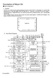
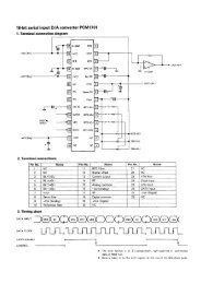
Block Diagram<br />
Pin Assignment<br />
No. 4624-4/14
<strong>LC78835K</strong>, <strong>78835KM</strong><br />
Pin Description<br />
Number Name Description<br />
1 REFH Reference voltage “H” pin<br />
Normally connected to AGND via a capacitor<br />
2 VrefH Reference voltage “H” input pin<br />
3 MUTE Mute signal input pin<br />
Soft mute is on when high<br />
4 D/N Normal/double-speed operation toggle<br />
Double-speed operation when high, normal operation when low<br />
5 BCLK Bit clock input pin<br />
6 DATA Digital audio data input pin<br />
2’s complement code, with input from the most significant bit (MSB)<br />
7 LRCK Left-right clock input pin<br />
Channel 1 when high, channel 2 when low<br />
8 DV DD Digital power supply pin<br />
9 CKOUT Clock output pin<br />
When at 392 fs: 196 fs clock<br />
When not at 392 fs: XIN-frequency clock<br />
10 XOUT Crystal oscillator output pin (system clock output pin)<br />
11 XIN Crystal oscillator input pin (system clock input pin)<br />
12 DGND Digital ground pin<br />
13 INITB Initialization signal input pin<br />
Initialization performed when low<br />
14 EMP On/Off toggle for the de-emphasis filter<br />
On when high, off when low<br />
15 FS1 32 kHz/44.1 kHz/48 kHz selector for the de-emphasis filter<br />
16 FS2<br />
FS1 L H H L<br />
FS2 L L H H<br />
fs 44.1 kHz 32 kHz 48 kHz<br />
17 CKSL1 System clock selector pin<br />
18 CKSL2<br />
CKSL1 CKSL2 System Clock<br />
L L 384 fs<br />
L H 392 fs<br />
H L 448 fs<br />
H H 512 fs<br />
19 VrefL Reference voltage “L” input pin<br />
20 REFL Reference voltage “L” pin<br />
Normally connected to AGND via a capacitor<br />
21 CH2OUT Channel 2 analog output pin<br />
22 AGND Analog ground pin<br />
23 CH1OUT Channel 1 analog output pin<br />
24 AV DD Analog power supply pin<br />
No. 4624-5/14
<strong>LC78835K</strong>, <strong>78835KM</strong><br />
Description of Operation<br />
1. Digital Filter<br />
The <strong>LC78835K</strong> and <strong>78835KM</strong> perform arithmetic functions as shown in the following block diagrams.<br />
• Oversampling<br />
Constructed of twice as many interpolation filters with a cascade connection arrangement using finite-impulseresponse<br />
(FIR) filters. When operating in normal-rate mode, data is transferred through a three-stage cascading<br />
process consisting of 43rd-order, 11th-order, and third-order finite impulse response (FIR) filters connected<br />
together to produce an eight-times oversampled signal. When operating in double-rate mode, data is transferred<br />
through a two-stage cascading process consisting of 43rd-order and second-order finite-impulse-response (FIR)<br />
connected filters to give a four-times oversampled signal. For further details concerning filter characteristics, refer<br />
to page 12.<br />
• De-emphasis<br />
Digital de-emphasis is performed using a first-order infinite-impulse-response (IIR) filter. Filter supported<br />
sampling frequencies include fs = 32 kHz, 44.1 kHz and 48 kHz (frequencies are all doubled with double-rate<br />
mode).<br />
No. 4624-6/14
For further details concerning filter characteristics when de-emphasis is on, refer to page 13.<br />
— De-emphasis on/off<br />
De-emphasis on: EMP pin = “H”<br />
De-emphasis off: EMP pin = “L”<br />
— Selection of filter coefficient<br />
<strong>LC78835K</strong>, <strong>78835KM</strong><br />
FS1 L H H L<br />
FS2 L L H H<br />
fs 44.1 kHz 32 kHz 48 kHz<br />
• Soft Mute<br />
Soft muting is performed using the built-in digital attenuator. The attenuation amount of the attenuator circuit is as<br />
follows:<br />
20 log (ATT/256) dB<br />
Although ATT = 0 to 256, when ATT = 0, attenuation sets to – ∞. If the MUTE pin is set to “H” level, ATT<br />
approaches 0 in single-decreasing increments and the attenuation changes towards – ∞. On the other hand, when<br />
the MUTE pin is set to the “L” level, ATT approaches 256 in single-increasing increments and the attenuation<br />
amount changes to approach 0. The approximate speed during soft mute is 1024/fs.<br />
• Noise Shaper<br />
In order to reduce noise during DF arithmetic output requantization, the first-order noise shaper is utilized.<br />
• Double-Rate Support<br />
When the D/N pin is set to “H” level, CD high-speed playback is supported. At this time, BCLK, LRCK and<br />
DATA are input at double the frequency of normal operating times. The system clock operates at 384 fs and with<br />
a clock speed of 512 fs, double-rate is supported. Note that test mode is enabled for clock speeds of 392 fs and<br />
448fs and double-rate is not supported.<br />
Normal-rate mode: D/N pin = “L”<br />
Double-rate mode: D/N pin = “H”<br />
No. 4624-7/14
<strong>LC78835K</strong>, <strong>78835KM</strong><br />
2. Initialization<br />
Initialization is necessary when power is applied or the system clock is replaced. When the INITB pin has been set<br />
to an “L” level, the supply to XIN, BCLK, and LRCK should be connected only after the supply has stabilized at the<br />
“L” level. As shown in the figure, a period greater than one LRCK cycle is required.<br />
When INITB = “L,” all 18-bit digital filter outputs set to 0, and the D/A converter’s output (CH1OUT, CH2OUT)<br />
equals 0 analog output (approximately (VREFH + VREFL)/2 electric potential).<br />
3. System Clock<br />
This IC supports four system clock speeds including 384 fs, 392 fs, 448 fs, and 512 fs. These may be selected using<br />
the CKSL1 and CKSL2 pins.<br />
CKSL1 CKSL2 System Clock<br />
L L 384 fs<br />
L H 392 fs<br />
H L 448 fs<br />
H H 512 fs<br />
• CKOUT Pin<br />
When operating at 392 fs, clock output is 196 fs or half that of the system clock. All other speeds result in clock<br />
output equal to that of the system.<br />
No. 4624-8/14
<strong>LC78835K</strong>, <strong>78835KM</strong><br />
4. Digital <strong>Audio</strong> Data Input<br />
Digital audio data supports MSB first and 2’s complement code using a 16-bit serial signal. 16-bit serial data is input<br />
from the DATA pin at the edge of BCLK rising and is input to the internal register along with readings at the rising and<br />
falling edges of LRCK.<br />
Digital <strong>Audio</strong> Data Input Timing<br />
No. 4624-9/14
<strong>LC78835K</strong>, <strong>78835KM</strong><br />
5. Digital-to-Analog (D/A) Converter<br />
These chips have built-in output operational amplifiers which use two independent on-chip D/A converters for CH1<br />
and CH2. Both use dynamic level shift, combining resistance strings (R-string D/A conversion), pulse-width<br />
modulation (PWM D/A conversion) and level shift D/A conversion modes. (See figure below.)<br />
• Resistance String (R-string) D/A Converter<br />
This 9-bit D/A converter circuit has 512 (=2 9 ) unit resistors (R) connected in series so that a potential applied to<br />
both ends is subjected to 512-way division. The two adjoining potentials V2 and V1 of the divided potentials<br />
corresponding to the values of the 9 MSBs of data (D15 to D9) are sent via a switching circuit to the PWM D/A<br />
converter. At this point, V2 – V1 = (VH – VL)/512.<br />
No. 4624-10/14
• Pulse-Width Modulation (PWM) D/A Converter<br />
This is a 3-bit circuit that applies pulse width modulation to voltages V2 and V1 output from the R-string D/A<br />
converter to produce an 8-way division. Depending on the value of the data in bits D8 to D6, one of the voltages,<br />
V2 or V1, is output to the CH1OUT (or CH2OUT) pin.<br />
• Level Shift D/A Converter<br />
The variable resistors VRH and VRL are connected in series to the two ends of the R-string D/A converter<br />
resistance, configuring a 6-bit D/A conversion circuit. Depending on the values of the data in the LSBs (bits D5 to<br />
D0), VRH and VRL change as follows.<br />
(1) The sum of VRH and VRL is constant, irrespective of the data value.<br />
(2) Irrespective of the data value, VRH and VRL are in the range of 0 to 63R/512 (where R is the unit resistance of<br />
the R-string D/A converter) and resistance changes in R/512 steps in accordance with the data value.<br />
This means that the R-string D/A converter outputs, V2 and V1, each vary in the range of 0 to 63 × ∆V/512 (∆V =<br />
(VH - VL)/512) in ∆V/512 steps.<br />
— Vref H/L, REF H/L Pins<br />
<strong>LC78835K</strong>, <strong>78835KM</strong><br />
The voltage on the Vref pins, used to apply the reference voltage to the resistance strings, are usually set so that<br />
VrefH = AV DD and VrefL = AGND. In addition, a 10 µF rated condenser connects REFH and AGND as well<br />
as REFL and AGND. When VrefH = 5.0 V, VrefL = 0 V, the <strong>LC78835K</strong> on-chip RH and RL resistors<br />
maximum output amplitude at 0 dB playback is output in the 3.0 Vp-p range extending from a minimum 0.6 V<br />
to maximum 3.6 V.<br />
No. 4624-11/14
<strong>LC78835K</strong>, <strong>78835KM</strong><br />
Filter Characteristics (theoretical values)<br />
Normal-rate mode: 8 fs oversampling<br />
Double-rate mode: 4 fs oversampling<br />
Ripple:<br />
within ±0.05 dB<br />
Attenuation amount: –40 dB or less<br />
•Normal Rate (De-emphasis Off)<br />
•Double Rate (De-emphasis Off)<br />
No. 4624-12/14
<strong>LC78835K</strong>, <strong>78835KM</strong><br />
Pass Band Characteristics with De-emphasis On<br />
• Normal Rate • Double Rate<br />
Sample Application Circuit<br />
Note: 1. Within the sample application circuit, DV DD connects to DGND as the digital ground, and AV DD connects to<br />
AGND as the analog ground.<br />
2. For AV DD and VrefH, a low-impedance high-stability power supply (commercially available 3-pin regulator or<br />
compatible) should be used.<br />
3. If 8-pin (DV DD ) and 24-pin (AV DD ) rise timings deviate, latch-up may occur. For this reason, no difference<br />
should exist between 8 and 24 pin power application timing.<br />
4.A clock signal must be supplied to the XIN pin immediately after power is applied. The IC may be destroyed if<br />
the XIN pin is held either high or low when power is applied.<br />
No. 4624-13/14
<strong>LC78835K</strong>, <strong>78835KM</strong><br />
■ No products described or contained herein are intended for use in surgical implants, life-support systems, aerospace<br />
equipment, nuclear power control systems, vehicles, disaster/crime-prevention equipment and the like, the failure of<br />
which may directly or indirectly cause injury, death or property loss.<br />
■ Anyone purchasing any products described or contained herein for an above-mentioned use shall:<br />
1 Accept full responsibility and indemnify and defend SANYO ELECTRIC CO., LTD., its affiliates, subsidiaries and<br />
distributors and all their officers and employees, jointly and severally, against any and all claims and litigation and all<br />
damages, cost and expenses associated with such use:<br />
➁ Not impose any responsibility for any fault or negligence which may be cited in any such claim or litigation on<br />
SANYO ELECTRIC CO., LTD., its affiliates, subsidiaries and distributors or any of their officers and employees<br />
jointly or severally.<br />
■ Information (including circuit diagrams and circuit parameters) herein is for example only; it is not guaranteed for<br />
volume production. SANYO believes information herein is accurate and reliable, but no guarantees are made or implied<br />
regarding its use or any infringements of intellectual property rights or other rights of third parties.<br />
This catalog provides information as of July, 1996. Specifications and information herein are subject to change<br />
without notice.<br />
No. 4624-14/14