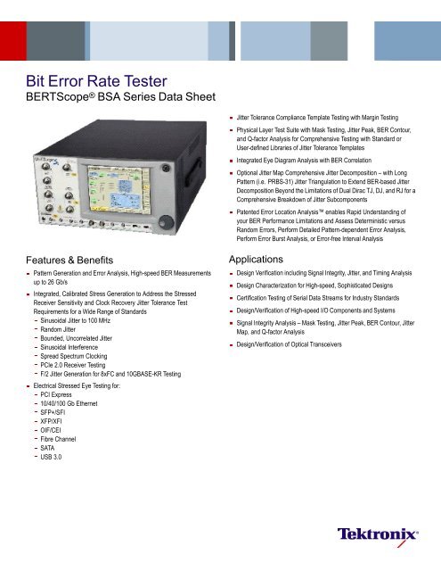
Bit Error Rate Tester - BERTScope® BSA Series - Nortelco
Bit Error Rate Tester - BERTScope® BSA Series - Nortelco
Bit Error Rate Tester - BERTScope® BSA Series - Nortelco

You also want an ePaper? Increase the reach of your titles
YUMPU automatically turns print PDFs into web optimized ePapers that Google loves.
<strong>Bit</strong> <strong>Error</strong> <strong>Rate</strong> <strong>Tester</strong><br />
BERTScope ® <strong>BSA</strong> <strong>Series</strong> Data Sheet<br />
Jitter Tolerance Compliance Template Testing with Margin Testing<br />
Physical Layer Test Suite with Mask Testing, Jitter Peak, BER Contour,<br />
and Q-factor Analysis for Comprehensive Testing with Standard or<br />
User-defined Libraries of Jitter Tolerance Templates<br />
Integrated Eye Diagram Analysis with BER Correlation<br />
Optional Jitter Map Comprehensive Jitter Decomposition – with Long<br />
Pattern (i.e. PRBS-31) Jitter Triangulation to Extend BER-based Jitter<br />
Decomposition Beyond the Limitations of Dual Dirac TJ, DJ, and RJ for a<br />
Comprehensive Breakdown of Jitter Subcomponents<br />
Patented <strong>Error</strong> Location Analysis enables Rapid Understanding of<br />
your BER Performance Limitations and Assess Deterministic versus<br />
Random <strong>Error</strong>s, Perform Detailed Pattern-dependent <strong>Error</strong> Analysis,<br />
Perform <strong>Error</strong> Burst Analysis, or <strong>Error</strong>-free Interval Analysis<br />
Features & Benefits<br />
Pattern Generation and <strong>Error</strong> Analysis, High-speed BER Measurements<br />
up to 26 Gb/s<br />
Integrated, Calibrated Stress Generation to Address the Stressed<br />
Receiver Sensitivity and Clock Recovery Jitter Tolerance Test<br />
Requirements for a Wide Range of Standards<br />
Sinusoidal Jitter to 100 MHz<br />
Random Jitter<br />
Bounded, Uncorrelated Jitter<br />
Sinusoidal Interference<br />
Spread Spectrum Clocking<br />
PCIe 2.0 Receiver Testing<br />
F/2 Jitter Generation for 8xFC and 10GBASE-KR Testing<br />
Electrical Stressed Eye Testing for:<br />
PCI Express<br />
10/40/100 Gb Ethernet<br />
SFP+/SFI<br />
XFP/XFI<br />
OIF/CEI<br />
Fibre Channel<br />
SATA<br />
USB 3.0<br />
Applications<br />
Design Verification including Signal Integrity, Jitter, and Timing Analysis<br />
Design Characterization for High-speed, Sophisticated Designs<br />
Certification Testing of Serial Data Streams for Industry Standards<br />
Design/Verification of High-speed I/O Components and Systems<br />
Signal Integrity Analysis – Mask Testing, Jitter Peak, BER Contour, Jitter<br />
Map, and Q-factor Analysis<br />
Design/Verification of Optical Transceivers
Data Sheet<br />
Linking Domains<br />
Eye diagrams have always provided an easy and intuitive view of digital<br />
performance. It has been harder to tie this directly with BER performance,<br />
as the instruments that provide views of each have been architected in<br />
fundamentally different ways. Eye diagrams have been composed of<br />
shallow amounts of data that have not easily uncovered rarer events.<br />
BERTs have counted every bit and so have provided measurements based<br />
on vastly deeper data sets, but have lacked the intuitive presentation of<br />
information to aid troubleshooting.<br />
The BERTScope removes this gap allowing you to quickly and easily view<br />
an eye diagram based on at least two orders of magnitude more data than<br />
conventional eyes. Seeing a feature that looks out of the ordinary, you<br />
are able to place cursors on the item of interest and by simply moving the<br />
sampling point of the BERT, use the powerful error analysis capabilities<br />
to gain more insight into the feature of interest. For example, check for<br />
pattern sensitivity of the latest rising edges. Alternatively, use one-button<br />
measurement of BER Contour to see whether performance issues are<br />
bounded or likely to cause critical failures in the field. In each case,<br />
information is readily available to enhance modeling or aid troubleshooting,<br />
and is available for patterns up to 2 31 –1PRBS.<br />
Data-rich Eye Diagrams<br />
As shown previously, there is an impressive difference in data depth<br />
between conventional eye diagrams and those taken with a BERTScope.<br />
So what does that mean? It means that you see more of what is really<br />
going on – more of the world of low-probability events that is present every<br />
time you run a long pattern through a dispersive system of any kind, have<br />
Testing optical transmitters with BERTScope mask testing and a BERTScope CR.<br />
The BERTScope shown with optical units enabled. In this example measurements are<br />
converted to the optical domain automatically.<br />
random noise or random jitter from a VCO – a world that is waiting to catch<br />
you out when your design is deployed. Adding to this the deeper knowledge<br />
that comes from the one-button measurements of BER Contour, Jitter Peak,<br />
and Q-factor, and you can be confident that you are seeing the complete<br />
picture.<br />
2 www.tektronix.com
<strong>Bit</strong> <strong>Error</strong> <strong>Rate</strong> <strong>Tester</strong> — BERTScope ® <strong>BSA</strong> <strong>Series</strong><br />
Clock path in BERTScope Option STR models.<br />
With the ability to vary sample depth, it is very easy to move between deep measurements<br />
which give a more accurate view of the real system performance, and shallow<br />
measurements that match those of a sampling scope. The measurements shown here<br />
are from the eye diagram of an optical transmitter. With the BERTScope sample depth<br />
set to only 3000 waveforms, the BERTScope generates the diagram shown in the middle<br />
in only 1 second. The measured mask margin of 20% exactly correlates to the same<br />
measurement made on a sampling oscilloscope. The lower diagram shows the eye<br />
produced by the same device, using Compliance Contour measured at a BER of 1×10 –6 .<br />
Here the mask margin is reduced to 17%.<br />
Deep Mask Testing<br />
The depth advantage gained for eye diagrams is at least 10 times greater<br />
for mask testing. Unlike pseudo-mask testing offered by some BERTs,<br />
a BERTScope mask test samples every point on the perimeter of an<br />
industry-standard mask, including the regions above and below the eye. Not<br />
only that, but each point is tested to a depth unseen before. This means<br />
that even for a test lasting a few seconds using a mask from the library of<br />
standard masks or from a mask you have created yourself, you can be sure<br />
that your device has no lurking problems.<br />
Accurate Jitter Testing to Industry Standards<br />
Testing with long or short patterns, the most accurate jitter measurement is<br />
likely to come from the methodology that uses little or no extrapolation to<br />
get its result. With the BERTScope, you can quickly measure to levels of<br />
1×10 –9 (1×10 –10 at high data rates), or wait for the instrument to measure<br />
1×10 –12 directly. Either way, the BERTScope’s one-button measurements<br />
are compliant to the MJSQ jitter methodology, and because the underlying<br />
delay control is the best available on any BERT you can be sure that the<br />
measurements are accurate. Use the built-in calculations for Total Jitter<br />
(TJ), Random Jitter (RJ), and Deterministic Jitter (DJ), or easily export the<br />
data and use your own favorite jitter model.<br />
Mask Compliance Contour Testing<br />
Many standards such as XFP/XFI and OIF CEI now specify mask tests<br />
intended to assure a specified 1×10 –12 eye opening. Compliance Contour<br />
view makes this easy by taking a mask, and overlaying it on your measured<br />
BER contours – so you can immediately see whether you have passed the<br />
mask at whatever BER level you decide.<br />
Quick Selection Guide<br />
Model Max <strong>Bit</strong> <strong>Rate</strong> Stressed Eye – Generator/Analyzer<br />
SJ, RJ, BUJ, SI<br />
<strong>BSA</strong>260C/CPG 26 Gb/s Opt. STR Both<br />
<strong>BSA</strong>175C/CPG 17.5 Gb/s Opt. STR Both<br />
<strong>BSA</strong>125C/CPG 12.5 Gb/s Opt. STR Both<br />
<strong>BSA</strong>85C/CPG 8.5 Gb/s Opt. STR Both<br />
Flexible Clocking<br />
The generator clock path features in the BERTScope provides the test<br />
flexibility needed for emerging real-world devices. Whether computer cards<br />
or disk drives, it is often necessary to be able to provide a sub-rate system<br />
clock, such as 100 MHz for PCI Express ® (PCIe). To get the target card<br />
running may require a differential clock signal with a particular amplitude<br />
and offset; this is easily accomplished with the BERTScope architecture,<br />
with many flexible divide ratios available.<br />
Spread Spectrum Clocking (SSC) is commonly used in electrical serial<br />
data systems to reduce EMI energy by dispersing the power spectrum.<br />
Adjustable modulation amplitude, frequency, and a choice of triangle or sine<br />
modulation wave shape allow testing receivers to any compliance standard<br />
which utilize SSC. An additional modulator and source allows users to<br />
stress the clock with high-amplitude, low-frequency Sinusoidal Jitter (SJ).<br />
www.tektronix.com 3
Data Sheet<br />
In keeping with the BERTScope philosophy, the graphical user interface presents the<br />
control functionality in a logical, easy-to-follow format. A time domain representation of<br />
the response shows the effects of tap weight settings. The frequency domain Bode plot<br />
shows how the filter will compensate for the channel losses.<br />
PatternVu<br />
WorkingwithClosedEyes<br />
With the need to push ever-increasing data rates through electrical<br />
channels, the frequency-dependent losses often result in eye closure at the<br />
receiver end. Engineers use equalization to compensate for these losses<br />
and “open the eyes” in the real system. Tektronix offers powerful tools<br />
that allow designers to characterize and test compliance of receiver and<br />
transmitter components used in these systems.<br />
For receiver testing, the DPP125 Digital Pre-emphasis Processor adds<br />
calibrated pre-emphasis to the BERTScope pattern generator outputs,<br />
emulating pre-emphasis applied at the transmitter. Pre-emphasis is<br />
currently used in 10GBASE-KR, PCIe, SAS, DisplayPort ® , USB 3.0, and<br />
other standards.<br />
Features:<br />
1-12.5 Gb/s clock rates<br />
3- or 4-tap versions<br />
Flexible cursor placement allowing pre-cursor or post-cursor<br />
PatternVu<br />
The PatternVu option includes a software-implemented FIR filter which can<br />
be inserted before the eye pattern display. In systems employing receiver<br />
equalization, this allows you to view the eye diagram and perform physical<br />
measurements on the eye as the receiver’s detector would see it, after the<br />
effect of the equalizer. Equalizers with up to 32 taps can be implemented,<br />
and the user can select the tap resolution per UI.<br />
PatternVu also includes CleanEye, a pattern-locked averaging system<br />
which removes the nondeterministic jitter components from the eye.<br />
This allows you to clearly see pattern-dependent effects such as ISI<br />
The intuitive user interface provides easy control of all operating parameters. A unique<br />
Loop Response view shows the loop characteristics – actually measured, not just the<br />
settings value.<br />
(Inter-Symbol Interference) which are normally obscured by the presence of<br />
high amounts of random jitter.<br />
Single Value Waveform export is a component in the PatternVu option.<br />
This allows you to capture a pattern-locked waveform showing single bits,<br />
similar to a single-shot capture in a real-time oscilloscope. Once captured,<br />
the waveform can be exported in a variety of formats for further analysis in<br />
an external program.<br />
Add Clock Recovery<br />
The Tektronix CR125A, CR175A, and CR286A add new levels of flexibility<br />
in compliant clock recovery. Most standards requiring jitter measurement<br />
specify the use of clock recovery, and exactly which loop bandwidth must<br />
be used. Using a different or unknown loop bandwidth will almost certainly<br />
give you the wrong jitter measurement. The new clock recovery instrument<br />
enables easy and accurate measurements to be made to all of the common<br />
standards.<br />
4 www.tektronix.com
<strong>Bit</strong> <strong>Error</strong> <strong>Rate</strong> <strong>Tester</strong> — BERTScope ® <strong>BSA</strong> <strong>Series</strong><br />
SSC Waveform Measurement<br />
The usefulness of the BERTScope CRs is not just confined to BERTScope<br />
measurements. Use them stand-alone in the lab with your sampling oscilloscopes, or with<br />
existing BERT equipment. Compliant measurements are available to you by pairing either<br />
of these versatile instruments with your existing investments.<br />
Display and Measure SSC Modulation<br />
Waveforms<br />
Spread Spectrum Clocking (SSC) is used by many of the latest serial<br />
busses including SATA, PCI Express, and next-generation SAS in order<br />
to reduce EMI issues in new board and system designs. The Tektronix<br />
CR Family provides spread spectrum clock recovery together with the<br />
display and measurement of the SSC modulation waveform. Automated<br />
measurements include minimum and maximum frequency deviation (in ppm<br />
or ps), modulation rate of change (dF/dT), and modulation frequency. Also<br />
included are display of the nominal data frequency and easy-to-use vertical<br />
and horizontal cursors.<br />
Add Jitter Analysis<br />
Combine a Tektronix CR125A, CR175A, or CR286A with Option GJ with<br />
your sampling scope or BERTScope for variable clock recovery from 1.2 to<br />
11.2 Gb/s, Duty Cycle Distortion (DCD) measurement, and real-time jitter<br />
spectral analysis. Display jitter spectral components from 200 Hz to 90 MHz<br />
with cursor measurements of jitter and frequency. Measure band-limited<br />
integrated jitter with user-settable frequency-gated measurements (preset<br />
Jitter Spectrum Measurement<br />
band limits and integrated jitter measurement for PCI Express 2.0 jitter<br />
spectrum in this example).<br />
www.tektronix.com 5
Data Sheet<br />
Creating the stress recipe for receiver testing to a complicated standard such as PCIe<br />
2.0 used to require "racking and stacking" several instruments, then spending hours<br />
calibrating the setup. With BERTScope, an easy-to-understand graphical view gives you<br />
control of all of the calibrated stress sources you need – inside the same instrument.<br />
Eliminating the need for external cabling, mixers, couplers, modulators, etc. simplifies<br />
stress calibration.<br />
Taking the Stress out of Receiver Testing<br />
As networks have changed, so have the challenges of testing receivers.<br />
While tests such as BER and receiver sensitivity are still important, receiver<br />
jitter tolerance has evolved to be more real-world for jitter-limited systems<br />
such as 10 Gb/s data over back planes and new high-speed buses.<br />
Stressed Eye testing is becoming increasingly common as a compliance<br />
measurement in many standards. In addition, engineers are using it to<br />
explore the limits of their receiver performance to check margins in design<br />
and manufacturing.<br />
Flexible Stress Impairments<br />
Flexible Stress Impairments<br />
The BERTScope has high-quality, calibrated sources of stress built-in,<br />
including RJ, SJ, BUJ, and SI.<br />
ISI is also a common ingredient in many standards. The <strong>BSA</strong>12500ISI<br />
differential ISI board provides a wide variety of path lengths, free from<br />
switching suck-outs and anomalies.<br />
Many standards call for SJ to be stepped through a template with different SJ amplitudes<br />
at particular modulation frequencies. This is easy with the built-in Jitter Tolerance function<br />
which automatically steps through a template that you designed, or one of the many<br />
standard templates in the library.<br />
6 www.tektronix.com
<strong>Bit</strong> <strong>Error</strong> <strong>Rate</strong> <strong>Tester</strong> — BERTScope ® <strong>BSA</strong> <strong>Series</strong><br />
Pattern Capture<br />
Stressed Eye Option<br />
Using the Power of <strong>Error</strong> Analysis – In this example eye diagram views were linked with<br />
BER to identify and solve a design issue in a memory chip controller. The eye diagram<br />
(top left) shows a feature in the crossing region that is unexpected and appearing less<br />
frequently than the main eye. Moving the BER decision point to explore the infrequent<br />
events is revealing. <strong>Error</strong> Analysis shows that the features are related in some way to the<br />
number 24. Further investigation traced the anomaly to clock breakthrough within the IC;<br />
the system clock was at 1/24th of the output data rate. Redesigning the chip with greater<br />
clock path isolation gave the clean waveform of the top right eye diagram.<br />
Uses include receiver testing of devices with internal BER measurement<br />
ability such as DisplayPort, or adding stress capability to legacy BERT<br />
instruments.<br />
BERTScope Pattern Generator<br />
BERTScope Pattern Generator Family<br />
The <strong>BSA</strong>125CPG, <strong>BSA</strong>175CPG, and <strong>BSA</strong>260CPG Family of pattern<br />
generators provide a full range of PRBS patterns, common standards-based<br />
patterns, and user-defined patterns. Option STR provides full integrated,<br />
calibrated stress generation which is an easy-to-use alternative to a rack full<br />
of manually calibrated instruments needed to provide a stressed pattern.<br />
Pattern Capture<br />
There are several methods for dealing with unknown incoming data. In<br />
addition to Live Data Analysis discussed above, a useful standard feature<br />
on all BERTScope analyzers is pattern capture. This allows the user to<br />
specify the length of a repeating pattern and then allow the analyzer to grab<br />
the specified incoming data using the detector’s 128 Mb RAM memory. This<br />
can then be used as the new detector reference pattern, or edited and<br />
saved for later use.<br />
www.tektronix.com 7
Data Sheet<br />
MJSQ-compliant Dual Dirac jitter measurement.<br />
Jitter Peak and BER Contour measurements made on live data.<br />
Jitter Map<br />
Jitter Measurements<br />
Multi-gigabit serial data channels have eye openings only a couple hundred<br />
picoseconds wide – or less. In systems where only a few picoseconds of<br />
jitter count, accurate measurement of jitter is essential for managing tight<br />
jitter budgets. The BERTScope has two sets of tools which perform these<br />
critical measurements.<br />
The Physical Layer Test Suite option includes measurement of Total Jitter<br />
(TJ) along with breakdown into Random Jitter (RJ) and Deterministic<br />
Jitter (DJ), using the well-accepted Dual Dirac method. The deep,<br />
BERT-collected measurements use several orders of magnitude less<br />
extrapolation, or in some cases no extrapolation, than oscilloscopes use as<br />
a basis for the jitter measurements. This produces inherently more accurate<br />
results than measurements made on other instruments which rely on high<br />
levels of extrapolation.<br />
The optional Jitter Map is the latest suite of jitter measurements available<br />
for the BERTScope. It provides a comprehensive set of subcomponent<br />
analysis beyond RJ and DJ, including many measurements compliant with<br />
higher data rate standards. Jitter Map can also measure and decompose<br />
jitter on extremely long patterns, such as PRBS-31, as well as live data<br />
(requires Live Data Analysis option) providing that it can first run on a<br />
shorter synchronized data pattern.<br />
Features include:<br />
DJ breakdown into Bounded Uncorrelated Jitter (BUJ), Data Dependent<br />
Jitter (DDJ), Inter-Symbol Interference (ISI), Duty Cycle Distortion<br />
(DCD), and Sub-<strong>Rate</strong> Jitter (SRJ) including F/2 (or F2) Jitter<br />
BER-based for direct (non-extrapolated) Total Jitter (TJ) measurement<br />
to 10 –12 BER and beyond<br />
Separation of correlated and non-correlated jitter components eliminates<br />
mistaking long pattern DDJ for RJ<br />
Can measure jitter with minimum eye opening<br />
Additional levels of breakdown not available from other instruments such<br />
as: Emphasis Jitter (EJ), Uncorrelated Jitter (UJ), Data Dependent Pulse<br />
Width Shrinkage (DDPWS), and Non-ISI<br />
Intuitive, easy-to-navigate jitter tree<br />
Testing Interface Cards<br />
Finally a solution to the age-old problem of making physical layer<br />
measurements on high-speed line cards, motherboards, and live traffic<br />
– the BERTScope Live Data Analysis option. Through novel use of the<br />
dual-decision point architecture, the instrument is able to make parametric<br />
measurements such as Jitter, BER Contour, and Q-factor in addition to<br />
the eye and mask measurements that are usable as standard – all that is<br />
required is a clock signal. Add the Jitter Map option to see even more layers<br />
of jitter decomposition on live data. No more frustration because the pattern<br />
is not known, is unpredictable, or involves rate-matching word insertions.<br />
Troubleshooting is so much easier now that the one-button physical layer<br />
tests can be employed to provide unique insight.<br />
8 www.tektronix.com
<strong>Bit</strong> <strong>Error</strong> <strong>Rate</strong> <strong>Tester</strong> — BERTScope ® <strong>BSA</strong> <strong>Series</strong><br />
Figure 1. Amplitude range.<br />
Characteristics<br />
Pattern Generator* 1<br />
Input/Output Specifications<br />
Clock Outputs<br />
Characteristic<br />
Description<br />
Frequency Range<br />
<strong>BSA</strong>85C, CPG<br />
0.1-8.5 GHz<br />
<strong>BSA</strong>125C, CPG 0.1-12.5 GHz* 2<br />
<strong>BSA</strong>175C, CPG 0.5-17.5 GHz* 2<br />
<strong>BSA</strong>260C, CPG 1-26 GHz* 2<br />
Phase Noise<br />
< –90 dBc/Hz at 10 kHz offset (typical)<br />
Clock Output Divide Ratios Option STR only<br />
* 1 Rise times are measured 20% to 80% unless otherwise stated. Specifications are following a 20-minute<br />
warm-up period. Specifications subject to change.<br />
* 2 Output at data rate ÷2 above 11.2 Gb/s.<br />
Data Outputs<br />
Characteristic<br />
Description<br />
Date <strong>Rate</strong> Range<br />
<strong>BSA</strong>85C<br />
0.1-8.5 Gb/s<br />
<strong>BSA</strong>125C, CPG<br />
0.1-12.5 Gb/s<br />
<strong>BSA</strong>175C, CPG<br />
0.5-17.5 Gb/s<br />
<strong>BSA</strong>260C, CPG<br />
1-26 Gb/s<br />
Format<br />
NRZ<br />
Polarity<br />
Normal or Inverted<br />
Variable Crossover 25 to 75%<br />
Patterns<br />
Hardware patterns Industry-standard Pseudo-random (PRBS) of the<br />
following types: 2 n – 1 where n = 7, 11, 15, 20, 23,<br />
31<br />
RAM patterns<br />
<strong>BSA</strong>85C<br />
<strong>BSA</strong>125C, CPG<br />
<strong>BSA</strong>175C, CPG<br />
<strong>BSA</strong>260C, CPG<br />
Library<br />
<strong>Error</strong> Insertion<br />
Length<br />
Frequency<br />
128bitsto128Mbtotal,allocatedin32Mbportions<br />
to each of two A/B pages. Single page max is<br />
128 Mb<br />
Wide variety including SONET/SDH, Fibre Channel<br />
basedsuchask28.5,CJTPAT;2 n patterns where n<br />
=3,4,5,6,7,9;MarkDensitypatternsfor2 n where<br />
n = 7, 9, 23; and many more<br />
1,2,4,8,16,32,64bitbursts<br />
Single or repetitive<br />
Figure 2. Allowable combinations of termination and offset. Amplitude swings between<br />
0.25 and 2 V allowed; should fit inside shaded area of graph. For example, SCFL uses a<br />
0 V termination, and operates between approximately 0 and –0.9 V; as shown with dotted<br />
arrow, it falls within the operating range.<br />
Data, Clock Amplitudes and Offsets<br />
Characteristic<br />
Configuration<br />
Interface<br />
Preset Logic Families<br />
Terminations<br />
Allowable Amplitudes,<br />
Terminations, and Offsets<br />
Data, Clock Waveform Performance<br />
Description<br />
Differential outputs, each side of pair individually<br />
settable for termination, amplitude, offset<br />
DC coupled, 50 Ω reverse terminated, APC-3.5<br />
connector. Calibration into 75 Ω selectable, other<br />
impedances by keypad entry. User-replaceable<br />
Planar Crown ® adapter allows change to other<br />
connector types<br />
LVPECL,LVDS,LVTTL,CML,ECL,SCFL<br />
Variable, –2 to +2 V<br />
Presets: +1.5, +1.3, +1, 0, –2 V, AC coupled<br />
SeeFigures1and2<br />
Model Rise Time Jitter<br />
<strong>BSA</strong>85C<br />
<strong>BSA</strong>125C, CPG<br />
<strong>BSA</strong>175C, CPG<br />
<strong>BSA</strong>260C, CPG<br />
Clock/Data Delay<br />
Characteristic<br />
Range<br />
Up to 1.1 GHz<br />
Above 1.1 GHz<br />
Resolution<br />
Self Calibration<br />
25 ps max, 23 ps typical<br />
(10-90%)<br />
Description<br />
Data Sheet<br />
Pattern Generator Ancillary Connections<br />
Front-panel Pattern Generator Connections<br />
External Clock Input<br />
Characteristic<br />
Description<br />
Allows use of an external clock source to clock the BERTScope.<br />
Models equipped with stress are able to add impairments to incoming clock,<br />
including when external signal has Spread Spectrum Clocking (SSC) in excess of<br />
5000 ppm imposed on it.<br />
Frequency Range<br />
<strong>BSA</strong>85C<br />
0.1 to 8.5 GHz<br />
<strong>BSA</strong>125C, CPG<br />
0.1 to 12.5 GHz<br />
<strong>BSA</strong>175C, CPG<br />
0.5 to 17.5 GHz<br />
<strong>BSA</strong>260C, CPG<br />
1 to 26 GHz<br />
Nominal Power<br />
900 mV p-p (+3 dBm)<br />
Maximum Power<br />
2.0 V p-p (+10 dBm)<br />
Return Loss<br />
Better than –6 dB<br />
Interface<br />
50 Ω SMA female, DC coupled into selectable<br />
termination voltage<br />
HF Jitter (Option STR Only)<br />
Characteristic<br />
Description<br />
One of two jitter insertion inputs. Can be used to insert SJ, RJ, BUJ if desired.<br />
Frequency Range<br />
DC to 1.0 GHz<br />
Jitter Amplitude Range Up to 0.5 UI max<br />
Input Voltage Range<br />
0-2 V p-p (+10 dBm) for normal operation<br />
6.3 V p-p (+20 dBm) max nondestructive input<br />
Data <strong>Rate</strong> Range<br />
Up to 8.5, 11.2 (<strong>BSA</strong>125C, CPG, only), 17.5, or<br />
22 Gb/s<br />
Interface<br />
SMA female, 50 Ω, DC coupled into 0 V<br />
Sub-rate Clock Output<br />
Characteristic<br />
Description<br />
BERTScope standard models have clock divided by 4.<br />
BERTScope Option STR models have additional capabilities.<br />
Frequency Range<br />
0.125 to 3.125 GHz (12.5 GHz with Option STR)<br />
Amplitude Range<br />
1 V p-p , nominal, centered around 0 V<br />
Transition Time<br />
1 kΩ impedance into 0 V<br />
Sinusoidal Interference Output (Option STR Only)<br />
Characteristic<br />
Description<br />
SI output from internal generator. Can be used to apply SI after external ISI<br />
channel.<br />
Frequency Range<br />
0.1-2.5 GHz<br />
Output Voltage<br />
0-3 V p-p<br />
Interface<br />
0-3 V p-p<br />
Low-frequency Jitter Input (Option STR Only)<br />
Characteristic<br />
Description<br />
Allows use of external low-frequency jitter source to modulate the stressed pattern<br />
generator output.<br />
Frequency Range<br />
DC to 100 MHz<br />
Jitter Amplitude Range Up to 1.1 ns, can be combined with other internal<br />
low-frequency modulation<br />
Input Voltage Range<br />
0-2 V p-p (+10 dBm) for normal operation 6.3 V p-p<br />
(+20 dBm) max nondestructive input<br />
Data <strong>Rate</strong> Range<br />
Up to 8.5 Gb/s (<strong>BSA</strong>85C/CPG), 12.5 Gb/s<br />
(<strong>BSA</strong>125C/CPG), 17.5 Gb/s (<strong>BSA</strong>175C/CPG), and<br />
22 Gb/s (<strong>BSA</strong>260C/CPG)<br />
Interface<br />
SMA female 50 Ω, DC coupled into 0 V<br />
Low-frequency Sinusoidal Jitter Output<br />
(Option STR Only)<br />
Characteristic<br />
Description<br />
To allow phasing of two BERTScopes together, in-phase or anti-phase.<br />
Frequency<br />
As set for internal SJ from GUI<br />
Amplitude<br />
2 V p-p ,centeredat0V<br />
Interface<br />
SMA female<br />
10 www.tektronix.com
<strong>Bit</strong> <strong>Error</strong> <strong>Rate</strong> <strong>Tester</strong> — BERTScope ® <strong>BSA</strong> <strong>Series</strong><br />
Reference Input<br />
Characteristic<br />
Description<br />
To lock the BERTScope to an external frequency reference from of another piece<br />
of equipment.<br />
Frequency<br />
10, 100, 106.25, 133.33, 156.25, 166.67, or<br />
200 MHz<br />
Amplitude<br />
0.325 to 1.25 V p-p (–6to+6dBm)<br />
Interface<br />
50 Ω SMA female, AC coupled<br />
Reference Output<br />
Characteristic<br />
Description<br />
Provides a frequency reference for other instruments to lock to.<br />
Configuration<br />
Single Ended (Ref-Out not used) (<strong>BSA</strong>125C, CPG)<br />
Differential<br />
Frequency<br />
10, 100, 106.25, 133.33, 156.25, 166.67, or<br />
200 MHz<br />
Amplitude<br />
1V p-p (+4 dBm) nominal, each output, (2 V p-p<br />
differential)<br />
Interface<br />
50 Ω SMA female, AC coupled<br />
Available divide ratios from clock-related output, by bit rate, using the internal clock,<br />
<strong>BSA</strong>85C***.<br />
<strong>BSA</strong>125C, CPG, <strong>BSA</strong>175C, CPG, and <strong>BSA</strong>260C, CPG<br />
Clock Path Details<br />
<strong>BSA</strong>85C, CPG<br />
Functional block diagram of the clock path for models with stress capability,<br />
<strong>BSA</strong>85C/CPG, <strong>BSA</strong>125C/CPG, <strong>BSA</strong>175C/CPG, <strong>BSA</strong>260C/CPG.<br />
*Thisoutput can also provide a full-rate jittered clock.<br />
** Stress may be added to an external clock on appropriate models. Stress operating range is from 1.5 to<br />
11.2 Gb/s. External clock must have a duty cycle of 50% ±2%.<br />
*** All listed ratios available for an external clock input over entire bit rate range, limitations for internal<br />
clock only. Minimum specified frequency of the clock output is 100 MHz. Operation below this rate will<br />
be uncalibrated.<br />
Functional block diagram of the clock path for models with stress capability,<br />
<strong>BSA</strong>85C/CPG.<br />
The <strong>BSA</strong>125, <strong>BSA</strong>175, and <strong>BSA</strong>260 models use an internal Double Data <strong>Rate</strong><br />
(DDR) architecture to operate at data rates ≥11.2 Gb/s. When operating at 11.2 Gb/s<br />
or higher data rate, the clock output will be 1/2 the data rate.<br />
External clock can be specified to be either full or half data rate. When full rate is<br />
selected, the pattern generator will operate in DDR mode when the input clock<br />
frequency is 11.2 GHz or higher.<br />
These ratios apply to operation from internal clock only. External clock will be output<br />
at 1/2 rate when half rate is selected, or when full rate is selected and clock rate<br />
is ≥11.2 GHz.<br />
The minimum data rate specified for the main clock output is 500 Mb/s. Output will be<br />
uncalibrated when operated at divided rates lower than 500 Mb/s.<br />
www.tektronix.com 11
Data Sheet<br />
Available Multi-rate and Sub-rate Divider Ratios for Main Clock Output, <strong>BSA</strong>125C,<br />
CPG, <strong>BSA</strong>175C, CPG, and <strong>BSA</strong>260C, CPG Models<br />
Data <strong>Rate</strong> (Gb/s) Ratios for Main<br />
Clock Out<br />
500-750 Mb/s 1, 2, 4, 5, 6, 7, 8, 9, 10, 12,<br />
14, 16, 18, 20, 24, 32, 36<br />
0.75-1.5 Gb/s 1, 2, 4, 5, 6, 7, 8, 9, 10, 12,<br />
14, 16, 18, 20, 24, 25, 28,<br />
30, 32, 35, 36, 40, 42, 45,<br />
48, 54, 56, 64, 72, 81<br />
1.5-3 Gb/s 1, 2, 4, 5, 6, 7, 8, 9, 10, 12,<br />
14, 16, 18, 20, 24, 30, 32,<br />
32, 35, 36, 36, 40, 42, 45,<br />
48, 50, 54, 56, 60, 64, 70,<br />
72, 80, 81, 84, 90, 98, 108,<br />
112, 126, 128, 144, 162<br />
3-6 Gb/s 1, 2, 4, 5, 6, 7, 8, 9, 10,<br />
12, 14, 16, 18, 20, 24, 30,<br />
32, 32, 35, 36, 36, 40, 42,<br />
45, 48, 50, 54, 56, 60, 64,<br />
70, 72, 80, 81, 84, 90, 98,<br />
100, 108, 112, 120, 126,<br />
128, 140, 144, 160, 162,<br />
168, 180, 192, 196, 216,<br />
224, 252, 256, 288, 324<br />
6-11.2 Gb/s 1, 2, 4, 5, 6, 7, 8, 9, 10,<br />
12, 14, 16, 18, 20, 24,<br />
30, 32, 32, 35, 36, 36, 40,<br />
42, 45, 48, 50, 54, 56, 60,<br />
64, 70, 72, 80, 81, 84, 90,<br />
98,108,112,126,128,<br />
140, 144, 144, 160, 162,<br />
162, 168, 180, 192, 196,<br />
200, 216, 224, 240, 252,<br />
256, 280, 288, 320, 324,<br />
360, 384, 392, 432, 448,<br />
504, 512, 576, 648<br />
11.2-12 Gb/s 2, 4, 8, 10, 12, 14, 16, 18,<br />
20, 24, 28, 32, 36, 40, 48,<br />
60, 64, 64, 70, 72, 72, 80,<br />
84, 90, 96, 100, 108, 112,<br />
120, 128, 140, 144, 160,<br />
162, 168, 180, 196, 200,<br />
216, 224, 240, 252, 256,<br />
280, 288, 320, 324, 336,<br />
360, 384, 392, 432, 448,<br />
504, 512, 576, 648<br />
12-26 Gb/s 2, 4, 8, 10, 12, 14, 16,<br />
18, 20, 24, 28, 32, 36, 40,<br />
48, 60, 64, 64, 70, 72, 72,<br />
80, 84, 90, 96, 100, 108,<br />
112, 120, 128, 140, 144,<br />
160, 162, 168, 180, 196,<br />
216, 224, 252, 256, 280,<br />
288, 288, 320, 324, 324,<br />
336, 360, 384, 392, 400,<br />
432, 448, 480, 504, 512,<br />
560, 576, 640, 648, 720,<br />
768, 784, 864, 896, 1008,<br />
1024, 1152, 1296<br />
Ratios for Sub-rate<br />
Clock Out* 3<br />
1, 2, 4<br />
1, 2, 4, 8<br />
1, 2, 4, 8, 16<br />
1, 2, 4, 8, 16, 32<br />
1, 2, 4, 8, 16, 32, 64<br />
2, 4, 8, 16, 32, 64<br />
2, 4, 8, 16, 32, 64, 128<br />
* 3 Sub-rate clock connector can also output a full-rate stressed clock up to 11.2 Gb/s, or half-rate stressed<br />
clock at rates ≥11.2 Gb/s.<br />
Pattern Generator Stressed Eye<br />
Flexible, integrated stressed eye impairment addition to the internal or<br />
an external clock<br />
Easy setup, with complexity hidden from the user with no loss of flexibility<br />
Verify compliance to multiple standards using the BERTScope and<br />
external ISI filters. Standards such as:<br />
OIF CEI<br />
6GbSATA<br />
PCI Express ®<br />
XFI<br />
USB 3.0<br />
SONET<br />
SAS 2<br />
XAUI<br />
10 and 100 Gb Ethernet<br />
DisplayPort<br />
Sinusoidal interference may be inserted in-phase or in anti-phase, or<br />
sent externally to be summed after an external ISI reference channel<br />
Sinusoidal jitter may be locked between two BERTScopes in-phase or<br />
anti-phase, as required by OIF CEI<br />
Flexible External Jitter Interfaces<br />
Front Panel External High Frequency Jitter Input Connector – Jitter from<br />
DC to 1.0 GHz up to 0.5 UI (max) may be added, of any type that keeps<br />
within amplitude and frequency boundaries<br />
Rear Panel External SJ Low Frequency Jitter Input Connector – Jitter<br />
from DC to 100 MHz up to 1 ns (max) may be added<br />
Rear Panel SJ Output<br />
Sinusoidal Interference Output Rear Panel Connector<br />
Note: Internal RJ, BUJ, and external high-frequency jitter input limited to 0.5 UI,<br />
combined, further limited to 0.25 UI each when both are enabled. Rear-panel<br />
low-frequency jitter input can be used to impose additional jitter; sum of external<br />
low-frequency jitter, internal low-frequency SJ to 10 MHz, PCIe LFRJ and PCIe LFSJ<br />
(with Option XS) is limited to 1.1 ns. This limit does not apply to Phase Modulation<br />
(PM) from Option XSSC.<br />
Amplitude and ISI Impairments<br />
ISI<br />
Add externally: For example, long coax cable length, or Bessel-Thompson 4th Order<br />
Filter with –3 dB point at 0.75 of bit rate, etc.<br />
For applications requiring circuit board dispersion, the <strong>BSA</strong>12500ISI differential ISI<br />
accessory board may be used.<br />
Sinusoidal Interference<br />
Supports full data rate range of BERTScope<br />
100 MHz to 2.5 GHz<br />
Adjustable in 100 kHz steps<br />
Adjustable from 0 to 400 mV<br />
Commonmodeordifferential<br />
Available from rear-panel 50 Ω SMA connector, single ended with data<br />
amplitude from 0 to 3 V adjustable from GUI, same frequency range and<br />
step size as internal adjustment<br />
12 www.tektronix.com
<strong>Bit</strong> <strong>Error</strong> <strong>Rate</strong> <strong>Tester</strong> — BERTScope ® <strong>BSA</strong> <strong>Series</strong><br />
Sinusoidal Jitter<br />
Data <strong>Rate</strong><br />
Internal SJ<br />
Frequency<br />
1kHzto10MHz* 4<br />
Maximum Internal<br />
SJ Amplitude<br />
1100 ps<br />
Up to 11.2 (<strong>BSA</strong>85C,<br />
<strong>BSA</strong>125C) or 17.5 Gb/s 10 MHz to 100 MHz 200 ps<br />
17.5-26 Gb/s 1kHzto100MHz 84ps<br />
* 4 Can be combined with other low-frequency modulation.<br />
SJ adjustable from 0 to levels greater than or equal to range in table. See Additional<br />
Stress Options (next) for more SJ capabilities.<br />
Phase Modulation Range with Option XSSC.<br />
Maximum SSC Modulation with Option XSSC.<br />
Jitter Impairments<br />
Bounded Uncorrelated Jitter<br />
Supports data rates from 1.5 to 8.5 Gb/s (<strong>BSA</strong>85C), to 11.2 Gb/s<br />
(<strong>BSA</strong>125C/CPG), 17.5 Gb/s (<strong>BSA</strong>175C/CPG), and 26 Gb/s<br />
(<strong>BSA</strong>260C/CPG), with limited performance to 622 Mb/s (<strong>BSA</strong>260C/CPG<br />
excluded)<br />
Internal PRBS-7 Generator<br />
Variableupto0.5UI<br />
100Mb/sto2.0Gb/s<br />
Band-limited by selected filters (see table below)<br />
BUJ <strong>Rate</strong><br />
Filter<br />
100 to 499 25 MHz<br />
500 to 999 50 MHz<br />
1,000 to 1,999 100 MHz<br />
2,000 200 MHz<br />
Random Jitter<br />
Supports data rates from 1.5 to 8.5 Gb/s (<strong>BSA</strong>85C), to 11.2 Gb/s<br />
(<strong>BSA</strong>125C/CPG), 17.5 Gb/s (<strong>BSA</strong>175C/CPG), and 26 Gb/s<br />
(<strong>BSA</strong>260C/CPG), with limited performance to 622 Mb/s (<strong>BSA</strong>260C/CPG<br />
excluded)<br />
Variableupto0.5UI<br />
Band-limited 10 MHz to 1 GHz<br />
Crest factor of 16 (Gaussian to at least 8 standard deviation or ~1×10 –16<br />
probability)<br />
Additional Stress Options<br />
Enhanced Spread Spectrum Clock Option (Option STR and/or<br />
Option XSSC)<br />
Characteristic<br />
Description<br />
Adds a modulator directly to the synthesizer clock output – modulation affects main<br />
and sub-rate clock output (regardless of the state of sub-rate output select), Data<br />
Output, and Trigger Output.<br />
Modes<br />
SSC or Phase Modulation (sinusoidal)<br />
Data <strong>Rate</strong> Range<br />
Full range of BERTScope<br />
SSC Wave Shape<br />
Triangle or Sine<br />
SSC Frequency Range 20kHzto40kHz<br />
SSC Modulation Range 12,500 ppm at 6 Gb/s<br />
6,200 ppm at 12 Gb/s<br />
6,000 ppm at 12.5 Gb/s and above<br />
See Maximum SSC Modulation graph for range at<br />
lower clock rates<br />
SSC Modulation Resolution 1ppm<br />
SSC Modulation Type Down Spread, Center Spread, Up Spread<br />
PM Frequency Range 10 Hz - 160 kHz<br />
PM Frequency Resolution 1 Hz<br />
PM Modulation Range – For modulation frequency 10 Hz - 2 kHz<br />
Data <strong>Rate</strong><br />
Maximum Modulation<br />
>6 Gb/s 6000 UI<br />
3to6Gb/s<br />
3000 UI<br />
1.5 to 3 Gb/s 1500 UI<br />
0.75 to 1.5 Gb/s 750 UI<br />
375to750Mb/s<br />
375 UI<br />
187to375Mb/s<br />
187.5 UI<br />
100to187Mb/s<br />
93.75 UI<br />
Reduced for modulation frequencies >2 kHz. See Phase Modulation Range graph.<br />
F/2 Jitter Generation Option (Option F2, also requires Option<br />
STR)<br />
Characteristic<br />
Description<br />
F/2 or sub-rate jitter is found in high data rate systems which multiplex up 2 or more<br />
lower data rate streams. The jitter results for lack of symmetry in the multiplexing<br />
clock, giving all of the even bits different pulse width than the odd bits. Unlike<br />
conventional DCD, F/2 jitter is independent of the logic state of the bit. F/2 jitter is<br />
part of the stress recipe used in testing compliance to some of the newer standards<br />
such as 802.3ap (10 Gb backplane Ethernet).<br />
Supported Data <strong>Rate</strong>s 8.0 and 10.3125 Gb/s<br />
Modulation Range<br />
0-5.0% UI<br />
www.tektronix.com 13
Data Sheet<br />
Extended Stress Generation Option (Option PCISTR)<br />
Characteristic<br />
Description<br />
This option adds additional stress generators required for compliance testing<br />
receivers to PCIe 2.0 specifications, internal to the BERTScope.<br />
Clock Frequency Range Up to 11.2 Gb/s<br />
LFRJ Modulation Range 0-1.1 ns* 4<br />
LFRJ Frequency Range Band-limited to 10 kHz - 1.5 MHz, with roll off to<br />
PCIe 2.0 specifications<br />
LFSJ Modulation Range 0-368 ps* 4 at 5 Gb/s<br />
LFSJ Frequency Range 1-100 kHz<br />
* 4 Can be combined with other low-frequency modulation.<br />
Characteristic<br />
Description<br />
The Extended Stress option also adds selectable bandwidth-limiting to the normal,<br />
broadband RJ generator.<br />
RJ Frequency, Normal Mode Band-limited to 10 MHz - 1 GHz<br />
RJ Frequency, PCIE Mode Band-limited to 1.5-100 MHz with roll off to PCIe 2.0<br />
specifications<br />
<strong>Error</strong> Detector<br />
Clock and Data Inputs<br />
Clock Input<br />
Characteristic<br />
Description<br />
Configuration<br />
Single ended<br />
Frequency Range<br />
<strong>BSA</strong>85C<br />
0.1-8.5 GHz<br />
<strong>BSA</strong>125C<br />
0.1-12.5 GHz<br />
<strong>BSA</strong>175C 0.5-17.5 GHz* 5<br />
<strong>BSA</strong>260C 1-26 GHz* 5<br />
* 5 A full- or half-rate clock may be used for data rates above 11.2 Gb/s.<br />
Data and Clock Interfaces<br />
Characteristic<br />
Description<br />
Connector APC-3.5 Planar Crown ®<br />
Impedance<br />
50 Ω<br />
Threshold Voltage<br />
–2 to +3.5 V<br />
Threshold Presets<br />
LVPECL,LVDS,LVTTL,CML,ECL,SCFL<br />
Terminations<br />
Variable, –2 V to +3 V<br />
Presets: +1.5, +1.3, +1, 0, –2 V, AC coupled<br />
Max Nondistructible Input –3 V peak ,+4V peak , applied to any connector<br />
Clock/Data Delay<br />
Characteristic<br />
Range<br />
Up to 1.1 GHz<br />
Above 1.1 GHz<br />
Resolution<br />
Self Calibration<br />
Description<br />
(Greater than 1 bit period in all cases)<br />
30 ns<br />
3ns<br />
100 fs<br />
Supported – At time of measurement, when<br />
temperature or bit rate are changed, instrument will<br />
recommend a self calibration. Operation takes less<br />
than 10 seconds<br />
Data Inputs<br />
Characteristic<br />
Date <strong>Rate</strong> Range<br />
<strong>BSA</strong>85C<br />
<strong>BSA</strong>125C<br />
<strong>BSA</strong>175C<br />
<strong>BSA</strong>260C<br />
Configuration<br />
Format<br />
Polarity<br />
Threshold Alignment<br />
Sensitivity<br />
Single ended<br />
Differential<br />
Maximum input signal<br />
swing<br />
Intrinsic Transition Time<br />
Patterns<br />
Hardware patterns<br />
Description<br />
0.1-8.5 Gb/s<br />
0.1-12.5 Gb/s<br />
0.5-17.5 Gb/s<br />
1-26 Gb/s<br />
Differential<br />
NRZ<br />
Normal or Inverted<br />
Can auto-align to differential crossing point<br />
100 mV p-p (typical)<br />
50 mV p-p (typical)<br />
2V p-p<br />
16 ps typical, 10/90%, single ended (equivalent to<br />
>20 GHz detector bandwidth). Measured at input,<br />
ECL levels<br />
Industry-standard Pseudo-random (PRBS) of the<br />
following types: 2 n – 1 where n = 7, 11, 15, 20, 23,<br />
31<br />
RAM patterns<br />
User defined<br />
128 bits to 128 Mb, 128-bit increments<br />
Library<br />
Wide variety including SONET/SDH, Fibre Channel<br />
basedsuchask28.5,CJTPAT;2 n patterns where n<br />
=3,4,5,6,7,9;MarkDensitypatternsfor2 n where<br />
n = 7, 9, 23; and many more<br />
RAM Pattern Capture Capture incoming data up to 128 Mb in length. Edit<br />
captured data, send to pattern generator, error<br />
detector, or both<br />
Capture modes<br />
Capture by length 1 to 1,048,576 words. 1-word default. Words 128 bit<br />
in length<br />
Capture by triggers Captures when “Detector Start” on rear panel goes<br />
high, to maximum allowable length or until input<br />
goes low<br />
Capture by length from Capture by length initiated from “Detector Start”<br />
trigger<br />
input, to pre-specified length<br />
Synchronization<br />
Auto-resync User-specified number of 128 bit words containing 1<br />
or more errors per word initiates a re-sync attempt<br />
Manual<br />
User initiates re-sync<br />
Pattern matching<br />
Grab ‘n’ Go<br />
Shift-to-Sync<br />
<strong>Error</strong> Detector Basic<br />
Measurements<br />
<strong>Error</strong> detector captures specified pattern length<br />
and compares next instances to find match (Fast<br />
method, but susceptible to ignoring logical errors)<br />
<strong>Error</strong> detector compares incoming pattern with<br />
reference RAM pattern, looks for match, if none<br />
found shifts pattern by one bit and compares again<br />
(Slower but most accurate method)<br />
BER, <strong>Bit</strong>s Received, Re-syncs, Measured Pattern<br />
Generator and <strong>Error</strong> Detector Clock Frequencies<br />
14 www.tektronix.com
<strong>Bit</strong> <strong>Error</strong> <strong>Rate</strong> <strong>Tester</strong> — BERTScope ® <strong>BSA</strong> <strong>Series</strong><br />
<strong>Error</strong> Detector Ancillary Connections<br />
Front-panel <strong>Error</strong> Detector Connections<br />
<strong>Error</strong> Correlation Marker Input (<strong>Error</strong> Analysis)<br />
Characteristic<br />
Description<br />
Allows an external signal to provide a time-tagged marker to be placed in the error<br />
data set.<br />
Logic Family<br />
LVTTL (2.5 V High)<br />
Threshold<br />
+1.2 V<br />
Minimum Pulse Width 128 clock periods<br />
Maximum Repetition <strong>Rate</strong> 512 serial clock periods<br />
Maximum Frequency 1 kΩ impedance into 0 V<br />
Blank Input<br />
Characteristic<br />
Description<br />
Useful for recirculating loop fiber experiments or during channel training sequences.<br />
Causes errors to be ignored when active. <strong>Bit</strong> count, error count, and BER not<br />
counted. No re-sync occurs when counting is re-enabled.<br />
Logic Family<br />
LVTTL (2.5 V High)<br />
Threshold<br />
+1.2 V<br />
Minimum Pulse Width 128 clock periods<br />
Maximum Repetition <strong>Rate</strong> 512 serial clock periods<br />
Interface<br />
BNC female, >1 kΩ impedance into 0 V<br />
<strong>Error</strong> Output<br />
Characteristic<br />
Description<br />
Provides a pulse when an error is detected. Useful for triggering an alarm while<br />
doing long-term monitoring, etc.<br />
Minimum Pulse Width 128 clock periods<br />
Transition Time<br />
1 kΩ impedance into 0 V<br />
* 6 Not present for BERTScope CPG models.<br />
www.tektronix.com 15
Data Sheet<br />
BERTScope Built-in Parametric Measurements<br />
All BERTScopes come with eye diagrams and mask test capabilities as standard,<br />
along with error analysis.<br />
Eye Diagram<br />
280×350 pixel waveform display<br />
Deep acquisition<br />
UI Setup Screens<br />
Editor Screen<br />
User Interfaces<br />
Taking Usability to New Heights<br />
Easy navigation<br />
Logical layout and operation<br />
Multiple ways of moving between screens<br />
Relevant information right where you need it<br />
Color coding to alert you to the presence of nonstandard conditions<br />
Editor Screen<br />
Used for pattern editing of standard and AB Page Select patterns, also<br />
mask editing<br />
Views in Binary, Decimal, or Hexadecimal<br />
Support for variable assignments, repeat loops, seeding of PRBS<br />
patterns<br />
Capture and editing of incoming data – for example, to make a repeating<br />
pattern out of real-world traffic<br />
Capture is available by trigger, by length, or by length following a<br />
trigger<br />
Capture is by number or words, 1 word is 128 bits. For example, a<br />
PRBS-7 (127 bits long) would be captured as 127 words, and would<br />
have overall length of 16,256 bits<br />
Automatic Measurements include:<br />
Rise Time<br />
Fall Time<br />
Unit Interval (Data, and also Clock)<br />
Eye Amplitude<br />
Noise Level of 1 or 0<br />
Eye Width<br />
Eye Height<br />
Eye Jitter (p-p and RMS)<br />
0 Level, 1 Level<br />
Extinction Ratio<br />
Vertical Eye Closure Penalty (VECP)<br />
Dark Calibration<br />
Signal-to-Noise Ratio<br />
V p-p ,V max ,V min , Crossing Levels<br />
Rising and Falling Crossing Level (picoseconds)<br />
Overshoot 0 Level and 1 Level<br />
Average Voltage/Power<br />
Cross Amplitude, Noise Level 1 or 0, Voltage<br />
Optical Modulation Amplitude (OMA)<br />
Sample Count<br />
Offset Voltage<br />
De-emphasis Ratio<br />
Mask Testing<br />
Library of standard masks (e.g. XFP, or edit custom masks)<br />
Addition of positive or negative mask margin<br />
Import of measured BER Contour to become process control mask<br />
At least 1000x the sample depth of traditional sampling oscilloscope<br />
masks is ideal for ensuring the absence of rare event phenomena<br />
Optical Units<br />
An external optical receiver may be added to the input of the BERTScope detector.<br />
Through the user interface it is easy to input and save the characteristics of the<br />
receiver. Once accomplished, relevant units on physical layer displays are changed<br />
to optical power in dBm, μW, or mW. Coupling may be AC or DC, and the software<br />
steps the user through dark calibration.<br />
For electrical signals, attenuation values can be entered to properly scale eye<br />
diagrams and measurements when external attenuators are used.<br />
Variable-depth Eye and Mask Testing<br />
For eye diagrams and mask testing, the depth of test may be varied in manual mode;<br />
the instrument will take the specified number of waveforms then stop. The range is<br />
2,000 to 1,000,000 bits (complete waveforms). Alternatively, the default mode is<br />
Continuous, and the eye or mask test increases in depth over time.<br />
16 www.tektronix.com
<strong>Bit</strong> <strong>Error</strong> <strong>Rate</strong> <strong>Tester</strong> — BERTScope ® <strong>BSA</strong> <strong>Series</strong><br />
Physical Layer Test Option<br />
BER Contour Testing<br />
Executed with same acquisition circuitry as eye diagram measurements<br />
for maximum correlation<br />
As-needed delay calibration for accurate points<br />
Automatic scaling, one-button measurement<br />
Extrapolates contours from measured data, increasing measurement<br />
depth with run time and repeatedly updating curve fits<br />
Easy export of fitteddatainCSVformat<br />
Contours available from 10 –6 to 10 –16 in decade steps<br />
Basic Jitter Measurements<br />
Testing to T11.2 MJSQ BERTScan methodology (also called ‘Bathtub<br />
Jitter’)<br />
Deep measurements for quick and accurate extrapolation of Total Jitter<br />
at user-specified level, or direct measurement<br />
Separation of Random and Deterministic components, as defined in<br />
MJSQ<br />
As-needed delay calibration for accurate points<br />
Easy export of points in CSV format<br />
Easy one-button measurement<br />
User-specified amplitude threshold level, or automatic selection<br />
Selectable starting BER to increase accuracy when using long patterns,<br />
as defined in MJSQ<br />
Q-factor Measurement<br />
One-button measurement of a vertical cross section through the middle<br />
of the eye<br />
Easy visualization of system noise effects<br />
Export of data in CSV format<br />
Compliance Contour<br />
Validation of transmitter eye performance to standards such as XFP/XFI<br />
and OIF CEI<br />
Overlay compliance masks onto measured BER contours and easily see<br />
whether devices pass the BER performance level specified<br />
Live Data Analysis Option<br />
TheLiveDataoption is designed to measure parametric performance of traffic thatis<br />
either unknown or non-repeating. This can include traffic withidlebitsinsertedsuch<br />
as in systems with clock rate matching. It is also suitable for probing line cards, etc.<br />
The option uses one of the two front-end decision circuits to decide whether each<br />
bit is a one or zero by placing it in the center of the eye. The other is then used to<br />
probe the periphery of the eye to judge parametric performance. This method is<br />
powerful for physical layer problems, but will not identify logical problems due to<br />
protocol issues, where a zero was sent when it was intended to be a one.<br />
Live data measurements can be made using BER Contour, Jitter Peak, Jitter Map,<br />
and Q-factor. Eye diagram measurements can be made on live data without the use<br />
of this option, providing a synchronous clock is available.<br />
TheLiveDataAnalysisoptionrequires the Physical Layer Test option and must<br />
be used with a full-rate clock.<br />
PatternVu Equalization Processing Option<br />
PatternVu* 7 adds several powerful processing functions to the BERTScope:<br />
CleanEye is an eye diagram display mode, which averages waveform data to<br />
present an eye diagram with the non-data-dependent jitter removed. This allows the<br />
user to view and measure data-dependent jitter such as Inter-Symbol Inference,<br />
giving an intuitive idea of the compensatable jitter present, for example. It is effective<br />
on any repeating pattern up to 32,768 bits long.<br />
Single Value Waveform Export is a utility which converts the CleanEye output to an<br />
export file in Comma Separated Vector (CSV) format. The output file,ofupto10 5 bit<br />
points, can then be imported into Microsoft Excel or software analysis and simulation<br />
tools such as Stateye or MATLAB ® . This allows offline filtering of real captured<br />
data and the implementation of standards-based processing such as Transmitter<br />
Waveform Dispersion Penalty (TWDP) required by 802.3aq, the recent Long Reach<br />
MultiMode (LRM) 10 Gb Ethernet standard.<br />
The FIR Filter equalization processor allows the emulation of the communication<br />
channel to view and measure the eye as the detector in the receiver would, by<br />
applying a software linear filter to the data before it is displayed. For example, the<br />
FIR Filter can be used to emulate the lossy effects of a backplane channel, or<br />
alternatively, emulate the receiver’s equalization filter, facilitating the design and<br />
characterization of receiver-side equalization.<br />
The filter characteristics are controlled by entering the individual weighting<br />
coefficients of a series of taps in the FIR filter. Upto32tapswithtapspacingfrom<br />
0.1to1.0 unit intervals (UI) can be programmed to allow fine resolution of the filter<br />
shape. The FIR Filter can be applied to repeating patterns up to 32,768 bits long.<br />
Single Edge Jitter Measurement allows truly deep BER-based jitter measurements<br />
to be applied to individual data edges at data rates above 3 Gb/s. The Single Edge<br />
Jitter Peak measurement function enables computation of jitter on a user-selectable<br />
single edge in the pattern, for repeating patterns up to 32,768 bits long. The resulting<br />
jitter measurement excludes data-dependent effects, showing only the uncorrelated<br />
jitter components such as Random Jitter (RJ), Bounded Uncorrelated Jitter (BUJ),<br />
and Periodic Jitter (PJ).<br />
Flexible Measurements enables users to specify exactly the portion of the<br />
CleanEye waveform to use for accurate measurement of amplitude, rise and fall<br />
time, and de-emphasis ratio. Preprogrammed formulas for standards such as PCI<br />
Express and USB 3.0 are included.<br />
* 7 PatternVu operates at data rates of 900 Mb/s and higher.<br />
www.tektronix.com 17
Data Sheet<br />
<strong>Error</strong> Statistics view showing link performance in terms of bit and burst occurrences.<br />
The Pattern Sensitivity view is a powerful way of examining whether error events are<br />
pattern related. It shows which pattern sequences are the most problematic, and operates<br />
on PRBS and user-defined patterns.<br />
Analysis Views<br />
<strong>Error</strong> Statistics: A tabular display of bit and burst error counts and rates<br />
Strip Chart: A strip chart graph of bit and burst error rates<br />
Burst Length: A histogram of the number of occurrences of errors of<br />
different lengths<br />
<strong>Error</strong> Free Interval: A histogram of the number of occurrences of<br />
different error-free intervals<br />
Correlation: A histogram showing how error locations correlate to<br />
user-set block sizes or external marker signal inputs<br />
Pattern Sensitivity: A histogram of the number of errors at each<br />
position of the bit sequence used as the test pattern<br />
Strip Chart view showing bit and burst error performance over time. This can useful while<br />
temperature cycling as part of troubleshooting, for example.<br />
<strong>Error</strong> Analysis<br />
<strong>Error</strong> analysis is a powerful series of views that associate error occurrences so that<br />
underlying patterns can be easily seen. It is easy to focus in on a particular part of an<br />
eye diagram, move the sampling point of the BERTScope there, and then probe the<br />
pattern sensitivity occurring at that precise location. For example, it is straightforward<br />
to examine which patterns are responsible for late or early edges.<br />
Many views come standard with the BERTScope Family.<br />
Block <strong>Error</strong>s: A histogram showing the number of occurrences of data<br />
intervals (of a user-set block size) with varying numbers of errors in them<br />
<strong>Error</strong> Location Capture<br />
Characteristic<br />
Description<br />
Live Analysis<br />
Continuous<br />
<strong>Error</strong> Logging Capacity Max. 2 GB file size<br />
<strong>Error</strong> Events/Second 10,000<br />
Maximum Burst Length 32 kb<br />
18 www.tektronix.com
<strong>Bit</strong> <strong>Error</strong> <strong>Rate</strong> <strong>Tester</strong> — BERTScope ® <strong>BSA</strong> <strong>Series</strong><br />
<strong>Error</strong> Analysis Options<br />
Forward <strong>Error</strong> Correction Emulation<br />
Because of the patented error location ability of the BERTScope, it knows exactly<br />
where each error occurs during a test. By emulating the memory blocks typical of<br />
block error correcting codes such as Reed-Solomon architectures, bit error rate data<br />
from uncorrected data channels can be passed through hypothetical error correctors<br />
to find out what a proposed FEC approach would yield. Users can set up error<br />
correction strengths, interleave depths, and erasure capabilities to match popular<br />
hardware correction architectures.<br />
2-D <strong>Error</strong> Mapping<br />
This analysis creates a two-dimensional image of error locations from errors found<br />
during the test. <strong>Error</strong> mapping based on packet size or multiplexer width can show<br />
if errors are more prone to particular locations in the packet or particular bits in the<br />
parallel bus connected to the multiplexer. This visual tool allows for human eye<br />
correlation, which can often illuminate error correlations that are otherwise very<br />
difficult to find – even with all the other error analysis techniques.<br />
Jitter Tolerance Template Option<br />
Many standards call for SJ to be stepped through a template with different SJ<br />
amplitudes at particular modulation frequencies. This is easy with the built-in Jitter<br />
Tolerance function which automatically steps through a template that you designed,<br />
or one of the many standard templates in the library.<br />
Standard Library of Templates<br />
10GBASE LX4 802.3ae 3.125 Gb/s<br />
10 GbE 802.3ae 10.3125 Gb/s<br />
40 GbE 802.3ba LR4 10.3125 Gb/s<br />
100 GbE 802.3ba LR4/ER4 25.78125 Gb/s<br />
CEI 11G Datacom Rx Ingress (D) 11 Gb/s<br />
CGE Telecom Rx Egress (Re) 11 Gb/s* 8<br />
CEI 11G Telecom Rx Ingress (Ri) 11 Gb/s* 8<br />
CEI 11G Total Wander 11.1 Gb/s<br />
CEI 11G Total Wander 9.95 Gb/s<br />
CEI 6G Total Wander 4.976 Gb/s<br />
CEI 6G Total Wander 6.375 Gb/s<br />
CEI 25G Total Wander 25.78125 Gb/s<br />
FBB DIMM1 3.2 Gb/s<br />
FBB DIMM1 4.0 Gb/s<br />
FBB DIMM1 4.8 Gb/s<br />
FBB DIMM2 3.2 Gb/s<br />
FBB DIMM2 4.0 Gb/s<br />
FBB DIMM2 4.8 Gb/s<br />
Fibre Channel 1.0625 Gb/s<br />
Fibre Channel 2.125 Gb/s<br />
Fibre Channel 4.25 Gb/s<br />
Fibre Channel 8G 8.5 Gb/s<br />
Fibre Channel 16G 14.025 Gb/s<br />
OTN OTU-1 2.666G* 8<br />
OTN OTU-2 10.709 Gb/s<br />
OTN(10BASE-R) 11.1 Gb/s<br />
SAS (SCSI) 1.5 Gb/s<br />
SAS (SCSI) 3 Gb/s<br />
SDH 0.172 STM-1 155M* 8<br />
SDH 0.172 STM-16 2.4832 Gb/s* 8<br />
SDH 0.172 STM-4 622 Mb/s* 8<br />
SDH 0.172 STM-64 9.956 Gb/s* 8<br />
SDH STM-16 2.48832 Gb/s* 8<br />
SDH STM-64 9.9532 Gb/s* 8<br />
SONET OC-48 2.48832 Gb/s* 8<br />
SONET OC12 622 Mb/s* 8<br />
SONET OC192 9.9532 Gb/s* 8<br />
SONET OC192 9.95Gb/s* 8<br />
SONET OC3 155 Mb/s* 8<br />
SONET OC48 2.4832 Gb/s* 8<br />
USB 3.0 5 Gb/s<br />
XAUI 3.125 Gb/s<br />
XFI ASIC Rx In Datacom (D) 10.3125 Gb/s<br />
XFI ASIC Rx In Datacom (D) 10.519 Gb/s<br />
XFI ASIC Rx In Telecom (D) 10.70 Gb/s<br />
XFI ASIC Rx In Telecom (D) 9.95328 Gb/s* 8<br />
XFI Host Rx In Datacom (C) 10.3125 Gb/s<br />
XFI Host Rx In Datacom (C) 10.519 Gb/s<br />
XFI Host Rx In Telecom (C) 10.70 Gb/s* 8<br />
XFI Host Rx In Telecom (C) 9.95328 Gb/s* 8<br />
XFI Module Tx In Datacom (B’) 10.3125 Gb/s<br />
XFI Module Tx In Datacom (B’) 10.519 Gb/s<br />
XFI Module Tx In Telecom (B’) 10.70 Gb/s* 8<br />
XFI Module Tx In Telecom (B’) 9.95328 Gb/s* 8<br />
Some of the areas of adjustment include:<br />
BER confidence level<br />
Test duration per point<br />
BER threshold<br />
Test device relaxation time<br />
Imposition of percentage margin onto template<br />
Test precision<br />
Control over A/B Pattern switch behavior<br />
Also included is the ability to test beyond the template to device failure at each<br />
chosen point, and the ability to export data either as screen images or CSV files.<br />
* 8 Requires Option XSSC.<br />
www.tektronix.com 19
Data Sheet<br />
Jitter Map Option<br />
Automated Jitter Decomposition with Long Pattern Jitter<br />
Triangulation<br />
Jitter Map* 9 extends BER-based jitter decomposition beyond Dual Dirac<br />
measurement of Total Jitter (TJ), Random Jitter (RJ), and Deterministic Jitter (DJ)<br />
to a comprehensive set of subcomponents. It can also measure and decompose<br />
jitter on extremely long patterns, such as PRBS-31, providing that it can first run<br />
on a shorter synchronized data pattern.<br />
Features include:<br />
DJ breakdown into Bounded Uncorrelated Jitter (BUJ), Data Dependent<br />
Jitter (DDJ), Inter-Symbol Interference (ISI), Duty Cycle Distortion<br />
(DCD), and Sub-<strong>Rate</strong> Jitter (SRJ)* 10 including F/2 (or F2) Jitter<br />
BER based for direct (non-extrapolated) Total Jitter (TJ) measurement<br />
to 10 –12 BER and beyond<br />
Separation of correlated and uncorrelated jitter components eliminates<br />
mistaking long pattern DDJ for RJ<br />
Visualization of RJ RMS measured on individual edges of the data<br />
pattern<br />
J2 and J9 jitter measurements for 100 GbE applications<br />
Additional levels of breakdown not available from other instruments such<br />
as: Emphasis Jitter (EJ), Uncorrelated Jitter (UJ), Data Dependent Pulse<br />
Width Shrinkage (DDPWS), and Non-ISI<br />
Intuitive, easy-to-navigate jitter tree<br />
* 9 Jitter Map operates at data rates of 900 Mb/s and higher.<br />
* 10 SRJ and F/2 Jitter operate up to 8.5 Gb/s (<strong>BSA</strong>85C), 11.2 Gb/s (<strong>BSA</strong>125C, <strong>BSA</strong>175C, <strong>BSA</strong>260C).<br />
Stressed Live Data Option<br />
The BERTScope Stressed Live Data software option enables engineers to add<br />
various types of stress to real data traffic in order to stress devices with bit sequences<br />
representative of the environment they will encounter once deployed. Using live<br />
traffic with added stress tests the boundaries of device performance and lends added<br />
confidence to designs before they are shipped.<br />
Pull range of calibrated stress available on the BERTScope, including<br />
Sinusoidal Jitter (SJ), Random Jitter (RJ), Bounded Uncorrelated Jitter<br />
(BUJ), Sinusoidal Interference (SI), F/2 Jitter, and Spread Spectrum<br />
Clocking (SSC)<br />
Data rate support up to the maximum of the BERTScope<br />
Full-rate clock required up to 11.2 Gb/s, half-rate clock required above<br />
11.2 Gb/s<br />
Symbol Filtering Option (Included in Option STR)<br />
Symbol filtering enables asynchronous BER testing, including Jitter Tolerance<br />
testing, on incoming data streams that have a nondeterministic number of clock<br />
compensation symbols inserted into the bit stream, as is common in 8b/10b encoded<br />
systems when placed in loopback for receiver testing.<br />
Supports asynchronous receiver testing for USB 3.0, SATA, and PCI<br />
Express<br />
User-specified symbols are automatically filtered from the incoming data<br />
to maintain synchronization<br />
The error detector maintains a count of filtered bits for accurate BER<br />
measurement<br />
Operates at data rates up to 11.2 Gb/s<br />
General<br />
PC Related<br />
Characteristic<br />
Display<br />
Touch Sensor<br />
Processor<br />
Hard Disk<br />
DRAM<br />
Operating System<br />
Remote Control Interfaces<br />
Supported Interfaces<br />
DVI/VGA display<br />
Description<br />
TFT touch screen 640×480 VGA<br />
Analog resistive<br />
Pentium ® P4 1.5 GHz or greater<br />
40 GB or greater<br />
1GB<br />
Windows XP Professional<br />
IEEE-488 (GPIB) or TCP/IP<br />
USB 2.0 (4 total, 2 front, 2 rear on <strong>BSA</strong>175; 1 front, 1 rear on other<br />
BERTScope models)<br />
100BASE-T Ethernet LAN<br />
IEEE-488 (GPIB)<br />
Parallel printer<br />
Serial RS-232<br />
PS-2 mouse/keyboard combined connector<br />
Physical<br />
Dimension mm in.<br />
Height 220 8.75<br />
Width 394 15.5<br />
Depth 520 20.375<br />
Weight kg lb.<br />
Instrument Only 25 55<br />
Shipping 34.5 76<br />
Other<br />
Power<br />
Voltage<br />
Environmental<br />
Characteristic<br />
<strong>Bit</strong> <strong>Error</strong> <strong>Rate</strong> <strong>Tester</strong> — BERTScope ® <strong>BSA</strong> <strong>Series</strong><br />
Ordering Information<br />
<strong>Bit</strong> <strong>Error</strong> <strong>Rate</strong> <strong>Tester</strong><br />
BERTScope <strong>BSA</strong> <strong>Series</strong>.<br />
Models<br />
Model<br />
Description<br />
<strong>BSA</strong>85C<br />
Single Channel, BERTScope 8.5 Gb/s <strong>Bit</strong> <strong>Error</strong><br />
Ratio Analyzer<br />
<strong>BSA</strong>85CPG<br />
BERTScope 8.5 Gb/s Pattern Generator<br />
<strong>BSA</strong>125C<br />
BERTScope 12.5 Gb/s <strong>Bit</strong> <strong>Error</strong> Ratio Analyzer<br />
<strong>BSA</strong>125CPG<br />
BERTScope 12.5 Gb/s Pattern Generator<br />
<strong>BSA</strong>175C<br />
BERTScope 17.5 Gb/s <strong>Bit</strong> <strong>Error</strong> Ratio Analyzer<br />
<strong>BSA</strong>175CPG<br />
BERTScope 17.5 Gb/s Pattern Generator<br />
<strong>BSA</strong>260C<br />
BERTScope 26.0 Gb/s <strong>Bit</strong> <strong>Error</strong> Ratio Analyzer<br />
<strong>BSA</strong>260CPG<br />
BERTScope 26.0 Gb/s Pattern Generator<br />
All Models Include: Quick Start Guide, power cord, mouse, PS2 "Y" cable, three<br />
(3) short low-loss cables, DVI adapter.<br />
Options<br />
Option Description <strong>BSA</strong>85C <strong>BSA</strong>85CPG <strong>BSA</strong>125C <strong>BSA</strong>125CPG <strong>BSA</strong>175C <strong>BSA</strong>175CPG <strong>BSA</strong>260C <strong>BSA</strong>260CPG<br />
F2<br />
F/2 Jitter Generation at<br />
X X X X X X X X<br />
8G/10.3125G (requires STR)<br />
STR Stressed Signal Generation X X* 11 X X X X X X<br />
(includes option ECC, MAP,<br />
PL, XSSC, JTOL, SF)<br />
XSSC Extended Spread Spectrum X X X X X X X X<br />
Clocking (SSC)<br />
(includedinSTR)<br />
PCISTR AddPCIeExtendedStress X X X X X X X<br />
Generation<br />
J-MAP Add Jitter Decomposition SW X X X X<br />
ECC Add <strong>Error</strong> Correction Coding X X X X<br />
Emulation SW<br />
(includedinSTR)<br />
JTOL Add Jitter Tolerance<br />
X X X X<br />
Templates SW<br />
(includedinSTR)<br />
LDA AddLiveDataAnalysisSW X X X X<br />
(includedinSTR)<br />
MAP Add <strong>Error</strong> Mapping Analysis X X X X<br />
SW (included in STR)<br />
PL Add Physical Layer Test Suite X X X X<br />
SW (included in STR)<br />
PVU Add PatternVu Equalization X X X X<br />
Processing SW<br />
SF Add Symbol Filtering option X X X X<br />
SW (included in STR)<br />
SLD Add Stressed Live Data<br />
X X X X<br />
option SW<br />
CA1 Provides a single calibration X X X X X X X X<br />
event or coverage<br />
C3 Calibration Service 3 Years X X X X X X X X<br />
R3<br />
Repair Service 3 Years<br />
X X X X X X X X<br />
(including warranty)<br />
-R3DW Repair Service Coverage<br />
3 Years (includes product<br />
warranty period). 3-year<br />
period starts at time of<br />
customer instrument purchase<br />
X X X X X X X X<br />
* 11 Option STR is mandatory on <strong>BSA</strong>85CPG.<br />
www.tektronix.com 21
Data Sheet<br />
Recommended Accessories<br />
Clock Recovery Instruments<br />
Accessory<br />
Description<br />
CR125A<br />
12.5 Gb/s Clock Recovery Instrument<br />
CR175A<br />
17.5 Gb/s Clock Recovery Instrument<br />
CR286A<br />
28.6 Gb/s Clock Recovery Instrument<br />
Clock Recovery Instrument Options<br />
Option Description CR125A CR175A CR286A<br />
PCIE<br />
PCIe PLL analysis (requires 12GJ, operates<br />
X X X<br />
at 2.5G and 5G only)<br />
HS Add High Sensitivity Clock Recovery X X<br />
XLBW<br />
Add Extended Loop Bandwidth in the<br />
X X X<br />
Clock Recovery<br />
12GJ Add Jitter Spectrum Analysis X<br />
17GJ Add 17.5 G Clock Recovery with Jitter Analysis X<br />
28GJ Add 28.6 G Clock Recovery with Jitter Analysis X<br />
CA1 Provides a single calibration event or coverage X X X<br />
C3 Calibration Service 3 Years X X X<br />
R3 Repair Service 3 Years (including warranty) X X X<br />
-R3DW<br />
Repair Service Coverage 3 Years (includes product<br />
warranty period). 3-year period starts at time<br />
of customer instrument purchase<br />
X X X<br />
Digital Pre-emphasis Processors<br />
Accessory<br />
DPP125<br />
Description<br />
1-12.5 Gb/s 3-Tap and optional 4-Tap Digital<br />
Pre-emphasis Processor<br />
Digital Pre-emphasis Processor Options<br />
Option<br />
Description<br />
4T<br />
CA1<br />
C3<br />
R3<br />
-R3DW<br />
4-Tap Digital Pre-emphasis Processor<br />
Provides a single calibration event or coverage<br />
Calibration Service 3 Years<br />
Repair Service 3 Years (including warranty)<br />
Repair Service Coverage 3 Years (includes product<br />
warranty period). 3-year period starts at time of<br />
customer instrument purchase<br />
Accessories<br />
Accessory<br />
CR125ACBL<br />
100PSRTFILTER<br />
<strong>BSA</strong>12500ISI<br />
PMCABLE1M<br />
SMAPOWERDIV<br />
<strong>BSA</strong>SATATEE<br />
SATATESTSW<br />
<strong>BSA</strong>RACK<br />
Description<br />
High-performance Delay Matched Cable Set<br />
(required for BERTScope and CRU in SSC<br />
applications)<br />
100psRiseTimeFilter<br />
Differential ISI Board<br />
Precision Phase Matched Cable Pair, 1 m<br />
SMA Power Dividers<br />
<strong>BSA</strong>-SATA-Tee for OOB Signaling<br />
Serial ATA Interop Test Suite Automation Software<br />
<strong>BSA</strong>-Rackmount Kits<br />
22 www.tektronix.com
<strong>Bit</strong> <strong>Error</strong> <strong>Rate</strong> <strong>Tester</strong> — BERTScope ® <strong>BSA</strong> <strong>Series</strong><br />
www.tektronix.com 23
Data Sheet<br />
Contact Tektronix:<br />
ASEAN / Australasia (65) 6356 3900<br />
Austria 00800 2255 4835*<br />
Balkans, Israel, South Africa and other ISE Countries +41 52 675 3777<br />
Belgium 00800 2255 4835*<br />
Brazil +55(11)37597600<br />
Canada 1 800 833 9200<br />
Central East Europe, Ukraine, and the Baltics +41 52 675 3777<br />
Central Europe & Greece +41 52 675 3777<br />
Denmark +4580881401<br />
Finland +4152675 3777<br />
France 00800 2255 4835*<br />
Germany 00800 2255 4835*<br />
Hong Kong 400 820 5835<br />
India 000 800 650 1835<br />
Italy 00800 2255 4835*<br />
Japan 81 (3) 6714 3010<br />
Luxembourg +41526753777<br />
Mexico, Central/South America & Caribbean (52) 56 04 50 90<br />
Middle East, Asia, and North Africa +41 52 675 3777<br />
The Netherlands 00800 2255 4835*<br />
Norway 800 16098<br />
People’s Republic of China 400 820 5835<br />
Poland +41 52 675 3777<br />
Portugal 80 08 12370<br />
Republic of Korea 001 800 8255 2835<br />
Russia & CIS +7 (495) 7484900<br />
South Africa +41526753777<br />
Spain 00800 2255 4835*<br />
Sweden 00800 2255 4835*<br />
Switzerland 00800 2255 4835*<br />
Taiwan 886 (2) 2722 9622<br />
United Kingdom & Ireland 00800 2255 4835*<br />
USA 1 800 833 9200<br />
* European toll-free number. If not accessible, call: +41 52 675 3777<br />
Updated 25 May 2010<br />
For Further Information. Tektronix maintains a comprehensive, constantly expanding<br />
collection of application notes, technical briefs and other resources to help engineers working<br />
on the cutting edge of technology. Please visit www.tektronix.com<br />
Copyright © Tektronix, Inc. All rights reserved. Tektronix products are covered by U.S. and foreign patents,<br />
issued and pending. Information in this publication supersedes that in all previously published material.<br />
Specification and price change privileges reserved. TEKTRONIX and TEK are registered trademarks of<br />
Tektronix, Inc. All other trade names referenced are the service marks, trademarks, or registered trademarks<br />
of their respective companies.<br />
15 Jul 2010 65W-25444-2<br />
www.tektronix.com