Agilent 86100C Wide-Bandwidth Oscilloscope DCA-J - TRS-RenTelco
Agilent 86100C Wide-Bandwidth Oscilloscope DCA-J - TRS-RenTelco
Agilent 86100C Wide-Bandwidth Oscilloscope DCA-J - TRS-RenTelco

You also want an ePaper? Increase the reach of your titles
YUMPU automatically turns print PDFs into web optimized ePapers that Google loves.
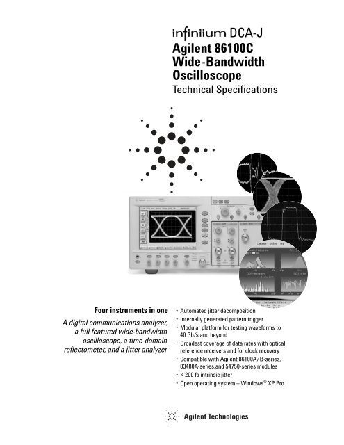
<strong>DCA</strong>-J<br />
<strong>Agilent</strong> <strong>86100C</strong><br />
<strong>Wide</strong>-<strong>Bandwidth</strong><br />
<strong>Oscilloscope</strong><br />
Technical Specifications<br />
Four instruments in one<br />
A digital communications analyzer,<br />
a full featured wide-bandwidth<br />
oscilloscope, a time-domain<br />
reflectometer, and a jitter analyzer<br />
• Automated jitter decomposition<br />
• Internally generated pattern trigger<br />
• Modular platform for testing waveforms to<br />
40 Gb/s and beyond<br />
• Broadest coverage of data rates with optical<br />
reference receivers and for clock recovery<br />
• Compatible with <strong>Agilent</strong> 86100A/B-series,<br />
83480A-series,and 54750-series modules<br />
• < 200 fs intrinsic jitter<br />
• Open operating system – Windows ® XP Pro
Table of Contents<br />
Overview<br />
Features 3<br />
Measurements 5<br />
Additional capabilities 6<br />
Specifications<br />
Mainframe & triggering<br />
(includes precision time base module) 10<br />
Computer system & storage 12<br />
Modules<br />
Overview 13<br />
Module selection table 14<br />
Specifications<br />
Multimode/single-mode 15<br />
Single-mode 19<br />
Dual electrical 20<br />
TDR 21<br />
Clock recovery 22<br />
Ordering Information 25<br />
2
Overview of infiniium <strong>DCA</strong>-J<br />
Features<br />
Four Instruments in One<br />
The <strong>86100C</strong> Infiniium <strong>DCA</strong>-J can be viewed as four<br />
high-powered instruments in one:<br />
• A general-purpose wide-bandwidth sampling<br />
oscilloscope; the new PatternLock triggering<br />
significantly enhances the usability as a general<br />
purpose scope<br />
• A digital communications analyzer; the new<br />
Eyeline Mode feature adds a powerful new tool to eye<br />
diagram analysis<br />
• A time domain reflectometer<br />
• A jitter analyzer<br />
Just select the desired instrument mode and start<br />
making measurements.<br />
Configurable to meet your needs<br />
The <strong>86100C</strong> supports a wide range of modules for testing<br />
both optical and electrical signals. Select modules to get<br />
the specific bandwidth, filtering, and sensitivity you need.<br />
PatternLock Triggering<br />
The Enhanced Trigger Option (Option 001) on the <strong>86100C</strong><br />
provides a fundamental capability never available<br />
before in an equivalent time sampling oscilloscope.<br />
This new triggering mechanism enables the <strong>DCA</strong>-J to<br />
generate a trigger at the repetition of the input data<br />
pattern – a pattern trigger. Historically, this capability<br />
required the pattern source to provide this type of<br />
trigger output to the scope. PatternLock automatically<br />
detects the pattern length, data rate and clock rate<br />
making the complex triggering mechanism transparent<br />
to the user.<br />
PatternLock enables the <strong>86100C</strong> to behave more like a<br />
real-time oscilloscope in terms of user experience.<br />
Investigation of specific bits within the data pattern is<br />
greatly simplified. Users that are familiar with real-time<br />
oscilloscopes, but perhaps less so with equivalent time<br />
sampling scopes will be able to ramp up quickly.<br />
PatternLock adds another new dimension to pattern<br />
triggering by enabling the mainframe software to take<br />
samples at specific locations in the data pattern with<br />
outstanding timebase accuracy. This capability is a<br />
building block for many of the new capabilities available<br />
in the <strong>86100C</strong> described later.<br />
Windows is a U.S. registered trademark of Microsoft Corporation.<br />
Jitter Analysis<br />
The “J” in <strong>DCA</strong>-J represents jitter analysis. The <strong>86100C</strong><br />
is a Digital Communications Analyzer with Jitter<br />
analysis capability. The <strong>86100C</strong> adds a fourth mode<br />
of operation – Jitter Mode. Extremely wide bandwidth,<br />
low intrinsic jitter, and advanced analysis algorithms<br />
yield the highest accuracy in jitter measurements.<br />
As data rates increase in both electrical and optical<br />
applications, jitter is an ever increasing measurement<br />
challenge. Decomposition of jitter into its constituent<br />
components is becoming more critical. It provides<br />
critical insight for jitter budgeting and performance<br />
optimization in device and system designs. Many<br />
emerging standards require jitter decomposition for<br />
compliance. Traditionally, techniques for separation of<br />
jitter have been complex and often difficult to configure,<br />
and availability of instruments for separation of jitter<br />
becomes very limited as data rates increase.<br />
The <strong>DCA</strong>-J provides simple, one button setup and<br />
execution of advanced waveform analysis. Jitter Mode<br />
decomposes jitter into its constituent components and<br />
presents jitter data in various insightful displays. Jitter<br />
Mode operates at all data rates the <strong>86100C</strong> supports,<br />
removing the traditional data rate limitations from<br />
complex jitter analysis. The <strong>86100C</strong> brings several<br />
key attributes to jitter analysis:<br />
• Very low intrinsic jitter (both random and<br />
deterministic) translates to a very low jitter noise<br />
floor which provides unmatched jitter measurement<br />
sensitivity.<br />
• <strong>Wide</strong> bandwidth measurement channels deliver very<br />
low intrinsic data dependent jitter and allow analysis<br />
of jitter on all data rates to 40 Gb/s and beyond.<br />
• PatternLock triggering technology provides sampling<br />
efficiency that makes jitter measurements very fast.<br />
Jitter analysis functionality is segmented into two<br />
software package options. Option 200 is the enhanced<br />
jitter analysis software, and Option 201 is the advanced<br />
waveform analysis software. Option 200 includes:<br />
• Decomposition of jitter into Total Jitter (TJ), Random<br />
Jitter (RJ), Deterministic Jitter (DJ), Periodic Jitter<br />
(PJ), Data Dependent Jitter (DDJ), Duty Cycle<br />
Distortion (DCD), and Jitter induced by Intersymbol<br />
Interference (ISI).<br />
• Various graphical and tabular displays of jitter data<br />
• Export of jitter data to convenient delimited text format<br />
• Save / recall of jitter database<br />
• Jitter frequency spectrum<br />
• Isolation and analysis of Sub-Rate Jitter (SRJ), that is,<br />
periodic jitter that is at an integer sub-rate of the bitrate.<br />
• Bathtub curve display<br />
• Adjustable total jitter probability<br />
3
4<br />
Equalization Capabilities<br />
As bit rates increase, channel effects cause significant<br />
eye closure. Many new devices and systems are<br />
employing equalization and pre/de-emphasis to<br />
compensate for channel effects. Option 201 Advanced<br />
Waveform Analysis will provide key tools to enable<br />
design and test of devices and systems that must deal<br />
with difficult channel effects:<br />
• Capture of long single valued waveforms. PatternLock<br />
triggering and the waveform append capability of<br />
Option 201 enable very accurate pulse train data sets<br />
up to 256 megasamples long.<br />
• Equalization. The <strong>DCA</strong>-J can take a long single<br />
valued waveform and route it through a linear<br />
equalizer algorithm (default or user defined) and<br />
display the resultant equalized waveform in real time.<br />
The user can simultaneously view the input (distorted)<br />
and output (equalized) waveforms.<br />
• Interface to MATLAB® analysis capability.<br />
Digital communications analysis<br />
Accurate eye-diagram analysis is essential for<br />
characterizing the quality of transmitters used<br />
from 100 Mb/s to 40 Gb/s. The <strong>86100C</strong> is designed<br />
specifically for the complex task of analyzing digital<br />
communications waveforms. Compliance mask and<br />
parametric testing no longer require a complicated<br />
sequence of setups and configurations. If you can press<br />
a button, you can perform a complete compliance test.<br />
The important measurements you need are right at your<br />
fingertips, including:<br />
• industry standard mask testing with built-in<br />
margin analysis<br />
• extinction ratio measurements with accuracy and<br />
repeatability<br />
• eye measurements: crossing %, eye height and width,<br />
‘1’ and ‘0’ levels, jitter, rise or fall times and more<br />
The key to accurate measurements of lightwave<br />
communications waveforms is the optical receiver.<br />
The <strong>86100C</strong> has a broad range of precision receivers<br />
integrated within the instrument.<br />
• Built-in photodiodes, with flat frequency responses,<br />
yield the highest waveform fidelity. This provides high<br />
accuracy for extinction ratio measurements.<br />
• Standards-based transmitter compliance measurements<br />
require filtered responses. The <strong>86100C</strong> has a broad<br />
range of filter combinations. Filters can be automatically<br />
and repeatably switched in or out of the measurement<br />
channel remotely over GPIB or with a front panel<br />
button. The frequency response of the entire<br />
measurement path is calibrated, and will maintain<br />
its performance over long-term usage.<br />
• The integrated optical receiver provides a calibrated<br />
optical channel. With the accurate optical receiver<br />
built into the module, optical signals are accurately<br />
measured and displayed in optical power units.<br />
Switches or couplers are not required for an average<br />
power measurement. Signal routing is simplified and<br />
signal strength is maintained.<br />
Eye diagram mask testing<br />
The <strong>86100C</strong> provides efficient, high-throughput<br />
waveform compliance testing with a suite of standards<br />
based eye-diagram masks. The test process has been<br />
streamlined into a minimum number of keystrokes for<br />
testing at industry standard data rates.<br />
Standard formats<br />
Rate<br />
(Mb/s)<br />
1X Gigabit Ethernet 1250<br />
2X Gigabit Ethernet 2500<br />
10 Gigabit Ethernet 9953.28<br />
10 Gigabit Ethernet 10312.5<br />
10 Gigabit Ethernet FEC 11095.7<br />
10 Gigabit Ethernet LX4 3125<br />
Fibre Channel 1062.5<br />
2X Fibre Channel 2125<br />
4X Fibre Channel 4250<br />
8x Fibre Channel 8500<br />
10X Fibre Channel 10518.75<br />
10X Fibre Channel FEC 11317<br />
Infiniband 2500<br />
STM0/OC1 51.84<br />
STM1/OC3 155.52<br />
STM4/OC12 622.08<br />
STM16/OC48 2488.3<br />
STM16/OC48 FEC 2666<br />
STM64/OC192 9953.28<br />
STM64/OC192 FEC 10664.2<br />
STM64/OC192 FEC 10709<br />
STM64/OC192 Super FEC 12500<br />
STM256/OC768 39813<br />
STS1 EYE 51.84<br />
STS3 EYE 155.52<br />
Other eye-diagram masks are easily created through<br />
scaling those listed at left. In addition, mask editing<br />
allows for new masks either by editing existing masks,<br />
or creating new masks from scratch. A new mask can<br />
also be created or modified on an external PC using<br />
a text editor such as Notepad, then can be transferred<br />
to the instrument’s hard drive using LAN or Flash drive.<br />
Perform these mask conformance tests with convenient<br />
user-definable measurement conditions, such as mask<br />
margins for guardband testing, number of waveforms<br />
tested, and stop/limit actions.
Eyeline Mode<br />
Eyeline Mode is a new feature only available in the<br />
<strong>86100C</strong> that provides insight into the effects of specific<br />
bit transitions within a data pattern. The unique view<br />
assists diagnosis of device or system failures do to<br />
specific transitions or sets of transitions within a<br />
pattern. When combined with mask limit tests, Eyeline<br />
Mode can quickly isolate the specific bit that caused a<br />
mask violation.<br />
Traditional triggering methods on an equivalent time<br />
sampling scope are quite effective at generating eye<br />
diagrams. However, these eye diagrams are made up of<br />
samples whose timing relationship to the data pattern is<br />
effectively random, so a given eye will be made up of<br />
samples from many different bits in the pattern taken<br />
with no specific timing order. The result is that<br />
amplitude versus time trajectories of specific bits in<br />
the pattern are not visible. Also, averaging of the eye<br />
diagram is not valid, as the randomly related samples<br />
will effectively average to zero.<br />
Eyeline Mode uses PatternLock triggering to build up an<br />
eye diagram from samples taken sequentially through<br />
the data pattern. This maintains a specific timing<br />
relationship between samples and allows Eyeline Mode<br />
to draw the eye based on specific bit trajectories.<br />
Effects of specific bit transitions can be investigated,<br />
and averaging can be used with the eye diagram.<br />
Measurement speed<br />
Measurement speed has been increased with both fast<br />
hardware and a user-friendly instrument. In the lab,<br />
don’t waste time trying to figure out how to make a<br />
measurement. With the simple-to-use <strong>86100C</strong>, you don’t<br />
have to relearn how to make a measurement each time<br />
you use it.<br />
Manufacturers are continually forced to reduce the cost<br />
per test. Solution: Fast PC-based processors, resulting in<br />
high measurement throughput and reduced test time.<br />
Measurements<br />
The following measurements are available from the tool<br />
bar, as well as the pull down menus. The available<br />
measurements depend on the <strong>DCA</strong>-J operating mode.<br />
<strong>Oscilloscope</strong> mode<br />
Time<br />
Rise Time, Fall Time, Jitter RMS, Jitter p-p, Period,<br />
Frequency, + Pulse Width, - Pulse Width, Duty Cycle,<br />
Delta Time, [T max , T min , T edge —remote commands only]<br />
Amplitude<br />
Overshoot, Average Power, V amptd, V p-p, V rms,<br />
V top, V base, V max, V min, V avg<br />
Eye/mask mode<br />
NRZ eye measurements<br />
Extinction Ratio, Jitter RMS, Jitter p-p, Average Power,<br />
Crossing Percentage, Rise Time, Fall Time, One Level,<br />
Zero Level, Eye Height, Eye Width, Signal to Noise<br />
(Q-Factor), Duty Cycle Distortion, Bit Rate,<br />
Eye Amplitude<br />
RZ Eye Measurements<br />
Extinction Ratio, Jitter RMS, Jitter p-p, Average Power,<br />
Rise Time, Fall Time, One Level, Zero Level, Eye Height,<br />
Eye Amplitude, Opening Factor, Eye Width, Pulse<br />
Width, Signal to Noise (Q-Factor), Duty Cycle, Bit Rate,<br />
Contrast Ratio<br />
Mask Test<br />
Open Mask, Start Mask Test, Exit Mask Test, Filter,<br />
Mask Test Margins, Mask Test Scaling, Create NRZ Mask<br />
Jitter Mode<br />
Jitter Mode requires Option 001 Enhanced Trigger hardware.<br />
There are two analysis software packages for the <strong>DCA</strong>-J.<br />
Option 200 is the enhanced jitter analysis software, and<br />
Option 201 is the advanced waveform analysis software.<br />
Measurements (Option 200 Jitter Analysis)<br />
Total Jitter (TJ), Random Jitter (RJ), Deterministic<br />
Jitter (DJ), Periodic Jitter (PJ), Data Dependent<br />
Jitter (DDJ), Duty Cycle Distortion (DCD), Intersymbol<br />
Interference (ISI), Sub-Rate Jitter (SRJ)<br />
Data Displays (Option 200 Jitter Analysis)<br />
TJ histogram, RJ/PJ histogram, DDJ histogram,<br />
Composite histogram, DDJ versus Bit position,<br />
Bathtub curve, SRJ analysis<br />
Measurements (Option 201 Advanced<br />
Waveform Analysis)<br />
Pattern waveform<br />
Data Displays (Option 201 Advanced<br />
Waveform Analysis)<br />
Equalized waveform<br />
TDR/TDT Mode (requires TDR module)<br />
Quick TDR, TDR/TDT Setup, Normalize, Response,<br />
Rise Time, Fall Time, ∆ Time, Minimum Impedance,<br />
Maximum Impedance, Average Impedance,<br />
Single-ended and Mixed-mode S-parameters.<br />
5
Additional Capabilities<br />
Standard Functions<br />
Standard functions are available through pull down<br />
menus and soft keys, and some functions are also<br />
accessible through the front panel knobs.<br />
Markers<br />
Two vertical and two horizontal (user selectable)<br />
TDR Markers<br />
Horizontal — seconds or meter<br />
Vertical — volts, ohms or Percent Reflection<br />
Propagation — Dielectric Constant or Velocity<br />
Limit tests<br />
Acquisition limits<br />
Limit Test Run Until Conditions — Off, # of Waveforms,<br />
# of Samples<br />
Report Action on Completion — Save waveform to<br />
memory or disk, Save screen image to disk<br />
Measurement limit test<br />
Specify Number of Failures to Stop Limit Test<br />
When to Fail Selected Measurement — Inside Limits,<br />
Outside Limits, Always Fail, Never Fail<br />
Report Action on Failure - Save waveform to memory<br />
or disk, Save screen image to disk, Save summary<br />
to disk<br />
Mask limit test<br />
Specify Number of Failed Mask Test Samples<br />
Report Action on Failure — Save waveform to memory<br />
or disk, Save screen image to disk, Save summary<br />
to disk<br />
Configure measurements<br />
Thresholds<br />
10%, 50%, 90% or 20%, 50%, 80% or Custom<br />
Eye Boundaries<br />
Define boundaries for eye measurments<br />
Define boundaries for alignment<br />
Format Units for<br />
Duty Cycle Distortion — Time or Percentage<br />
Extinction/Contrast Ratio — Ratio, Decibel<br />
or Percentage<br />
Eye Height — Amplitude or Decibel (dB)<br />
Eye Width — Time or Ratio<br />
Average Power — Watts or Decibels (dB)<br />
Top Base Definition<br />
Automatic or Custom<br />
∆ Time Definition<br />
First Edge Number, Edge Direction, Threshold<br />
Second Edge Number, Edge Direction, Threshold<br />
Jitter Mode<br />
Units (time or unit interval)<br />
Signal type (data or clock)<br />
Measure based on edges (all, rising only, falling only)<br />
Graph layout ( single, split, quad)<br />
Quick Measure Configuration<br />
4 User Selectable Measurements for Each Mode<br />
Default Settings<br />
(Eye/Mask Mode)<br />
Extinction Ratio, Jitter RMS, Average Power,<br />
Crossing Percentage<br />
Default Settings<br />
(<strong>Oscilloscope</strong> Mode)<br />
Rise Time, Fall Time, Period,<br />
V amptd<br />
Histograms<br />
Configure<br />
Histogram scale (1 to 8 divisions)<br />
Histogram axis (vertical or horizontal)<br />
Histogram window (adjustable Window via<br />
marker knobs)<br />
Math measurements<br />
4 User definable functions Operator — magnify,<br />
invert, subtract, versus, min, max<br />
Source — channel, function, memory, constant,<br />
response (TDR)<br />
Calibrate<br />
All calibrations<br />
Module (amplitude)<br />
Horizontal (time base)<br />
Extinction ratio<br />
Probe<br />
Optical channel<br />
Front panel calibration output level<br />
User selectable –2V to 2V<br />
Utilities<br />
Set time and date<br />
Remote interface<br />
Set GPIB interface<br />
Touch screen configuration/calibration<br />
Calibration<br />
Disable/enable touch screen<br />
Upgrade software<br />
Upgrade mainframe<br />
Upgrade module<br />
6
Built-in information system<br />
The <strong>86100C</strong> has a context-sensitive on-line<br />
manual providing immediate answers to your<br />
questions about using the instrument. Links on<br />
the measurement screen take you directly to the<br />
information you need including algorithms for all of the<br />
measurements. The on-line manual includes technical<br />
specifications of the mainframe and plug-in modules. It<br />
also provides useful information such as the mainframe<br />
serial number, module serial numbers, firmware revision<br />
and date, and hard disk free space. There is no need for a<br />
large paper manual consuming your shelf space.<br />
File sharing and storage<br />
Use the internal 40 GB hard drive to store instrument<br />
setups, waveforms, or screen images. A 64MB USB<br />
memory stick is included with the mainframe. Combined<br />
with the USB port on the front panel this provides for<br />
quick and easy file transfer. Images can be stored in<br />
formats easily imported into various programs for<br />
documentation and further analysis. LAN interface is<br />
also available for network file management and printing.<br />
An external USB CD-RW drive is included with the<br />
mainframe. This enables easy installation of software<br />
applications as well as storage of large amounts of data.<br />
File security<br />
For users requiring security of their data, <strong>86100C</strong><br />
Option 090 offers a removable hard drive. This also<br />
enables removal of the mainframe from secure<br />
environments for calibration and repair.<br />
Powerful display modes<br />
Use gray scale and color graded trace displays to gain<br />
insight into device behavior. Waveform densities are<br />
mapped to color or easy-to-interpret gray shades.<br />
These are infinite persistence modes where shading<br />
differentiates the number of times data in any individual<br />
screen pixel has been acquired.<br />
Direct triggering through clock recovery<br />
Typically an external timing reference is used to<br />
synchronize the oscilloscope to the test signal. In cases<br />
where a trigger signal is not available, clock recovery<br />
modules are available to derive a timing reference<br />
directly from the waveform to be measured. The <strong>Agilent</strong><br />
8349XA series of clock recovery modules are available<br />
for electrical, multimode optical, and single-mode optical<br />
input signals. All 8349XA modules have excellent jitter<br />
performance to ensure accurate measurements. Each<br />
clock recovery module is designed to synchronize to a<br />
variety of common transmission rates. The 83496A can<br />
derive triggering from optical and electrical signals at<br />
any rate from 50 Mb/s to 13.5 Gb/s.<br />
Clock recovery loop bandwidth<br />
The <strong>Agilent</strong> clock recovery modules have adjustable loop<br />
bandwidth settings. Loop bandwidth is very important<br />
in determining the accuracy of your waveform when<br />
measuring jitter, as well as testing for compliance. When<br />
using recovered clocks for triggering, the amount of<br />
jitter observed will depend on the loop bandwidth. As<br />
the loop bandwidth increases, more jitter is “tracked out”<br />
by the clock recovery resulting in less observed jitter.<br />
• Narrow loop bandwidth provides a “jitter free” system<br />
clock to observe all the jitter<br />
• <strong>Wide</strong> loop bandwidth in some applications is specified<br />
in the standards for compliance testing. <strong>Wide</strong> loop<br />
bandwidth settings mimic the performance of<br />
communications system receivers<br />
The 83496A has a continuously adjustable loop bandwidth<br />
from as low as 30 kHz to as high as 10 MHz, and can be<br />
configured as a golden PLL for standards compliance<br />
testing.<br />
7
S-parameters and time domain<br />
reflectometery/time domain transmission<br />
(TDR/TDT)<br />
High-speed design starts with the physical structure.<br />
The transmission and reflection properties of electrical<br />
channels and components must be characterized to<br />
ensure sufficient signal integrity, so reflections and<br />
signal distortions must be kept at a minimum. Use TDR<br />
and TDT to optimize microstrip lines, backplanes, PC<br />
board traces, SMA edge launchers and coaxial cables.<br />
Analyze return loss, attenuation, crosstalk, and other<br />
S-parameters with one button push using the <strong>86100C</strong><br />
Option 202 Enhanced Impedance and S-parameter<br />
software, either in single-ended or mixed-mode signals.<br />
Calibration techniques, unique to the <strong>86100C</strong>, provide<br />
highest precision by removing cabling and fixturing<br />
effects from the measurement results. Translation of TDR<br />
data to complete single-ended, differential, and mixed<br />
mode S-parameters are available through Option 202 and<br />
the N1930A Physical Layer Test System software. Higher<br />
two-event resolution and ultra high-speed impedance<br />
measurements are facilitated through TDR pulse<br />
enhancers from Picosecond Pulse Labs 1 .<br />
N1024 TDR calibration kit<br />
The N1024A TDR calibration kit contains precision<br />
standard devices based on SOLT (Short-Open-Load-<br />
Through) technology to calibrate the measurement path.<br />
Waveform autoscaling<br />
Autoscaling provides quick horizontal and vertical scaling<br />
of both pulse and eye-diagram (RZ and NRZ) waveforms.<br />
Gated triggering<br />
Trigger gating port allows easy external control of data<br />
acquisition for circulating loop or burst-data<br />
experiments. Use TTL-compatible signals to control<br />
when the instrument does and does not acquire data.<br />
Easier calibrations<br />
Calibrating your instrument has been simplified by<br />
placing all the performance level indicators and<br />
calibration procedures in a single high-level location.<br />
This provides greater confidence in the measurements<br />
made and saves time in maintaining equipment.<br />
Stimulus response testing using the<br />
<strong>Agilent</strong> N490X BERTs<br />
Error performance analysis represents an essential part<br />
of digital transmission test. The <strong>Agilent</strong> <strong>86100C</strong> and<br />
N490X BERT have similar user interfaces and together<br />
create a powerful test solution. If stimulus only is<br />
needed, the 81141A and 81142A pattern generators<br />
work seamlessly with the <strong>86100C</strong>.<br />
Transitioning from the <strong>Agilent</strong> 83480A and<br />
86100A/B to the <strong>86100C</strong><br />
While the <strong>86100C</strong> has powerful new functionality that<br />
its predecessors don’t have, it has been designed to<br />
maintain compatibility with the <strong>Agilent</strong> 86100A, 86100B<br />
and <strong>Agilent</strong> 83480A digital communications analyzers<br />
and <strong>Agilent</strong> 54750A wide-bandwidth oscilloscope. All<br />
modules used in the <strong>Agilent</strong> 86100A/B, 83480A and<br />
54750A can also be used in the <strong>86100C</strong>. The remote<br />
programming command set for the <strong>86100C</strong> has been<br />
designed so that code written for the 86100A or 86100B<br />
will work directly. Some code modifications are required<br />
when transitioning from the 83480A and 54750A, but<br />
the command set is designed to minimize the level of<br />
effort required.<br />
IVI-COM capability<br />
Interchangeable Virtual Instruments (IVI) is a group of<br />
new instrument device software specifications created<br />
by the IVI Foundation to simplify interchangeability,<br />
increase application performance, and reduce the cost<br />
of test program development and maintenance through<br />
design code reuse. The <strong>86100C</strong> IVI-COM drivers are<br />
available for download from the <strong>Agilent</strong> website.<br />
1 Picosecond Pulse Labs (www.picosecond.com)<br />
8
Lowest intrinsic jitter<br />
The patented 86107A precision timebase reference<br />
module represents one of the most significant<br />
improvements in wide-bandwidth sampling oscilloscopes<br />
in over a decade. Jitter performance has been reduced<br />
by almost an order of magnitude to < 200 fs RMS.<br />
<strong>Oscilloscope</strong> jitter is virtually eliminated! The reduced<br />
jitter of the 86107A precision timebase module allows<br />
you to measure the true jitter of your signal. When using<br />
the 86107A, the minimum timebase resolution for<br />
oscilloscope and eye/mask displays is 500 fs/division,<br />
rather than 2 ps/div with the standard timebase.<br />
The standard timebase of the <strong>86100C</strong> has very low<br />
intrinsic jitter compared to other advanced waveform<br />
analysis solutions. However, for users who need the most<br />
accurate sensitivity for their jitter measurements, the<br />
86107A provides the ultimate timebase performance.<br />
Using the 86107A with Jitter Mode requires the<br />
Option 200 Enhanced Jitter software package. Jitter<br />
measurements with the 86107A are targeted at users<br />
who are trying to accurately measure very low levels of<br />
jitter and need to minimize the jitter contribution of the<br />
scope.<br />
The 86107A requires an electrical reference clock that is<br />
synchronous with the signal under test. For specific<br />
requirements of the clock signal, see the 86107A<br />
specifications on page 11.<br />
Accurate views of your 40 Gb/s<br />
waveforms<br />
When developing 40 Gb/s devices, even a small amount of<br />
inherent scope jitter can become significant since 40 Gb/s<br />
waveforms only have a bit period of 25 ps. Scope jitter<br />
of 1ps RMS can result in 6 to 9 ps of peak-to-peak jitter,<br />
causing eye closure even if your signal is jitter-free. The<br />
<strong>Agilent</strong> 86107A reduces the intrinsic jitter of 86100<br />
family mainframes to the levels necessary to make<br />
quality waveform measurements on 40 Gb/s signals.<br />
Meeting your growing need for more bandwidth<br />
Today’s communication signals have significant<br />
frequency content well beyond an oscilloscope’s 3-dB<br />
bandwidth. A high-bandwidth scope does not alone<br />
guarantee an accurate representation of your waveform.<br />
Careful design of the scope’s frequency response (both<br />
amplitude and phase) minimizes distortion such as<br />
overshoot and ringing.<br />
The <strong>Agilent</strong> 86116A and 86116B are plug-in modules<br />
that include an integrated optical receiver designed<br />
to provide the optimum in bandwidth, sensitivity, and<br />
waveform fidelity. The 86116B extends the bandwidth<br />
of the <strong>86100C</strong> infiniium <strong>DCA</strong>-J to 80 GHz electrical,<br />
65 GHz optical in the 1550 nm wavelength band. The<br />
86116A covers the 1300 nm and 1550 nm wavelength<br />
bands with 63 GHz of electrical bandwidth and 53 GHz<br />
of optical bandwidth. The 86117A and 86118A modules<br />
provide electrical bandwidth to 50 GHz and 70 gHz<br />
respectively. You can build the premier solution for<br />
40 Gb/s waveform analysis around the 86100 mainframe<br />
that you already own.<br />
Performing return-to-zero<br />
(RZ) waveform measurements<br />
An extensive set of automatic RZ measurements are<br />
built-in for the complete characterization of return-to-zero<br />
(RZ) signals at the push of a button.<br />
The same 40 GHz sinewave<br />
captured using current <strong>DCA</strong> (top)<br />
and now with 86107A precision<br />
timebase module (bottom).<br />
9
Specifications<br />
Specifications describe warranted performance over the temperature range of +10 °C to +40 °C (unless otherwise noted). The specifications are<br />
applicable for the temperature after the instrument is turned on for one (1) hour, and while self-calibration is valid. Many performance parameters are<br />
enhanced through frequent, simple user calibrations. Characteristics provide useful, non-warranted information about the functions and<br />
performance of the instrument. Characteristics are printed in italic typeface.<br />
Factory Calibration Cycle -For optimum performance, the instrument should have a complete verification of specifications once every twelve (12) months.<br />
General specifications<br />
This instrument meets <strong>Agilent</strong> Technologies’ environmental specifications (section 750) for class B-1 products with exception as described for temperature and<br />
condensation. Contact your local field engineer for complete details. Product specifications and descriptions in this document subject to change without notice.<br />
Temperature<br />
Operating<br />
Non-operating<br />
Humidity<br />
Operating<br />
Non-operating<br />
Altitude<br />
Operating<br />
Non-operating<br />
Vibration<br />
Operating<br />
Non-operating<br />
Power requirements<br />
Voltage<br />
Power (including modules)<br />
Weight<br />
Mainframe without modules<br />
Typical module<br />
Mainframe dimensions (excluding handle)<br />
Without front connectors and rear feet<br />
With front connectors and rear feet<br />
10 °C to +40 °C (50 °F to +104 °F)<br />
–40 °C to +65 °C (–40 °F to +158 °F)<br />
Up to 90% humidity (non-condensing) at +40 °C (+104 °F)<br />
Up to 95% relative humidity at +65 °C (+149 °F)<br />
Up to 4,600 meters (15,000 ft)<br />
Up to 15,300 meters (50,000 ft)<br />
Random vibration 5 to 500 Hz, 10 minutes per axis, 0.21 g (rms)<br />
Random vibration 5 to 500 Hz, 10 minutes per axis, 0.3 g (rms); Resonant search, 5 to 500 Hz<br />
swept sine, 1 octave/min sweep rate, 0.5 g, 5 minute resonant dwell at 4 resonances/axis<br />
90 to 132 or 198 to 264 Vac, 48 to 66 Hz<br />
604 VA; 391 W<br />
15.5 kg (34 lb)<br />
1.2 kg (2.6 lb)<br />
215.1 mm H x 425.5 mm W x 566 mm D (8.47 in x 16.75 in x 22.2 in)<br />
215.1 mm H x 425.5 mm W x 629 mm D (8.47 in x 16.75 in x 24.8 in)<br />
10<br />
Mainframe specifications<br />
HORIZONTAL SYSTEM (time base)<br />
PATTERN LOCK<br />
Scale factor (full scale is ten divisions)<br />
Minimum<br />
2 ps/div (with 86107A: 500 fs/div)<br />
Maximum 1 s/div 250 ns/div<br />
Delay 1<br />
Minimum 24 ns 40.1 ns<br />
Maximum 1000 screen diameters or 10 s, 1000 screen diameters or 25.401 µs,<br />
whichever is smaller<br />
whichever is smaller<br />
Time interval accuracy 2 1 ps + 1.0% of ∆ time reading 3<br />
8 ps + 0.1% of ∆ time reading<br />
Time interval accuracy – jitter mode operation 4 1 ps<br />
Time interval accuracy – with 86107A<br />
< 200 fs<br />
precision timebase<br />
Time interval resolution<br />
≤ (screen diameter)/(record length) or 62.5 fs,<br />
whichever is larger<br />
Display units<br />
Bits or time (TDR mode–meters)<br />
VERTICAL SYSTEM (channels)<br />
Number of channels<br />
4 (simultaneous acquisition)<br />
Vertical resolution<br />
14 bit A/D converter (up to 15 bits with averaging)<br />
Full resolution channel scales<br />
Adjusts in a 1-2-5-10 sequence for coarse adjustment or fine adjustment resolution<br />
from the front panel knob<br />
Adjustments<br />
Scale, offset, activate filter, sampler bandwidth, attenuation factor, transducer conversion factors<br />
Record length 16 to 4096 samples – increments of 1<br />
1 Time offset relative to the front panel trigger input on the instrument mainframe.<br />
2 Dual marker measurement performed at a temperature within ±5 °C of horizontal calibration temperature.<br />
3 Delay settings: ∆ time is in the range (26 + N*4 ns) ±1.9 ns, where N = 0, 1, 2, ... 17.<br />
4 Characteristic performance. Test configuration: PRBS of length 2 7 – 1 bits, Data and Clock 10 Gb/s.
Mainframe specifications (continued)<br />
Standard (direct trigger)<br />
Option 001 (enhanced trigger)<br />
Trigger Modes<br />
Internal trigger 1<br />
Free run<br />
External direct trigger 2<br />
Limited bandwidth 3<br />
DC to 100 MHz<br />
Full bandwidth<br />
DC to 3.2 GHz<br />
External Divided Trigger N/A 3 GHz to 13 GHz (3 GHz to 15 GHz)<br />
PatternLock N/A 50 MHz to 13 GHz (50 MHz to 15 GHz)<br />
Jitter<br />
Characteristic < 1.0 ps RMS + 5*10E-5 of delay setting 4 1.2 ps RMS for time delays less than 100 ns 6<br />
Maximum 1.5 ps RMS + 5*10E-5 of delay setting 4 1.7 ps RMS for time delays less than 100 ns 6<br />
Trigger sensitivity 200 m Vpp (sinusoidal input or 200 m Vpp sinusoidal input: 50 MHz to 8 GHz<br />
200 ps minimum pulse width) 400 m Vpp sinusoidal input: 8 GHz to 13 GHz<br />
600 m Vpp sinusoidal input: 13 GHz to 15 GHz<br />
Trigger configuration<br />
Trigger level adjustment –1 V to + 1 V AC coupled<br />
Edge select Positive or negative N/A<br />
Hysteresis 5 Normal or high sensitivity N/A<br />
Trigger gating<br />
Gating input levels<br />
Disable: 0 to 0.6 V<br />
(TTL compatible)<br />
Enable: 3.5 to 5 V<br />
Pulse width > 500 ns, period > 1 µs<br />
Gating delay Disable: 27 ns + trigger period +<br />
Max time displayed<br />
Enable: 100 ns<br />
Trigger impedance<br />
Nominal impedance<br />
50 Ω<br />
Reflection<br />
10% for 100 ps rise time<br />
Connector type<br />
3.5 mm (male)<br />
Maximum trigger signal<br />
2 V peak-to-peak<br />
1 The freerun trigger mode internally generates an asynchronous trigger that allows viewing the sampled signal amplitude without an external trigger signal but provides no timing information. Freerun is useful in<br />
troubleshooting external trigger problems.<br />
2 The sampled input signal timing is recreated by using an externally supplied trigger signal that is synchronous with the sampled signal input.<br />
3 The DC to 100 MHz mode is used to minimize the effect of high frequency signals or noise on a low frequency trigger signal.<br />
4 Measured at 2.5 GHz with the triggering level adjusted for optimum trigger.<br />
5 High Sensitivity Hysteresis Mode improves the high frequency trigger sensitivity but is not recommended when using noisy, low frequency signals that may result in false triggers without normal hysteresis enabled.<br />
6 Slew rate ≥ 2V/ns<br />
Precision time base 86107A 1 86107A Option 010 86107A Option 020 86107A Option 040<br />
Trigger bandwidth 2.4 to 15.0 GHz 2.4 to 25.0 GHz 2.4 to 48.0 GHz<br />
Typical jitter (RMS) 2.4 to 4.0 GHz trigger: < 280 fs 2.4 to 4.0 GHz < 280 fs 2.4 to 4.0 GHz < 280 fs<br />
4.0 to 15.0 GHz trigger: < 200 fs 4.0 to 25.0 GHz < 200 fs 4.0 to 48.0 GHz < 200 fs<br />
Time base linearity error<br />
< 200 fs<br />
Input signal type Synchronous clock 2<br />
Input signal level<br />
0.5 to 1.0 Vpp<br />
0.2 to 1.5 Vpp (Typical functional performance)<br />
DC offset range ±200 mV 3<br />
Required trigger signal-to-noise ratio ≥ 200 : 1<br />
Trigger gating<br />
Disable: 0 to 0.6 V<br />
Gating input levels (TTL compatible) Enable: 3.5 to 5 V<br />
Pulse width > 500 ns, period > 1 µs<br />
Trigger impedance (nominal)<br />
50 Ω<br />
Connector type 3.5 mm (male) 3.5 mm (male)<br />
2.4 mm (male)<br />
1 Requires 86100 software revision 4.1 or above.<br />
2 Filtering provided for Option 010 bands 2.4 to 4.0 GHz and 9.0 to 12.6 GHz, for Option 020 9.0 to 12.6 GHz and 18 to 25.0 GHz, for Option 40 9.0 to 12.6 GHz, 18.0 to 25.0 GHz, and 39.0 to<br />
48.0 GHz. Within the filtered bands, a synchronous clock signal should be provided (clock, sinusoid, BERT trigger, etc.). Outside these bands, filtering is required to minimize harmonics and sub<br />
harmonics and provide a sinusoid to the 86107 input.<br />
3 For the 86107A with Option 020, the <strong>Agilent</strong> 11742A (DC Block) is recommended if the DC offset magnitude is greater than 200 mV.<br />
11
Computer system and storage<br />
CPU<br />
Mass storage<br />
1 GHz microprocessor<br />
40 GByte internal hard drive<br />
External USB CD-RW drive<br />
64 MB USB pen memory<br />
Operating System<br />
Microsoft Windows ® XP Pro<br />
DISPLAY 1<br />
Display area<br />
170.9 mm x 128.2 mm (8.4 inch diagonal color active matrix LCD module incorporating amorphous<br />
silicon TFTs)<br />
Active display area<br />
171mm x 128 mm (21,888 square mm) 6.73 in x 5.04 in (33.92 square inches)<br />
Waveform viewing area<br />
103 mm x 159 mm (4.06 in x 6.25 in)<br />
Entire display resolution<br />
640 pixels horizontally x 480 pixels vertically<br />
Graticule display resolution<br />
451 pixels horizontally x 256 pixels vertically<br />
Waveform colors<br />
Select from 100 hues, 0 to 100% saturation and 0 to 100% luminosity<br />
Persistence modes<br />
Gray scale, color grade, variable, infinite<br />
Waveform overlap<br />
When two waveforms overlap, a third color distinguishes the overlap area<br />
Connect-the-dots<br />
On/Off selectable<br />
Persistence<br />
Minimum, variable (100 ms to 40 s), infinite<br />
Graticule<br />
On/Off<br />
Grid intensity 0 to 100%<br />
Backlight saver<br />
2 to 8 hrs, enable option<br />
Dialog boxes<br />
Opaque or transparent<br />
FRONT PANEL<br />
INPUTS AND OUTPUTS<br />
Cal output<br />
BNC (female) and test clip, banana plug<br />
Trigger input<br />
APC 3.5 mm, 50 Ω, 2 Vpp base max<br />
USB 2<br />
REAR PANEL<br />
INPUTS AND OUTPUTS<br />
Gated trigger input<br />
TTL compatible<br />
Video output VGA, full color, 15 pin D-sub (female) 10<br />
GPIB Fully programmable, complies with IEEE 488.2<br />
RS-232<br />
Serial printer, 9 pin D-sub (male)<br />
Centronics<br />
Parallel printer port, 25 pin D-sub (female)<br />
LAN<br />
USB 2 (2)<br />
1 Supports external display. Supports multiple display configurations via Windows® XP Pro display utility.<br />
2 USB Keyboard and mouse included with mainframe. Keyboard has intergrated, 2-port USB hub.<br />
MS-DOS and Windows XP Pro are U.S. registered trademarks of Microsoft Corporation.<br />
12
Module overview<br />
Optical/electrical modules<br />
750-1650 nm<br />
The 86105C has the widest coverage of data rates with<br />
optical bandwidth of 9 GHz and electrical bandwidth of<br />
20 GHz. The outstanding sensitivity up to –21 dBm<br />
makes the 86105C ideal for a wide range of design and<br />
manufacturing applications. Available filters cover all<br />
common data rates from 155 Mb/s through 11.3 Gb/s.<br />
750-860 nm<br />
The 86102U module supports waveform compliance<br />
testing of short wavelength signals with up to 15 GHz of<br />
optical bandwidth and 20 GHz of electrical bandwidth.<br />
1000–1600 nm<br />
< 20 GHz Optical and Electrical Channels:<br />
The 86105B module is optimized for testing long<br />
wavelength signals with up to 15 GHz of optical<br />
bandwidth. Each module also has an electrical channel<br />
with 20 GHz of bandwidth.<br />
The 86105B provides the high pulse fidelity and<br />
sensitivity, and flexible data rates. It is the recommended<br />
module for 10 Gb/s compliance applications.<br />
20 to 40 GHz Optical and Electrical Channels:<br />
The 86106B has 28 GHz of optical bandwidth with<br />
multiple 10Gb/s compliance filters, and has an electrical<br />
channel with 40 GHz of bandwidth.<br />
40 GHz and Greater Optical and Electrical Channels:<br />
The 86116A is optimized for testing 40 Gb/s signals. The<br />
86116A has more than 50 GHz of optical bandwidth and<br />
60 GHz of electrical bandwidth. The 86116B is the widest<br />
bandwidth optical module with more than 65 GHz optical<br />
(1550nm band only) and 80 GHz electrical bandwidth.<br />
Dual electrical modules<br />
86112A has two low-noise electrical channels with<br />
20 GHz of bandwidth.<br />
86117A has two electrical channels with up to 50 GHz<br />
of bandwidth ideal for testing signals up to 10 Gb/s.<br />
86118A has two electrical channels, each housed in a<br />
compact remote sampling head, attached to the module<br />
with separate light weight cables. With over 70 GHz of<br />
bandwidth, this module is intended for high bit rate<br />
applications where signal fidelity is crucial.<br />
Clock recovery modules<br />
Unlike realtime oscilloscopes, equivalent time sampling<br />
oscilloscopes like the 86100 require a timing reference<br />
or trigger that is separate from the signal being<br />
observed. This is often achieved with a clock signal<br />
that is synchronous to the signal under test. Another<br />
approach is to derive a clock from the test signal with<br />
a clock recovery module.<br />
The 83496A provides the highest performance/flexibility<br />
as it is capable of operation at any data rate from<br />
50 Mb/s to 13.5 Gb/s, on single-ended and differential<br />
electrical signals, single-mode (1250 to 1620 nm) and<br />
multimode (780 to 1330 nm) optical signals, with<br />
extremely low residual jitter. PLL loop bandwidth is<br />
adjustable to provide optimal jitter filtering according to<br />
industry test standards.<br />
The 83495A works for optical and electrical signals and<br />
has either multimode (750 to 860 nm) or single mode<br />
(1000 to 1600 nm) inputs. It operates over a continuous<br />
range of rates from 9.95 Gb/s to 11.3 Gb/s and has both<br />
low and high loop BW settings.<br />
Time domain reflectometry (TDR)<br />
The infiniium <strong>DCA</strong>-J may also be used as a powerful, high<br />
accuracy TDR, using the 54754A differential TDR module.<br />
13
86100 family plug-in module matrix<br />
The 86100 has a large family of plug-in modules designed for a broad<br />
range of data rates for optical and electrical waveforms. The 86100<br />
can hold up to 2 modules for a total of 4 measurement channels.<br />
Optical/<br />
electrical<br />
Module<br />
Option<br />
No. of optical channels<br />
No. of electrical channels<br />
Wavelength range (nm)<br />
54754A 0 2 N/A 18<br />
Dual 86112A 0 2 N/A 20<br />
electrical 86117A 0 2 N/A 50<br />
86118A 0 2 N/A 70<br />
Unfiltered optical bandwidth (GHz)<br />
Electrical bandwidth (GHz)<br />
Fiber input (µm)<br />
Mask test sensitivity (dBm)<br />
Filtered data rates<br />
155 Mb/s<br />
622 Mb/s<br />
1063 Mb/s<br />
1244/1250 Mb/s<br />
2125 Mb/s<br />
2488/2500 Mb/s<br />
2.666 Gb/s<br />
2.72 Gb/s<br />
3.125 Gb/s<br />
3.1875 Gb/s<br />
3.32 Gb/s<br />
4.25 Gb/s<br />
8.500 Gb/s<br />
9.953 Gb/s<br />
10.3125 Gb/s<br />
10.51875 Gb/s<br />
10.664 Gb/s<br />
10.709 Gb/s<br />
11.095 Gb/s<br />
11.317 Gb/s<br />
86102U 201 1 1 750-860 15 20 62.5 –7.5 ■ ■<br />
202 1 1 750-860 15 20 62.5 –7.5 ■ ■<br />
203 1 1 750-860 15 20 62.5 –7.5 ■ ■<br />
86105B 101 1 1 1000-1600 15 20 9 –12 ■ ■ ■ ■ ■<br />
102 1 1 1000-1600 15 20 9 –12 ■ ■ ■ ■ ■ ■ ■ ■ ■<br />
103 1 1 1000-1600 15 20 9 –12 ■ ■ ■ ■ ■ ■ ■ ■ ■<br />
86105C 100* 1 1 750-1650 8.5 20 62.5 –20 ■ ■ ■ ■ ■ ■ ■ ■ ■ ■<br />
200 1 1 750-1650 8.5 20 62.5 –16 ■ ■ ■ ■ ■ ■ ■<br />
300* 1 1 750-1650 8.5 20 62.5 –16 ■ ■ ■ ■ ■ ■ ■ ■ ■ ■ ■ ■ ■ ■ ■ ■ ■<br />
86106B 1 1 1000-1600 28 40 9 –7 ■<br />
410 1 1 1000-1600 28 40 9 –7 ■ ■ ■ ■<br />
86116A 1 1 1000-1600 53 63 9 N/A<br />
86116B 1 1 1480-1620 65 80 9 N/A<br />
*Pick any 4 rates (155 Mb/s to 8.5 Gb/s)<br />
14
Module specifications: single-mode<br />
& multimode optical/electrical<br />
Multimode and single-mode<br />
86102U<br />
OPTICAL CHANNEL SPECIFICATIONS<br />
Optical channel unfiltered bandwidth<br />
15 GHz<br />
Wavelength range<br />
750 to 860 nm<br />
Calibrated wavelengths<br />
850 nm<br />
Optical sensitivity 1<br />
–7.5 dBm<br />
Transition time (10% to 90% calculated from TR = 0.48/BW optical)<br />
Unfiltered<br />
32 ps<br />
RMS noise<br />
Characteristic 14 µW<br />
Maximum 20 µW<br />
Scale factor (per division)<br />
Minimum 20 µW<br />
Maximum 500 µW<br />
CW accuracy (single marker, referenced to average power monitor, ±25 µW ±2% of (reading-channel offset), 15 GHz<br />
Module specifications: single-mode<br />
& multimode optical/electrical (continued)<br />
Multimode and single-mode<br />
Optical/electrical modules 86105B 86105C<br />
OPTICAL CHANNEL SPECIFICATIONS<br />
Optical channel unfiltered bandwidth 15 GHz 8.5 GHz (9 GHz)<br />
Wavelength range 1000 to 1600 nm 750 to 1650 nm<br />
Calibrated wavelengths 1310 nm/1550 nm 850 nm/1310 nm/1550 nm (±20 nm)<br />
Optical sensitivity 1 –12 dBm 850 nm<br />
≤ 2.666 Gb/s, –20 dBm<br />
> 2.666 Gb/s to ≤ 4.25 Gb/s, –19 dBm<br />
> 4.25 Gb/s to 11.3 Gb/s, –16 dBm<br />
1310 nm/1550 nm<br />
≤ 2.666 Gb/s, –21 dBm<br />
> 2.666 Gb/s to ≤ 4.25 Gb/s, –20 dBm<br />
> 4.25 Gb/s to 11.3 Gb/s, –17 dBm<br />
Transition time (10% to 90% calculated<br />
from TR = 0.48/BW optical) 32 ps 56 ps<br />
RMS noise<br />
Characteristic 5 µW, (10 GHz) 850 nm<br />
12 µW, (15 GHz) ≤ 2.666 Gb/s, 1.3 µW<br />
> 2.666 Gb/s to ≤ 4.25 Gb/s, 1.5 µW<br />
> 4.25 Gb/s to 11.3 Gb/s, 2.5 µW<br />
1310 nm/1550 nm<br />
≤ 2.666 Gb/s, 0.8 µW<br />
> 2.666 Gb/s to ≤ 4.25 Gb/s, 1.0 µW<br />
> 4.25 Gb/s to 11.3 Gb/s, 1.4 µW<br />
Maximum 8 µW, (10 GHz) 850 nm<br />
15 µW (15 GHz) ≤ 2.666 Gb/s, 2.0 µW<br />
> 2.666 Gb/s to ≤ 4.25 Gb/s, 2.5 µW<br />
> 4.25 Gb/s to 11.3 Gb/s, 4.0 µW<br />
1310 nm/1550 nm<br />
≤ 2.666 Gb/s, 1.3 µW<br />
> 2.666 Gb/s to ≤ 4.25 Gb/s, 1.5 µW<br />
> 4.25 Gb/s to 11.3 Gb/s, 2.5 µW<br />
Scale factor (per division)<br />
Minimum 20 µW 2 µW<br />
Maximum 500 µW 100 µW<br />
CW accuracy (single marker, ±25 µW ±2% (10 GHz) ±25 µW ±3%<br />
referenced to average power monitor) ±25 µW ±4% (15 GHz) ±25 µW ±10%<br />
CW offset range (referenced two divisions<br />
from screen bottom) +1 µW to –3 µW +0.2 µW to –0.6 µW<br />
Average power monitor<br />
(specified operating range) –30 dBm to +3 dBm –30 dBm to 0 dBm<br />
Average power monitor accuracy<br />
Single mode ±5% ±100 nW ±connector uncertainty (20 °C to 30 °C) ±5% ±200 nW ±connector uncertainty<br />
Multi mode (characteristic) N/A ±10% ±200 nW ±connector uncertainty<br />
User calibrated accuracy<br />
Single mode ±2% ±100 nW ±power meter uncertainty, ±3% ±200 nW ±power meter uncertainty,<br />
< 5 °C change < 5 °C change<br />
Multi mode (characteristic) N/A ±10% ±200 nW ±power meter uncertainty,<br />
< 5 °C change<br />
Maximum input power<br />
Maximum non-destruct average 2 mW (+3 dBm) 0.5 mW (–3 dBm)<br />
Maximum non-destruct peak 10 mW (+10 dBm) 5 mW (+7 dBm)<br />
Fiber input 9/125 µm user selectable connector 62.5/125 µm<br />
Input return loss<br />
(HMS-10 connector fully filled fiber) 33 dB 850 nm<br />
> 13 dB ,<br />
1310 nm/1550 nm<br />
>24 dB<br />
1 Smallest average optical power required for mask test. Values represent typical sensitivity<br />
of NRZ eye diagrams. Assumes mask test with complicance filter switched in.<br />
16
Module specifications: single-mode<br />
& multimode optical/electrical (continued)<br />
Multimode and single-mode<br />
Optical/electrical modules 86105B 86105C<br />
ELECTRICAL CHANNEL SPECIFICATIONS<br />
Electrical channel bandwidth<br />
12.4 and 20 GHz<br />
Transition time<br />
28.2 ps (12.4 GHz)<br />
(10% to 90%, calculated from TR = 0.35/BW) 17.5 ps (20 GHz)<br />
RMS noise<br />
Characteristic<br />
0.25 mV (12.4 GHz)<br />
0.5 mV (20 GHz)<br />
Maximum<br />
0.5 mv (12.4 GHz)<br />
1 mV (20 GHz)<br />
Scale factor<br />
Minimum<br />
1 mV/division<br />
Maximum<br />
DC accuracy (single marker)<br />
DC offset range (referenced to<br />
center of screen)<br />
±500 mV<br />
Input dynamic range<br />
(relative to channel offset)<br />
±400 mV<br />
Maximum input signal<br />
±2 V (+16 dBm)<br />
Nominal impedance<br />
50 Ω<br />
Reflections (for 30 ps rise time) 5%<br />
Electrical input<br />
3.5 mm (male)<br />
100 mV/division<br />
±0.4% of full scale ±2 mV ±1.5% of (reading-channel offset), 12.4 GHz<br />
±0.4% of full scale ±2 mV ±3% of (reading-channel offset), 20 GHz<br />
17
Module specifications: single-mode optical/electrical<br />
High bandwidth, single-mode<br />
Optical/electrical modules 86106B 86116A 1 86116B 1<br />
OPTICAL CHANNEL SPECIFICATIONS<br />
Optical channel unfiltered bandwidth 28 GHz 53 GHz 65 GHz (best pulse fidelity)<br />
Wavelength range 1000 to 1600 nm 55 GHz (best sensitivity)<br />
Calibrated wavelengths 1310/1550 nm 1480 to 1620 nm<br />
Optical sensitivity 3<br />
–7 dBm<br />
Transition time (10% to 90%,<br />
calculated from TR = 0.48/BW optical) 18 ps 9.0 ps (FWHM) 2 7.4 ps (FWHM) 2<br />
RMS noise<br />
Characteristic 13 µW (Filtered) 60 µW (50 GHz) 50 µW (55 GHz)<br />
23 µW (Unfiltered) 190 µW (53 GHz) 140 µW (65 GHz)<br />
Maximum 15 µW (Filtered) 90 µW (50 GHz) 85 µW (55 GHz)<br />
30 µW (Unfiltered) 260 µW (53 GHz) 250 µW (65 GHz)<br />
Scale factor<br />
Minimum 20 µW/division 200 µW/division<br />
Maximum 500 µW/division 2.5 mW/division 5 mW/division<br />
CW accuracy (single marker,<br />
±50 µW ±4% of<br />
referenced to average power monitor) (reading-channel offset) ± 150 µW ± 4% of (reading-channel offset)<br />
CW offset range (referenced two<br />
divisions from screen bottom) +1 mW to –3 mW +5 mW to –15mW +8 to –12 mW<br />
Average power monitor<br />
(specified operating range) –27 dBm to +3 dBm –23 dBm to +9 dBm<br />
Factory calibrated accuracy ±5% ±100 nW ±connector uncertainty, 20 °C to 30 °C<br />
User calibrated accuracy<br />
±2% ±100 nW ±power meter uncertainty, < 5 °C change<br />
Maximum input power<br />
Maximum non-destruct average 2 mW (+3 dBm) 10 mW (+10 dBm)<br />
Maximum non-destruct peak 10 mW (+10 dBm) 50 mW (+17 dBm)<br />
Fiber input<br />
9/125 µm, user selectable connector<br />
Input return loss<br />
(HMS-10 connector fully filled fiber) 30 dB 20 dB<br />
1 86116A and 86116B requires the 86100 software revision A.3.0 or above.<br />
2 FWHM (Full Width Half Max) as measured from optical pulse with 700 fs FWHM, 5 MHz repetition rate and 10 mW peak power.<br />
3 Smallest average optical power required for mask test. Values represent typical sensitivity of NRZ eye diagrams. Assumes mask test with compliance filter switched in.<br />
18<br />
ELECTRICAL CHANNEL SPECIFICATIONS<br />
Electrical channel bandwidth 18 and 40 GHz 43 and 63 GHz 80, 55 and 30 GHz<br />
Transition time (10% to 90%, 19.5 ps (18 GHz) 8.1 ps (43 GHz) 6.4 ps (55 GHz)<br />
calculated from TR = 0.35/BW) 9 ps (40 GHz) 5.6 ps (63 GHz) 4.4 ps (80 GHz)<br />
RMS noise<br />
Characteristic 0.25 mV (18 GHz) 0.6 mV (43 GHz) 0.6 mV (55 GHz)<br />
0.5 mV (40 GHz) 1.7 mV (63 GHz) 1.1 mV (80 GHz)<br />
Maximum 0.5m V (18 GHz) 0.9 mV (43 GHz) 1.1 mV (55 GHz)<br />
1.0 mV (40 GHz) 2.5 mV (63 GHz) 2.2 mV (80 GHz)<br />
Scale factor<br />
Minimum 1 mV/division 2 mV/division<br />
Maximum 100 mV/division 100 mV/division<br />
DC accuracy (single marker) ±0.4% of full scale ±0.8% of full scale ±0.4% of full scale<br />
±2 mV ±1.5% of (reading- ±2 mV ±1.5% of (reading- ±3 mV ±2% of (readingchannel<br />
offset), 18 GHz channel offset), 43 GHz channel offset), ±2% of<br />
±0.4% of full scale ±2.5% of full scale offset (all bandwidths)<br />
±2 mV ±3% of (reading- ±2 mV ±2% of (readingchannel<br />
offset), 40 GHz channel offset), 63 GHz<br />
DC offset range (referenced<br />
to center of screen)<br />
±500 mV<br />
Input dynamic range<br />
(relative to channel offset)<br />
±400 mV<br />
Maximum input signal<br />
±2 V (+16 dBm)<br />
Nominal impedance<br />
50 Ω<br />
Reflections (for 20 ps rise time) 5% 10% (DC to 70 GHz)<br />
20% (70 to 100 GHz)<br />
Electrical input 2.4 mm (male) 1.85 mm (male)
Module specifications: dual electrical<br />
Dual electrical channel modules 86112A 54754A<br />
Electrical channel bandwidth 12.4 and 20 GHz 12.4 and 18 GHz<br />
Transition time (10% to 90%, 28.2 ps (12.4 GHz); 28.2 ps (12.4 GHz);<br />
calculated from TR = 0.35/BW) 17.5 ps (20 GHz) 19.4 ps (18 GHz)<br />
RMS noise<br />
Characteristic 0.25 mV (12.4 GHz); 0.25 mV (12.4 GHz);<br />
0.5 mV (20 GHz) 0.5 mV (18 GHz)<br />
Maximum 0.5 mv (12.4 GHz); 0.5 mv (12.4 GHz);<br />
1 mV (20 GHz) 1 mV (18 GHz)<br />
Scale factor<br />
Minimum<br />
1 mV/division<br />
Maximum<br />
100 mV/division<br />
DC accuracy (single marker) ±0.4% of full scale ±0.4% of full scale<br />
±2 mV ±1.5% of (reading-channel offset), 12.4 GHz ±2mV ±0.6% of (reading-channel offset), 12.4 GHz<br />
±0.4% of full scale ±0.4% of full scale or marker reading<br />
±2 mV ±3% of (reading-channel offset), 20 GHz (whichever is greater)<br />
±2 mV ±1.2% of (reading-channel offset), 18 GHz<br />
CW offset range (referenced from<br />
center of screen)<br />
±500 mV<br />
Input dynamic range (relative to<br />
channel offset)<br />
±400 mV<br />
Maximum input signal<br />
±2 V (+16 dBm)<br />
Nominal impedance<br />
50 Ω<br />
Reflections (for 30 ps rise time) 5%<br />
Electrical input<br />
3.5 mm (male)<br />
Dual electrical channel modules 86117A 86118A<br />
Electrical channel bandwidth 30 and 50 GHz 50 and 70 GHz<br />
Transition time (10% to 90%,<br />
11.7 ps (30 GHz)<br />
calculated from TR = 0.35/BW)<br />
7 ps (50 GHz)<br />
RMS noise<br />
Characteristic 0.4 mV (30 GHz) 0.7 mV (50 GHz)<br />
0.6 mV (50 GHz) 1.3 mV (70 GHz)<br />
Maximum 0.7 mv (30 GHz); 1.8 mV (50 GHz)<br />
1.0 mV (50 GHz 2.5 mV (70 GHz)<br />
Scale factor<br />
Minimum<br />
1 mV/division<br />
Maximum<br />
100 mV/division<br />
DC accuracy (single marker) ±0.4% of full scale ±0.4% of full scale<br />
±2 mV ±1.2% of (reading-channel offset) (30 GHz) ±2 mV ±2% of (reading-channel offset) (50 GHz)<br />
±0.4% of full scale ±0.4% of full scale<br />
±2 mV ±2% of (reading-channel offset) (50 GHz) ±2 mV ±4% of (reading-channel offset) (70 GHz)<br />
CW offset range (referenced from<br />
center of screen)<br />
±500 mV<br />
Input dynamic range (relative to<br />
channel offset)<br />
±400 mV<br />
Maximum input signal<br />
±2 V (+16 dBm)<br />
Nominal impedance<br />
50 Ω<br />
Reflections (for 30 ps rise time) 5% 20%<br />
Electrical input 2.4 mm (male) 1.85 mm (female)<br />
19
TDR system<br />
TDR system <strong>Oscilloscope</strong>/TDR performance Normalized characteristics<br />
(Mainframe with 54754A module)<br />
Rise time 40 ps nominal Adjustable from larger of 10 ps or 0.08 x time/div<br />
< 25 ps normalized Maximum: 5 x time/div<br />
TDR step flatness ≤ ±1% after 1 ns from edge ≤ 0.1%<br />
≤ ±5%, –3% 1 ns from edge<br />
Low level<br />
0.00 V ±2 mV<br />
High level<br />
±200 mV ±2 mV<br />
<strong>86100C</strong> Option 202 characteristics<br />
Return loss<br />
Attenuation<br />
dB<br />
3<br />
2<br />
1<br />
0<br />
–1<br />
–2<br />
Return loss uncertainty – magnitude<br />
3 6 9 12 16<br />
GHz<br />
6 dB<br />
6 dB<br />
12 dB<br />
12 dB<br />
20 dB<br />
20 dB<br />
26 dB<br />
26 dB<br />
dB<br />
2<br />
1<br />
0<br />
–1<br />
–2<br />
–3<br />
Attenuation uncertainty – magnitude<br />
3 6 9 12 16<br />
GHz<br />
6 dB<br />
6 dB<br />
12 dB<br />
12 dB<br />
20 dB<br />
20 dB<br />
30 dB<br />
30 dB<br />
40 dB<br />
40 dB<br />
dB<br />
–20<br />
–25<br />
–30<br />
–35<br />
–40<br />
–45<br />
–50<br />
–55<br />
–60<br />
Return loss dynamic range – internal<br />
0 3 6 9 12 16<br />
GHz<br />
16 avgs<br />
64 avgs<br />
256 avgs<br />
dB<br />
–20<br />
–25<br />
–30<br />
–35<br />
–40<br />
–45<br />
–50<br />
–55<br />
–60<br />
Attenuation dynamic range – internal<br />
0 3 6 9 12 16<br />
GHz<br />
16 avgs<br />
64 avgs<br />
256 avgs<br />
–10<br />
–20<br />
–30<br />
Return loss dynamic range – external<br />
16 avgs<br />
64 avgs<br />
256 avgs<br />
–10<br />
–20<br />
–30<br />
Attenuation dynamic range – external<br />
16 avgs<br />
64 avgs<br />
256 avgs<br />
dB<br />
–40<br />
dB<br />
–40<br />
–50<br />
–50<br />
–60<br />
0 4 8 12 16 20 24 28 32<br />
GHz<br />
–60<br />
0 4 8 12 16 20 24 28 32<br />
GHz<br />
20
<strong>86100C</strong> Option 202 characteristics<br />
Return loss<br />
Attenuation<br />
dB<br />
30<br />
20<br />
10<br />
0<br />
–10<br />
–20<br />
–30<br />
Return loss uncertainty – phase<br />
3 6 9 12 16<br />
GHz<br />
*See end notes for additional phase uncertainties<br />
6 dB<br />
6 dB<br />
12 dB<br />
12 dB<br />
20 dB<br />
20 dB<br />
26 dB<br />
26 dB<br />
dB<br />
30<br />
20<br />
10<br />
0<br />
–10<br />
–20<br />
–30<br />
Attenuation uncertainty – phase<br />
3 6 9 12 16<br />
GHz<br />
*See end notes for additional phase uncertainties<br />
6 dB<br />
6 dB<br />
12 dB<br />
12 dB<br />
20 dB<br />
20 dB<br />
30 dB<br />
30 dB<br />
40 dB<br />
40 dB<br />
Performance characteristics for <strong>86100C</strong> Option 202<br />
Test conditions<br />
• Mainframe and module have been turned on for at<br />
least one hour and have been calibrated<br />
• TDR calibration has been performed using N1024A<br />
• Internal measurements use 54754A as stimulus and<br />
either 54754A or 86112A as receiver<br />
• External measurements use 54754A and Picosecond<br />
Pulse Labs Accelerator as stimulus and 86118A as<br />
receiver<br />
• All characteristics apply to single-ended and<br />
differential<br />
• Derived from measurements of wide range of devices<br />
compared to vector network analyzer measurements<br />
• Averages of 256 except as noted in dynamic range<br />
Phase uncertainty<br />
• Longer equipment warm-up times and careful<br />
calibration provide the best phase performance –<br />
perform module and TDR calibrations again if<br />
temperatures change<br />
• Phase uncertainty is the sum of the uncertainty from<br />
the desired graph plus the two additional components<br />
which are estimated below<br />
• Sampling points - S-parameters are determined from<br />
4096 sampling points over the time interval, which<br />
is time per division multiplied by ten divisions. The<br />
reference plane is determined to nearest sampling<br />
point with uncertainty given by this equation:<br />
Uncertainty in degrees =<br />
time per division (sec) * 10 divisions * f (Hz) *360<br />
(sampling points) 4096 * 2<br />
Simplified version = time per division (sec) * f(Hz) / 2.28<br />
• Time base drift with temperature - the amount of<br />
drift can be observed by placing the calibration short<br />
at the reference plane and reading the amount of<br />
time difference in picoseconds. The phase uncertainty<br />
is given by this equation:<br />
Uncertainty in degrees (temp drift) = time diff (sec) •frequency (Hz) * 360<br />
21
Clock recovery<br />
Clock recovery single mode,<br />
Multimode and electrical modules 83495A-100 83495A-101<br />
Channel type Single mode optical and electrical Multimode optical and electrical<br />
Wavelenth range 1000 to 1600 nm 750 to 860 nm<br />
Clock recovery phase locked loop bandwidth<br />
Internal path triggering 2<br />
< 300 KHz or < 4 MHz (3.5 MHz 1 ) user selectable<br />
External output 2<br />
< 300 KHz or < 4 MHz (3.5 MHz 1 ) user selectable<br />
Data rates (Gb/s) 9.953 to 11.32<br />
Tracking range<br />
±30 MHz<br />
Acquisition range<br />
Continuous within data rate range<br />
Internal splitter ratio 20/80 30/70 5<br />
Clock output jitter 3<br />
0.008 UI (0.006 UI) RMS<br />
Input level for clock recovery 4 –12 dBm (–14 dBm) to +0 dBm optical –9 dBm (–11 dBm) to +0 dBm optical 5<br />
0.20 to 2.0 Vp-p electrical 0.20 to 2.0 Vp-p electrical<br />
Input/output connectors FC/PC, 9/125 µm & Type N FC/PC, 62.5/125 µm & Type N<br />
Auxiliary recovered clock and<br />
regenerated data outputs<br />
Type N with SMA adapters (no data output)<br />
Input return loss<br />
28 dB maximum optical<br />
DC to 2.5 GHz, 20 dB electrical<br />
2.5 GHz to 11.32 GHz, 15 dB electrical<br />
Input insertion loss 2.0 dB maximum optical 2.5 dB maximum optical<br />
1 Achieved with input power ≥ –8 dBm for Option 100; ≥ –5 dBm for Option 101.<br />
2 Loop BW transfer function is guaranteed to be less than a low pass response with the<br />
specified corner frequency rolling off –20 dB/dec.<br />
3 Measured with a PRBS 2 23 -1 pattern. For total scope jitter, RSS clock output jitter with<br />
mainframe jitter.<br />
4 For optical input power, source extinction ratio ≥ 8.2 dB when measured per TIA/EIA<br />
OFSTP-4A. For extinction ratio equal to 8.2 dB, OMA is defined as (P 1 –P 0) and is equal to<br />
average input power (dBm) + 1.68 dB.<br />
5 Input is a fully filled multimode signal.<br />
22
Specifications<br />
83496A-100 83496A-101<br />
Single-mode or multimode optical,<br />
Channel type Differential or single-ended electrical differential or single-ended electrical<br />
(no internal electrical splitters)<br />
Data rates<br />
Standard: 50 Mb/s to 7.1 Gb/s continuous tuning<br />
Option 200: 50 Mb/s to 13.5 Gb/s continuous tuning)<br />
single-mode (OMA 1 ):<br />
–11 dBm @ 50 Mb/s to 11.4 Gb/s<br />
–8 dBm @ > 11.4 G/bs<br />
–12 dBm @ 7.1 Gb/s to 13.5 Gb/s (w/Opt 200)<br />
–14 dBm @ 1 Gb/s to 7.1 Gb/s<br />
–15 dBm @ 50 Mb/s to 1 Gb/s<br />
multimode 1310 nm (OMA 1 ):<br />
–10 dBm @ 50 Mb/s to 11.4 Gb/s<br />
–7 dBm @ > 11.4 G/bs<br />
Minimum input level to aquire lock<br />
(voltage or OMA 1 )<br />
Output random jitter (RMS) 2<br />
150 m Vpp<br />
–11 dBm @ 7.1 Gb/s to 13.5 Gb/s (w/Opt 200)<br />
–13 dBm @ 1 Gb/s to 7.1 Gb/s<br />
–14 dBm @ 50 Mb/s to 1 Gb/s<br />
multimode 850 nm (OMA 1 ):<br />
–8 dBm @ 50 Mb/s to 11.4 Gb/s<br />
–7 dBm @ > 11.4 G/bs<br />
–9 dBm @ 7.1 Gb/s to 13.5 Gb/s (w/Opt 200)<br />
–11 dBm @ 1 Gb/s to 7.1 Gb/s<br />
–12 dBm @ 50 Mb/s to 1 Gb/s<br />
electrical: 150 mVpp<br />
Internal recovered clock trigger<br />
< 500 fs 7.2 Gb/s to 11.4 Gb/s (300 fs @ 10 Gb/s)<br />
< 700 fs 4.2 Gb/s to 7.2 Gb/s, 11.4 GB/s to 13.5 Gb/s (400 fs @ 4.25 Gb/s, 500 fs @ 2.5 Gb/s)<br />
< 3 mUI 50 Mb/s to 4.2 Gb/s (700 fs @ 1.25 Gb/s)<br />
Front panel recovered clock<br />
< 700 fs 7.2 Gb/s to 11.4 Gb/s (300 fs @ 10 Gb/s)<br />
< 900 fs 4.2 Gb/s to 7.2 Gb/s, 11.4 Gb/s to 13.5 Gb/s (400 fs @ 4.25 Gb/s, 500 fs @ 2.5 Gb/s)<br />
< 4 mUI 50 Mb/s to 4.2 Gb/s (700 fs @ 1.25 Gb/s)<br />
Clock recovery adjustable loop Standard: 270 KHz or 1.5 MHz 3 ;<br />
bandwidth range (user selectable)<br />
Option 300: 15 kHz to 10 MHz 4 continuous tuning (fixed value or a constant rate/N ratio)<br />
Option 300: ±25% for transition density = 0.5 and data rate 155 Mb/s to 11.4 Gb/s<br />
Loop bandwidth accuracy<br />
(±30% for 0.25 ≤ transition density ≤1.0 and all data rates)<br />
Standard: ±30%<br />
Tracking range<br />
±1000 ppm<br />
Acquisition range<br />
±5000 ppm<br />
20/80 single-mode<br />
Internal splitter ratio 50/50<br />
30/70 multi-mode<br />
Electrical signals have input only<br />
(no internal power dividers)<br />
Input return loss<br />
Input insertion loss<br />
See footnotes on page 23.<br />
22 dB (DC to 12 GHz) electrical<br />
16 dB (12 to 20 GHz) electrical<br />
7.2 dB max (DC to 12 GHz) electrical<br />
7.8 dB max (12 to 20 GHz) electrical<br />
20 dB single-mode, 16 dB multi-mode<br />
22 dB min (DC to 12 GHz) electrical<br />
16 dB min (12 to 20 GHz) electrical<br />
2.5 dB max single-mode optical,<br />
3 dB max multi-mode optical<br />
(no electrical data output signal path)<br />
23
Specifications (continued)<br />
Electrical through-path digital<br />
amplitude attenuation 5<br />
Wavelength range<br />
83496A-100 83496A-101<br />
7.5 dB (no electrical data output signal path)<br />
750 to 1330 nm multimode<br />
1250 to 1650 nm single-mode<br />
Front panel recovered<br />
clock output amplitude<br />
1 Vpp max, 220 mVpp min, 300 mVpp<br />
Consecutive identical digits (CID)<br />
150 max<br />
Front panel recovered clock output<br />
N=1 to 16 @ data rates 50 Mb/s to 7.1 Gb/s<br />
divide ratio (user selectable) 6<br />
N=2 to 16 @ data rates 7.1 Gb/s to 13.5 Gb/s<br />
FC/PC 7 9/125 µm single-mode optical<br />
Data input/output connectors 3.5 mm male FC/PC 7 62.5/125 µm multimode optical<br />
3.5 mm male electrical (input only)<br />
Front panel recovered<br />
clock output connector<br />
SMA<br />
1 To convert from OMA to average power with an extinction ratio of 8.2 dB use: Pavg dBm = OMA dBm –1.68 dB.<br />
2 Verified with PRBS7 pattern, electrical inputs > 150 mVp-p and optical inputs > 3 dB above specification for minimum<br />
input level to acquire lock. Output jitter verification results of the 83496A can be affected by jitter on the input test signal.<br />
The 83496A will track jitter frequencies inside the loop bandwidth, and the jitter will appear on the recovered clock output.<br />
Vertical noise (such as laser RIN) on the input signal will be converted to jitter by the limit amplifier stage on the input of the<br />
clock recovery. These effects can be reduced by lowering the Loop bandwidth setting.<br />
3 At rates below 1 Gb/s, loop bandwidth is fixed at 30 KHz when Option 300 is not installed.<br />
4 Without Option 200 loop bandwidth is adjustable from 15 KHz to 6 MHz. Available loop bandwidth settings also depend<br />
on the data rate of the input signal. For transition density from 0.25 to 1, the Loop <strong>Bandwidth</strong> vs Rate chart shows available<br />
loop bandwidth settings.<br />
Loop <strong>Bandwidth</strong> (Hz)<br />
10.0E+6<br />
1.0E+6<br />
100.0E+3<br />
Selectable Loop <strong>Bandwidth</strong> vs Rate<br />
for 0.25 ≤ Transition Density ≤ 1<br />
10.0E+3<br />
10.0E+6 100.0E+6 1.0E+9 10.0E+9 100.0E+9<br />
Input Data Rate (bits/s)<br />
min<br />
max<br />
5 20*log(Vamp out/Vam pin) measured with PRBS23 at 13.5 Gb/s.<br />
6 Minimum frequency of divided front panel clock output is 25 MHz.<br />
7 Other types of optical connectors are also available.<br />
24
Ordering Information<br />
<strong>86100C</strong> infiniium <strong>DCA</strong>-J mainframe<br />
<strong>86100C</strong>-001 Enhanced trigger<br />
<strong>86100C</strong>S-001 Enhanced trigger upgrade kit<br />
<strong>86100C</strong>-090 Removable hard drive<br />
<strong>86100C</strong>-200 Jitter analysis software<br />
<strong>86100C</strong>U-200 Enhanced Jitter analysis software upgrade<br />
<strong>86100C</strong>-201 Advanced waveform analysis software<br />
<strong>86100C</strong>U-201 Advanced waveform analysis software upgrade<br />
<strong>86100C</strong>-202 Enhanced impedance and S-parameter software<br />
<strong>86100C</strong>U-202 Enhanced impedance and S-parameter software upgrade<br />
<strong>86100C</strong>-AFP Accessory filler panel<br />
<strong>86100C</strong>-AX4 Rack mount flange kit<br />
<strong>86100C</strong>-AXE Rack mount flange kit with handles<br />
<strong>86100C</strong>-UK6 Commercial cal certificate with test data<br />
Optical/electrical modules<br />
86102U<br />
15 GHz optical channel; multimode, unamplified<br />
(750 to 860 nm)<br />
20 GHz electrical channel<br />
86102U-201 1.25, 2.488 Gb/s<br />
86102U-202 2.488, 3.125 Gb/s<br />
86102U-203 3.125, 10.3125 Gb/s<br />
86105B 15 GHz optical channel; single-mode, unamplified<br />
(1000 to 1600 nm)<br />
20 GHz electrical channel<br />
86105B-101 9.953, 10.3125, 10.51875, 10.664, 10.709 Gb/s<br />
86105B-102 155, 622 Mb/s<br />
2.488, 2.5, 2.666, 9.953, 10.3125, 10.51875, 10.664,<br />
10.709 Gb/s<br />
86105B-103 1.063, 1.250, 2.125, 2.488, 2.5, 9.953, 10.3125,<br />
10.51875, 10.664, 10.709 Gb/s<br />
86105C 9 GHz optical channel; multimode, amplified<br />
(750 to 1650 nm)<br />
20 GHz electrical channel<br />
86105C-100 155 Mb/s through 8.5 Gb/s (choose 4 data rates)<br />
86105C-110 155 Mb/s<br />
86105C-120 622 Mb/s<br />
86105C-130 1.063 Gb/s<br />
86105C-140 1.244/1.250 Gb/s<br />
86105C-150 2.125 Gb/s<br />
86105C-160 2.488, 2.500 Gb/s<br />
86105C-170 2.666 Gb/s<br />
86105C-180 3.125 Gb/s<br />
86105C-190 4.250 Gb/s<br />
86105C-H97 8.500 Gb/s<br />
86105C-200 9.953, 10.3125, 10.519, 10.664, 10.709,<br />
11.096,11.317 Gb/s<br />
86105C-300 Combination of rates available in 86105C-100 and<br />
86105C-200<br />
86106B 28 GHz optical channel; single-mode, unamplified<br />
(1000 to 1600 nm) 9.953 Gb/s<br />
40 GHz electrical channel<br />
86106B-410 9.953, 10.3125, 10.664, 10.709 Gb/s<br />
86116A<br />
86116B<br />
53 GHz optical channel; single-mode, unamplified<br />
(1000 to 1600 nm)<br />
63 GHz electrical channel<br />
65 GHz optical channel; single-mode, unamplified<br />
(1480 to 1620 nm)<br />
80 GHz electrical channel<br />
All optical modules have FC/PC connectors installed on each<br />
optical port. Other connector adapters available as options are:<br />
Diamond HMS-10, DIN, ST and SC.<br />
25
Dual electrical channel modules<br />
86112A Dual 20 GHz electrical channels<br />
86117A<br />
86118A<br />
Dual 50 GHz electrical channels<br />
Dual 70 GHz electrical remote sampling channels<br />
86118A-H01 Differential De-Skew<br />
TDR/TDT modules<br />
Included with each of these TDR modules is a TDR demo board, programmers<br />
guide, two 50 Ω SMA terminations and one SMA short.<br />
54754A<br />
N1020A<br />
N1024A<br />
Differential TDR module with dual 18 GHz TDR/electrical<br />
channels<br />
6 GHz TDR probe kit<br />
TDR Calibration kit<br />
Trigger module<br />
86107A Precision timebase reference module<br />
86107A-010 2.5 and 10 GHz clock input capability<br />
86107A-020 10 and 20 GHz clock input capability<br />
86107A-040 10, 20 and 40 GHz clock input capability<br />
Clock recovery modules<br />
The following modules provide a recovered clock from the data signal for<br />
triggering at indicated data rates:<br />
83495A 10 Gb/s Clock recovery module<br />
83495A-100 Single-mode signals (1000–1600 nm) and electrical<br />
83495A-101 Multimode signals (750–860 nm) and electrical<br />
83495A-200 Continuous data rates from 9.953 Gb/s to 11.32 Gb/s<br />
83496A 50 Mb/s to 7.1 Gb/s Clock recovery module<br />
83496A-100 Single-ended and differential electrical with integrated<br />
signal taps<br />
83496A-101 Single-mode (1250–1620 nm) and multimode<br />
(780-1330 nm) optical. Integrated signal taps. Single-ended<br />
or differential electrical inputs (no signal taps)<br />
83496A-200 Increase operating range to 50 Mb/s to 13.5 Gb/s<br />
83496AU-200 Upgrade data rate 0.05 Gb/s to 13.5 Gb/s<br />
83496A-300 Add tunable loop bandwidth “golden PLL” capability<br />
83496AU-300 Upgrade adjustable loop bandwidth<br />
Warranty options (for all products)<br />
R1280A Customer return repair service<br />
R1282A Customer return calibration service<br />
Connector options (for all optical modules)<br />
81000 AI Diamond HMS-10 connector<br />
81000 FI FC/PC connector adapter<br />
81000 SI DIN connector adapter<br />
81000 VI ST connector adapter<br />
81000 KI SC Connector Adapter<br />
Accessories<br />
11667B Power splitter, DC to 26.5 GHz, APC 3.5 mm<br />
11667C Power splitter, DC to 50 GHz, 2.4mm<br />
11742A 45 MHz to 26.5 GHz DC blocking capacitor<br />
11742A-K01 50 GHz DC blocking capacitor<br />
83440B/C/D Optical-to-electrical converters (6/20/32 GHz)<br />
8490D-020 2.4 mm 20dB attenuator<br />
11901B<br />
11901C<br />
11901D<br />
2.4 mm (f) to 3.5 mm (f) adapter<br />
2.4 mm (m) to 3.5 mm (f) adapter<br />
2.4 mm (f) to 3.5 mm (m) adapter<br />
86101-60005 Filler panel<br />
0960-2427 USB keyboard (included with <strong>86100C</strong>)<br />
1150-7799 USB mouse (included with <strong>86100C</strong>)<br />
Probes<br />
1169A<br />
1168A<br />
N5380A<br />
N5381A<br />
N5382A<br />
13 Ghz probe<br />
10 Ghz probe<br />
InfiniiMax II 12 GHz differential SMA adapter<br />
InfiniiMax II 12 GHz solder-in probe head<br />
InfiniiMax II 12 GHz differential browser<br />
1130 Series InfiniiMax probing systems<br />
(Requires N1022A – see below)<br />
1134A<br />
1132A<br />
1131A<br />
7 GHz InfiniiMax probe amp – order one or both E266xA<br />
connectivity kits per amp<br />
5 GHz InfiniiMax probe amp – order one or both E266xA<br />
connectivity kits per amp<br />
3.5 GHz InfiniiMax probe amp – order one or both E266xA<br />
connectivity kits per amp<br />
26
Connectivity kits model<br />
E2669A InfiniiMax connectivity kit for differential measurements<br />
E2668A<br />
InfiniiMax connectivity kit for single-ended measurements<br />
Additional Components<br />
E2675A InfiniiMax differential browser probe head and accessories.<br />
Includes 20 replaceable tips and ergonomic handle. Order<br />
E2658A for replacement accessories.<br />
E2676A<br />
E2677A<br />
E2678A<br />
E2679A<br />
Adapters<br />
N1022A<br />
InfiniiMax single-ended browser probe head and accessories.<br />
Includes 2 ground collar assemblies, 10 replaceable tips, a<br />
ground lead socket and ergonomic browser handle. Order<br />
E2663A for replacement accessories.<br />
InfiniiMax differential solder-in probe head and accessories.<br />
Includes 20 full bandwidth and 10 medium bandwidth<br />
damping resistors. Order E2670A for replacement accessories.<br />
InfiniiMax single-ended/differential socketed probe head and<br />
accessories. Includes 48 full bandwidth damping resistors,<br />
6 damped wire accessories, 4 square pin sockets and socket<br />
heatshrink. Order E2671A for replacement accessories.<br />
InfiniiMax single-ended solder-in probe head and accessories.<br />
Includes 16 full bandwidth and 8 medium bandwidth<br />
damping resistors and 24 zero ohm ground resistors. Order<br />
E2672A for replacement accessories.<br />
Adapts 113x/115x active probes to 86100 Infiniium <strong>DCA</strong><br />
Other compatible probes<br />
54006A 6 GHz passive probe<br />
Adapters for electrical channels<br />
11900B 2.4mm (f-f) adapter<br />
11901B 2.4mm (f) to 3.5mm (f) adapter<br />
11901C 2.4mm (m) to 3.5mm (f) adapter<br />
5061-5311 3.5mm (f-f) adapter<br />
1250-1158 SMA (f-f) adapter<br />
1810-0118 3.5mm termination<br />
Firmware and software<br />
Firmware and software upgrades are available through the Web or your<br />
local sales office. www.agilent.com/comms/dcaupgrade<br />
27
<strong>Agilent</strong> Email Updates<br />
www.agilent.com/find/emailupdates<br />
Get the latest information on the products and applications you select.<br />
www.agilent.com<br />
Online assistance:<br />
www.agilent.com/find/dcaj<br />
<strong>Agilent</strong> Direct<br />
www.agilent.com/find/agilentdirect<br />
Quickly choose and use your test equipment solutions with confidence.<br />
<strong>Agilent</strong> Open<br />
www.agilent.com/find/open<br />
<strong>Agilent</strong> Open simplifies the process of connecting and programming<br />
test systems to help engineers design, validate and manufacture electronic<br />
products. <strong>Agilent</strong> offers open connectivity for a broad range of systemready<br />
instruments, open industry software, PC-standard I/O and global<br />
support, which are combined to more easily integrate test system<br />
development.<br />
<strong>Agilent</strong> Technologies’ Test and Measurement Support, Services, and Assistance<br />
<strong>Agilent</strong> Technologies aims to maximize the value you receive, while minimizing<br />
your risk and problems. We strive to ensure that you get the test and<br />
measurement capabilities you paid for and obtain the support you need. Our<br />
extensive support resources and services can help you choose the right <strong>Agilent</strong><br />
products for your applications and apply them successfully. Every instrument<br />
and system we sell has a global warranty. Two concepts underlie <strong>Agilent</strong>’s overall<br />
support<br />
policy: “Our Promise” and “Your Advantage.”<br />
Our Promise<br />
Our Promise means your <strong>Agilent</strong> test and measurement equipment will meet<br />
its advertised performance and functionality. When you are choosing new<br />
equipment, we will help you with product information, including realistic<br />
performance specifications and practical recommendations from experienced<br />
test engineers. When you receive your new <strong>Agilent</strong> equipment, we can help<br />
verify that it works properly and help with initial product operation.<br />
Your Advantage<br />
Your Advantage means that <strong>Agilent</strong> offers a wide range of additional expert test<br />
and measurement services, which you can purchase according to your unique<br />
technical and business needs. Solve problems efficiently and gain a competitive<br />
edge by contracting with us for calibration, extra-cost upgrades, out-of-warranty<br />
repairs, and onsite education and training, as well as design, system integration,<br />
project management, and other professional engineering services. Experienced<br />
<strong>Agilent</strong> engineers and technicians worldwide can help you maximize your<br />
productivity, optimize the return on investment of your <strong>Agilent</strong> instruments and<br />
systems, and obtain dependable measurement accuracy for the life of those<br />
products.<br />
United States:<br />
Korea:<br />
(tel) 800 829 4444 (tel) (080) 769 0800<br />
(fax) 800 829 4433 (fax) (080) 769 0900<br />
Canada:<br />
Latin America:<br />
(tel) 877 894 4414 (tel) (305) 269 7500<br />
(fax) 800 746 4866<br />
Taiwan:<br />
China: (tel) 0800 047 866<br />
(tel) 800 810 0189 (fax) 0800 286 331<br />
(fax) 800 820 2816<br />
Other Asia Pacific<br />
Europe:<br />
Countries:<br />
(tel) 31 20 547 2111 (tel) (65) 6375 8100<br />
Japan: (fax) (65) 6755 0042<br />
(tel) (81) 426 56 7832<br />
Email: tm_ap@agilent.com<br />
(fax) (81) 426 56 7840 Contacts revised: 09/26/05<br />
For more information on <strong>Agilent</strong> Technologies’ products, applications or services,<br />
please contact your local <strong>Agilent</strong> office. The complete list is available at:<br />
www.agilent.com/find/contactus<br />
Product specifications and descriptions in this document subject to change<br />
without notice.<br />
© <strong>Agilent</strong> Technologies, Inc. 2003-2006<br />
Printed in USA, February 1, 2006<br />
5989-0278EN