b - FEI Company
b - FEI Company
b - FEI Company

You also want an ePaper? Increase the reach of your titles
YUMPU automatically turns print PDFs into web optimized ePapers that Google loves.
Secondary electron imaging of nonconductors with nanometer resolution<br />
Milos Toth* and W. Ralph Knowles<br />
<strong>FEI</strong> <strong>Company</strong>, 29 Water Street #216-217, Newburyport, Massachusetts 01950<br />
Bradley L. Thiel<br />
College of Nanoscale Science and Engineering, University at Albany at SUNY, 255 Fuller Rd,<br />
Albany, New York 12203<br />
The resolution of secondary electron (SE) images in scanning electron microscopy (SEM) is limited<br />
by the SE diffusion length. However, most materials are poor electrical conductors and in practice,<br />
resolution and image information content are often limited by charging. We demonstrate how<br />
charging can be eliminated as the resolution-limiting factor using a gaseous SE detector for<br />
magnetic immersion electron lenses. Charging is stabilized by ions produced in a magnetic fieldassisted<br />
gas ionization cascade. The charge control self-regulation process does not quench the<br />
SE imaging signal, thereby enabling high resolution image contrast mechanisms that are<br />
suppressed in high vacuum SEM.<br />
Secondary electron (SE) image resolution in scanning<br />
electron microscopy (SEM) is on the order of a<br />
nanometer. It is determined by the diameter of the<br />
electron beam and the SE diffusion length. However, in<br />
practice, resolution and image contrast (i.e., information<br />
content) are often limited by charging. Charging gives<br />
rise to variations in the sample surface potential that<br />
can de-focus and deflect the beam during imaging, and<br />
cause recollection of electrons emitted from the<br />
specimen. It can be stabilized using a small amount of<br />
gas (~ 100 Pa) inside the specimen chamber. 1 This<br />
approach, termed low vacuum SEM (LVSEM), is well<br />
suited for high resolution imaging since the gas does<br />
not degrade image resolution provided the beam gas<br />
path length is shorter than the electron mean free path<br />
in the gas. 1 However, LVSEM has not previously been<br />
implemented on electron columns capable of producing<br />
maximum SEM resolution over a wide range of beam<br />
energy, referred to here as ultra-high resolution (UHR)<br />
columns, because of incompatibilities with the intense<br />
fields needed for UHR imaging. UHR columns utilize<br />
either a magnetic immersion lens, or an electrostatic<br />
retarding lens. The latter are incompatible with LVSEM<br />
because the intense electric field causes dielectric<br />
breakdown of the gas needed for charge control. The<br />
former use an intense magnetic field between the pole<br />
piece of the electron column and the sample surface.<br />
The magnetic field modifies the trajectories of<br />
secondary electrons emitted from the specimen,<br />
thereby preventing the use of conventional LVSEM<br />
detectors.<br />
Here we demonstrate UHR imaging of nonconductors<br />
that charge severely in high vacuum SEM, using a low<br />
vacuum SE detector for magnetic immersion lens<br />
electron columns. The image resolution is not limited by<br />
charging. Charging is stabilized by ions produced in a<br />
gas ionization cascade that is used to amplify the SE<br />
signal. Images of insulators are shown to contain high<br />
resolution contrast that is absent in images obtained by<br />
high vacuum, low voltage SEM. These differences are<br />
interpreted in terms of the low vacuum charge control<br />
mechanism which does not rely on modulation of the<br />
SE yield, as is the case in low voltage, high vacuum<br />
SEM.<br />
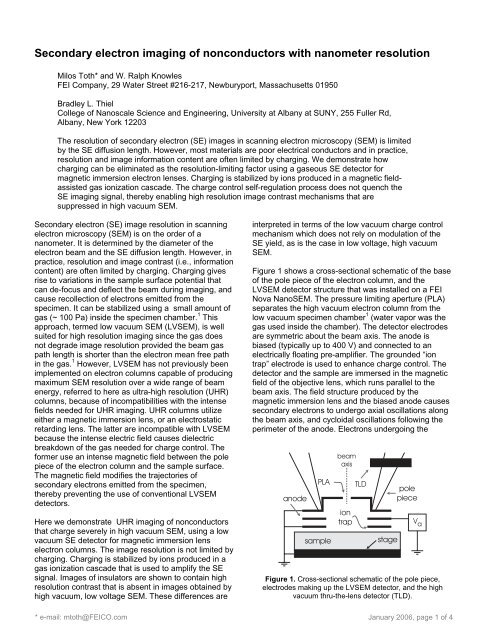
Figure 1 shows a cross-sectional schematic of the base<br />
of the pole piece of the electron column, and the<br />
LVSEM detector structure that was installed on a <strong>FEI</strong><br />
Nova NanoSEM. The pressure limiting aperture (PLA)<br />
separates the high vacuum electron column from the<br />
low vacuum specimen chamber 1 (water vapor was the<br />
gas used inside the chamber). The detector electrodes<br />
are symmetric about the beam axis. The anode is<br />
biased (typically up to 400 V) and connected to an<br />
electrically floating pre-amplifier. The grounded “ion<br />
trap” electrode is used to enhance charge control. The<br />
detector and the sample are immersed in the magnetic<br />
field of the objective lens, which runs parallel to the<br />
beam axis. The field structure produced by the<br />
magnetic immersion lens and the biased anode causes<br />
secondary electrons to undergo axial oscillations along<br />
the beam axis, and cycloidal oscillations following the<br />
perimeter of the anode. Electrons undergoing the<br />
anode<br />
PLA<br />
sample<br />
beam<br />
axis<br />
ion<br />
trap<br />
TLD<br />
stage<br />
pole<br />
piece<br />
Figure 1. Cross-sectional schematic of the pole piece,<br />
electrodes making up the LVSEM detector, and the high<br />
vacuum thru-the-lens detector (TLD).<br />
* e-mail: mtoth@<strong>FEI</strong>CO.com January 2006, page 1 of 4<br />
V a
oscillatory motion collide with gas molecules and give<br />
rise to a gas ionization cascade that amplifies the SE<br />
signal, and generates gaseous ions used for charge<br />
control. Detailed analyses of electron trajectories, and<br />
the gas cascade process are presented elsewhere. 2<br />
Figure 2 shows high resolution images of: (a, b) a<br />
chrome-on-quartz photomask, (c) a contact hole in<br />
Si3N4, and (d) a pit in SiO2 produced by an electrostatic<br />
discharge induced by a focused ion beam (in figure<br />
captions, P = gas pressure inside the specimen<br />
chamber and V0 = electron beam accelerating voltage).<br />
The photomask consists of microscopic, electrically<br />
floating pieces of an optical absorber on a macroscopic,<br />
6.25 mm tall quartz substrate. The absorber is<br />
identifiable by the grain structure clearly visible in both<br />
images. It consists of a 10 nm thick chrome oxide antireflective<br />
coating and a 90 nm chrome underlayer. In<br />
the high vacuum environments of conventional SEM<br />
and focused ion beam (FIB) tools, photomask imaging,<br />
metrology and repair are inhibited by severe<br />
charging. 3, 4 The low vacuum SE images in Figure 2 do<br />
not show charging artifacts. The resolution of the<br />
elevated magnification image in 2(b) is approximately<br />
1 nm (it was measured by detecting all edges in the<br />
image, and calculating the average distance over which<br />
the imaging signal rises, across an edge, from 30% to<br />
70% of the maximum intensity at each edge). The<br />
resolution is the same as in images of conductive goldon-carbon<br />
resolution standards obtained by high<br />
vacuum SEM, demonstrating that it is limited by<br />
electron optical aberrations (i.e., beam diameter) rather<br />
than charging.<br />
Images of the dielectrics shown in Figure 2(c) and (d)<br />
have a reduced resolution, in the range of 2-6 nm.<br />
These values probably correspond to the SE diffusion<br />
Figure 2. Low vacuum secondary electron images of: (a, b)<br />
chrome-on-quartz photolithographic mask [P = 100 Pa,<br />
V0 = 17 kV], (c) contact hole in Si3N4 [P = 100 Pa, V0 = 4 kV],<br />
(d) electrostatic discharge pit in SiO2 [P = 40 Pa, V0 = 7 kV].<br />
length, which places a fundamental limit on SE<br />
resolution. In insulators, the mean free paths (and<br />
hence the diffusion lengths) of low energy electrons are<br />
generally longer than in metals, due to the absence of<br />
electron-electron scattering at SE energies below the<br />
threshold for electron excitation across the bandgap.<br />
Hence, in insulators, SE diffusion is expected to limit<br />
resolution to an extent that is greater than in metals. 7<br />
Exact effects on images will depend on the contrast<br />
mechanism (e.g., variations in the SE generation rate or<br />
the height of the surface barrier) and feature proximity<br />
to other features in the image.<br />
We now turn to the topic of charging. Stable, high<br />
resolution imaging of nonconductors requires a charge<br />
control mechanism that does not rely on modulation of<br />
the electron beam landing energy, or the SE emission<br />
current. In low vacuum SEM, charging is stabilized by<br />
ions generated in the gas cascade which is used to<br />
amplify the imaging signal. 1 To illustrate the nature of<br />
low vacuum charge control, Figure 3 shows SE images<br />
of a pit in SiO2, obtained using: (a, b) the high vacuum<br />
thru-the-lens detector (TLD) and (c, d) the low vacuum<br />
detector shown in Figure 1. Images a and b were<br />
acquired using an accelerating voltage of 750 V,<br />
selected so as to minimize charging using the<br />
procedure described in Joy & Joy (1996) 8 . A number of<br />
features are marked on the images: (1) a defocused<br />
edge in the middle of a high vacuum image, and (2-3)<br />
SE contrast that is present in low vacuum images only.<br />
To interpret these features, we turn to models of charge<br />
balance in high and low vacuum SEM.<br />
The principle of charge conservation yields Equation 1,<br />
which must be satisfied at all times 5<br />
dq<br />
Ib = ( + δ ) Ib<br />
+ I S +<br />
dt<br />
η . (1)<br />
Figure 3. Secondary electron images of a pit in SiO2 obtained<br />
by: (a, b) high vacuum, low voltage SEM, and (c, d) low<br />
vacuum SEM [P = 50 Pa]<br />
5, 6<br />
January 2006, page 2 of 4
Ib and Is are the beam and specimen leakage current, η<br />
and δ are the backscattered and secondary electron<br />
yield, and dq/dt is the charge accumulation rate in the<br />
sample. In high vacuum SEM, dq/dt has a positively<br />
charged component corresponding to the holes left<br />
behind by SE emission, and a negative component<br />
corresponding to injected primary electrons 5<br />
+<br />
dq<br />
= −δI<br />
b , (2)<br />
dt<br />
−<br />
dq<br />
= 1 −η<br />
I . (3)<br />
dt<br />
( ) b<br />
In the case of bulk insulators, Is ≈ 0. Hence, in the<br />
steady state (denoted by ∞), dq/dt must be zero, and (in<br />
high vacuum SEM) 5<br />
0 = ( 1 −η<br />
∞ − δ ∞ ) I b , (4)<br />
∴δ ∞ = 1 −η∞<br />
. (5)<br />
That is, in high vacuum SEM, steady state is attained<br />
by modulation of δ (since, at the low beam energies<br />
needed for high vacuum imaging of insulators, 8 the<br />
initial and steady state values of η are approximately<br />
equal: η∞ ≈ ηt=0). SE yield modulation occurs through<br />
two mechanisms: 5 (i) recollection of emitted<br />
secondaries by a net positive sample surface, and (ii)<br />
lowering of the electron beam landing energy by a net<br />
negative specimen surface. Both of these mechanisms<br />
give rise to imaging artifacts. The former lowers the SE<br />
imaging signal, and can quench image contrast, as is<br />
discussed below. The latter can generate electric fields<br />
that are sufficiently intense to defocus and deflect the<br />
electron beam. Low voltage SEM 8 aims to minimize<br />
such fields by setting the electron beam accelerating<br />
voltage so as to yield the steady state landing energy in<br />
the presence of a negligible surface potential. However,<br />
in general, the critical landing energy varies from point<br />
to point across the sample surface, thereby giving rise<br />
to artifacts such as feature 1 in Figure 3(a) (i.e., a<br />
defocused, distorted edge in the middle of an otherwise<br />
focused image).<br />
Equation 5 implies that the steady state SE yield (δ∞) is<br />
a function of η∞ only. That is, all high resolution (“type<br />
1”) 7 SE contrast is generated during the transition from<br />
the initial to the steady state. The time constant<br />
associated with this transition is short relative to the<br />
pixel dwell times employed in SEM. 5 Hence, in high<br />
vacuum SEM images of insulators, the magnitude of the<br />
type 1 SE image component is low, and can not be<br />
increased by reducing the scan speed. This may<br />
explain the flat, featureless appearance of the high<br />
vacuum images shown in Figure 3(a) and (b) (relative to<br />
the corresponding low vacuum images c and d).<br />
Specifically, contrast within features 2 and 3 (indicated<br />
on Figure 3) is visible in low vacuum SE images only.<br />
The presence of such contrast in LVSEM images is<br />
discussed below.<br />
In low vacuum SEM, positive gas ions neutralize (and<br />
hence generate holes) at the sample surface. 9 Hence,<br />
dq + /dt has a component corresponding to the ion<br />
neutralization current (Ii)<br />
+<br />
dq<br />
= −δ<br />
I − I . (6)<br />
dt<br />
b<br />
i<br />
In the steady state (where dq/dt = 0) the sum of<br />
Equations 3 and 6 (i.e., the two components making up<br />
dq/dt) yields<br />
( − )<br />
Ii∞ δ ∞ = 1 η∞<br />
− . (7)<br />
Ib<br />
This expression indicates that, in low vacuum SEM, the<br />
steady state can be attained by modulation of II instead<br />
of δ. Hence, high resolution, (type 1) SE contrast is<br />
clearly visible in low vacuum images of insulators, as is<br />
illustrated by features 2 and 3 marked on Figures 3(d-f).<br />
We note that this contrast does not correspond to subsurface<br />
features located below the maximum<br />
penetration depth of the low energy (750 eV) electrons<br />
used to generate the images shown in Figures 3(a-b).<br />
The resolution of contrast generated by features below<br />
the SE escape depth is limited by beam spread below<br />
the sample surface. The resolution within features 2<br />
and 3 is on the order of the SE escape depth in<br />
insulators, which is much shorter than the penetration<br />
depth of the high energy (4 keV) electrons used to take<br />
the LVSEM images shown in Figures 3d-f.<br />
To achieve stable, artifact-free charge control, Ii must<br />
self-regulate as the beam is scanned across regions of<br />
samples exhibiting different charging behavior (e.g., the<br />
chrome-quartz interface or the pit shown in Figure 2(b)<br />
and 3(d), respectively). Ii can be made to self-regulate<br />
by making the fraction of ions reaching the specimen<br />
surface strongly dependent on the surface<br />
potential. 10, 11 This is achieved using the ion trap<br />
electrode shown in Figure 1, which acts as a sink of<br />
excess ions produced in the gas cascade (the high gas<br />
gains of 10 2 – 10 3 provide a source of excess ions<br />
inside the detector volume 2 ).<br />
In conclusion, we demonstrated that magnetic<br />
immersion lens LVSEM can eliminate specimen<br />
charging as the resolution-limiting factor in secondary<br />
electron imaging. Low vacuum secondary electron<br />
images can contain high resolution contrast that is<br />
absent in high vacuum, low voltage SEM, due to<br />
differences between charge control self-regulation<br />
mechanisms in low and high vacuum SEM.<br />
References<br />
1. B.L. Thiel and M. Toth, Secondary electron contrast<br />
in low-vacuum/environmental scanning electron<br />
microscopy of dielectrics. J. Appl. Phys. 97(5),<br />
051101 (2005).<br />
2. B.L. Thiel, M. Toth, R. Schroemges, H. Scholtz, G.<br />
van Veen and W.R. Knowles, A Two-Stage Gas<br />
Amplifier for Ultra-High Resolution Low-<br />
January 2006, page 3 of 4
Vacuum Scanning Electron Microscopy.<br />
Review of Scientific Instruments, in press<br />
(2006).<br />
3. M.T. Postek and A.E. Vladar, New application of<br />
variable-pressure/environmental microscopy to<br />
semiconductor inspection and metrology.<br />
Scanning 26(1), 11-17 (2004).<br />
4. M.T. Postek, A.E. Vladar and M.H. Bennett,<br />
Photomask dimensional metrology in the<br />
scanning electron microscope, part I: Has<br />
anything really changed. J. Microlithogr.<br />
Microfabr. Microsyst. 3(2), 212-223 (2004).<br />
5. J. Cazaux, Charging in scanning electron microscopy<br />
"from inside and outside". Scanning 26(4), 181-<br />
203 (2004).<br />
6. A. Howie, Threshold energy effects in secondary<br />
electron emission. Microsc. microanal. 6(4),<br />
291-296 (2000).<br />
7. H. Seiler, Secondary-Electron Emission In The<br />
Scanning Electron-Microscope. J. Appl. Phys.<br />
54(11), R1-R18 (1983).<br />
8. D.C. Joy and C.S. Joy, Low voltage scanning<br />
electron microscopy. Micron 27(3-4), 247-263<br />
(1996).<br />
9. M. Toth, M.R. Phillips, B.L. Thiel and A.M. Donald,<br />
Electron imaging of dielectrics under<br />
simultaneous electron-ion irradiation. J. Appl.<br />
Phys. 91(7), 4479-4491 (2002).<br />
10. J.P. Craven, F.S. Baker, B.L. Thiel and A.M.<br />
Donald, Consequences of positive ions upon<br />
imaging in low vacuum scanning electron<br />
microscopy. J. Microsc.-Oxf. 205, 96-105<br />
(2002).<br />
11. M. Toth, M.R. Phillips, J.P. Craven, B.L. Thiel and<br />
A.M. Donald, Electric fields produced by<br />
electron irradiation of insulators in a low<br />
vacuum environment. J. Appl. Phys. 91(7),<br />
4492-4499 (2002).<br />
January 2006, page 4 of 4