b - FEI Company
b - FEI Company
b - FEI Company

You also want an ePaper? Increase the reach of your titles
YUMPU automatically turns print PDFs into web optimized ePapers that Google loves.
oscillatory motion collide with gas molecules and give<br />
rise to a gas ionization cascade that amplifies the SE<br />
signal, and generates gaseous ions used for charge<br />
control. Detailed analyses of electron trajectories, and<br />
the gas cascade process are presented elsewhere. 2<br />
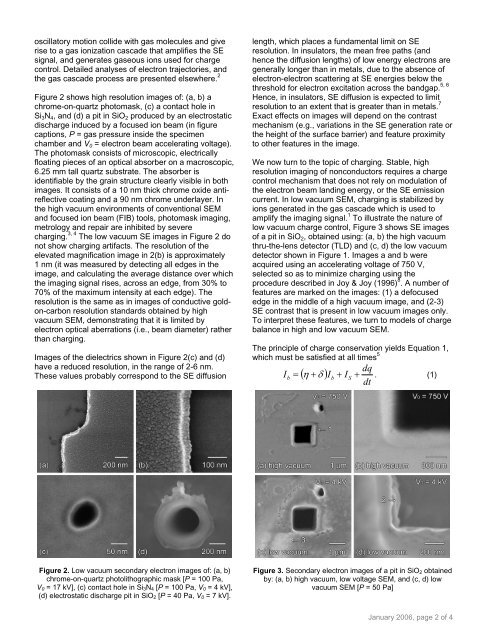
Figure 2 shows high resolution images of: (a, b) a<br />
chrome-on-quartz photomask, (c) a contact hole in<br />
Si3N4, and (d) a pit in SiO2 produced by an electrostatic<br />
discharge induced by a focused ion beam (in figure<br />
captions, P = gas pressure inside the specimen<br />
chamber and V0 = electron beam accelerating voltage).<br />
The photomask consists of microscopic, electrically<br />
floating pieces of an optical absorber on a macroscopic,<br />
6.25 mm tall quartz substrate. The absorber is<br />
identifiable by the grain structure clearly visible in both<br />
images. It consists of a 10 nm thick chrome oxide antireflective<br />
coating and a 90 nm chrome underlayer. In<br />
the high vacuum environments of conventional SEM<br />
and focused ion beam (FIB) tools, photomask imaging,<br />
metrology and repair are inhibited by severe<br />
charging. 3, 4 The low vacuum SE images in Figure 2 do<br />
not show charging artifacts. The resolution of the<br />
elevated magnification image in 2(b) is approximately<br />
1 nm (it was measured by detecting all edges in the<br />
image, and calculating the average distance over which<br />
the imaging signal rises, across an edge, from 30% to<br />
70% of the maximum intensity at each edge). The<br />
resolution is the same as in images of conductive goldon-carbon<br />
resolution standards obtained by high<br />
vacuum SEM, demonstrating that it is limited by<br />
electron optical aberrations (i.e., beam diameter) rather<br />
than charging.<br />
Images of the dielectrics shown in Figure 2(c) and (d)<br />
have a reduced resolution, in the range of 2-6 nm.<br />
These values probably correspond to the SE diffusion<br />
Figure 2. Low vacuum secondary electron images of: (a, b)<br />
chrome-on-quartz photolithographic mask [P = 100 Pa,<br />
V0 = 17 kV], (c) contact hole in Si3N4 [P = 100 Pa, V0 = 4 kV],<br />
(d) electrostatic discharge pit in SiO2 [P = 40 Pa, V0 = 7 kV].<br />
length, which places a fundamental limit on SE<br />
resolution. In insulators, the mean free paths (and<br />
hence the diffusion lengths) of low energy electrons are<br />
generally longer than in metals, due to the absence of<br />
electron-electron scattering at SE energies below the<br />
threshold for electron excitation across the bandgap.<br />
Hence, in insulators, SE diffusion is expected to limit<br />
resolution to an extent that is greater than in metals. 7<br />
Exact effects on images will depend on the contrast<br />
mechanism (e.g., variations in the SE generation rate or<br />
the height of the surface barrier) and feature proximity<br />
to other features in the image.<br />
We now turn to the topic of charging. Stable, high<br />
resolution imaging of nonconductors requires a charge<br />
control mechanism that does not rely on modulation of<br />
the electron beam landing energy, or the SE emission<br />
current. In low vacuum SEM, charging is stabilized by<br />
ions generated in the gas cascade which is used to<br />
amplify the imaging signal. 1 To illustrate the nature of<br />
low vacuum charge control, Figure 3 shows SE images<br />
of a pit in SiO2, obtained using: (a, b) the high vacuum<br />
thru-the-lens detector (TLD) and (c, d) the low vacuum<br />
detector shown in Figure 1. Images a and b were<br />
acquired using an accelerating voltage of 750 V,<br />
selected so as to minimize charging using the<br />
procedure described in Joy & Joy (1996) 8 . A number of<br />
features are marked on the images: (1) a defocused<br />
edge in the middle of a high vacuum image, and (2-3)<br />
SE contrast that is present in low vacuum images only.<br />
To interpret these features, we turn to models of charge<br />
balance in high and low vacuum SEM.<br />
The principle of charge conservation yields Equation 1,<br />
which must be satisfied at all times 5<br />
dq<br />
Ib = ( + δ ) Ib<br />
+ I S +<br />
dt<br />
η . (1)<br />
Figure 3. Secondary electron images of a pit in SiO2 obtained<br />
by: (a, b) high vacuum, low voltage SEM, and (c, d) low<br />
vacuum SEM [P = 50 Pa]<br />
5, 6<br />
January 2006, page 2 of 4