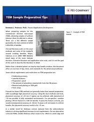
b - FEI Company
b - FEI Company
b - FEI Company

You also want an ePaper? Increase the reach of your titles
YUMPU automatically turns print PDFs into web optimized ePapers that Google loves.
Ib and Is are the beam and specimen leakage current, η<br />
and δ are the backscattered and secondary electron<br />
yield, and dq/dt is the charge accumulation rate in the<br />
sample. In high vacuum SEM, dq/dt has a positively<br />
charged component corresponding to the holes left<br />
behind by SE emission, and a negative component<br />
corresponding to injected primary electrons 5<br />
+<br />
dq<br />
= −δI<br />
b , (2)<br />
dt<br />
−<br />
dq<br />
= 1 −η<br />
I . (3)<br />
dt<br />
( ) b<br />
In the case of bulk insulators, Is ≈ 0. Hence, in the<br />
steady state (denoted by ∞), dq/dt must be zero, and (in<br />
high vacuum SEM) 5<br />
0 = ( 1 −η<br />
∞ − δ ∞ ) I b , (4)<br />
∴δ ∞ = 1 −η∞<br />
. (5)<br />
That is, in high vacuum SEM, steady state is attained<br />
by modulation of δ (since, at the low beam energies<br />
needed for high vacuum imaging of insulators, 8 the<br />
initial and steady state values of η are approximately<br />
equal: η∞ ≈ ηt=0). SE yield modulation occurs through<br />
two mechanisms: 5 (i) recollection of emitted<br />
secondaries by a net positive sample surface, and (ii)<br />
lowering of the electron beam landing energy by a net<br />
negative specimen surface. Both of these mechanisms<br />
give rise to imaging artifacts. The former lowers the SE<br />
imaging signal, and can quench image contrast, as is<br />
discussed below. The latter can generate electric fields<br />
that are sufficiently intense to defocus and deflect the<br />
electron beam. Low voltage SEM 8 aims to minimize<br />
such fields by setting the electron beam accelerating<br />
voltage so as to yield the steady state landing energy in<br />
the presence of a negligible surface potential. However,<br />
in general, the critical landing energy varies from point<br />
to point across the sample surface, thereby giving rise<br />
to artifacts such as feature 1 in Figure 3(a) (i.e., a<br />
defocused, distorted edge in the middle of an otherwise<br />
focused image).<br />
Equation 5 implies that the steady state SE yield (δ∞) is<br />
a function of η∞ only. That is, all high resolution (“type<br />
1”) 7 SE contrast is generated during the transition from<br />
the initial to the steady state. The time constant<br />
associated with this transition is short relative to the<br />
pixel dwell times employed in SEM. 5 Hence, in high<br />
vacuum SEM images of insulators, the magnitude of the<br />
type 1 SE image component is low, and can not be<br />
increased by reducing the scan speed. This may<br />
explain the flat, featureless appearance of the high<br />
vacuum images shown in Figure 3(a) and (b) (relative to<br />
the corresponding low vacuum images c and d).<br />
Specifically, contrast within features 2 and 3 (indicated<br />
on Figure 3) is visible in low vacuum SE images only.<br />
The presence of such contrast in LVSEM images is<br />
discussed below.<br />
In low vacuum SEM, positive gas ions neutralize (and<br />
hence generate holes) at the sample surface. 9 Hence,<br />
dq + /dt has a component corresponding to the ion<br />
neutralization current (Ii)<br />
+<br />
dq<br />
= −δ<br />
I − I . (6)<br />
dt<br />
b<br />
i<br />
In the steady state (where dq/dt = 0) the sum of<br />
Equations 3 and 6 (i.e., the two components making up<br />
dq/dt) yields<br />
( − )<br />
Ii∞ δ ∞ = 1 η∞<br />
− . (7)<br />
Ib<br />
This expression indicates that, in low vacuum SEM, the<br />
steady state can be attained by modulation of II instead<br />
of δ. Hence, high resolution, (type 1) SE contrast is<br />
clearly visible in low vacuum images of insulators, as is<br />
illustrated by features 2 and 3 marked on Figures 3(d-f).<br />
We note that this contrast does not correspond to subsurface<br />
features located below the maximum<br />
penetration depth of the low energy (750 eV) electrons<br />
used to generate the images shown in Figures 3(a-b).<br />
The resolution of contrast generated by features below<br />
the SE escape depth is limited by beam spread below<br />
the sample surface. The resolution within features 2<br />
and 3 is on the order of the SE escape depth in<br />
insulators, which is much shorter than the penetration<br />
depth of the high energy (4 keV) electrons used to take<br />
the LVSEM images shown in Figures 3d-f.<br />
To achieve stable, artifact-free charge control, Ii must<br />
self-regulate as the beam is scanned across regions of<br />
samples exhibiting different charging behavior (e.g., the<br />
chrome-quartz interface or the pit shown in Figure 2(b)<br />
and 3(d), respectively). Ii can be made to self-regulate<br />
by making the fraction of ions reaching the specimen<br />
surface strongly dependent on the surface<br />
potential. 10, 11 This is achieved using the ion trap<br />
electrode shown in Figure 1, which acts as a sink of<br />
excess ions produced in the gas cascade (the high gas<br />
gains of 10 2 – 10 3 provide a source of excess ions<br />
inside the detector volume 2 ).<br />
In conclusion, we demonstrated that magnetic<br />
immersion lens LVSEM can eliminate specimen<br />
charging as the resolution-limiting factor in secondary<br />
electron imaging. Low vacuum secondary electron<br />
images can contain high resolution contrast that is<br />
absent in high vacuum, low voltage SEM, due to<br />
differences between charge control self-regulation<br />
mechanisms in low and high vacuum SEM.<br />
References<br />
1. B.L. Thiel and M. Toth, Secondary electron contrast<br />
in low-vacuum/environmental scanning electron<br />
microscopy of dielectrics. J. Appl. Phys. 97(5),<br />
051101 (2005).<br />
2. B.L. Thiel, M. Toth, R. Schroemges, H. Scholtz, G.<br />
van Veen and W.R. Knowles, A Two-Stage Gas<br />
Amplifier for Ultra-High Resolution Low-<br />
January 2006, page 3 of 4