Chapter 4 Digital Logic and Implementation 4.1 Boolean Algebra
Chapter 4 Digital Logic and Implementation 4.1 Boolean Algebra
Chapter 4 Digital Logic and Implementation 4.1 Boolean Algebra

Create successful ePaper yourself
Turn your PDF publications into a flip-book with our unique Google optimized e-Paper software.
<strong>Chapter</strong> 4<br />
<strong>Digital</strong> <strong>Logic</strong> <strong>and</strong> <strong>Implementation</strong><br />
<strong>4.1</strong> <strong>Boolean</strong> <strong>Algebra</strong><br />
<strong>4.1</strong>.1 <strong>Boolean</strong> logic<br />
• A single bit can be either 0 or 1. You can interpret 0 as the logical value false <strong>and</strong><br />
1 as the logical value true. In this way, a bit stored in the memory of a computer can<br />
represent a logical value that is either false or true.<br />
• The digital computer is based on <strong>Boolean</strong> logic or <strong>Boolean</strong> algebra.<br />
• There are a number of logical rules, but these can all be derived from three fundamental<br />
operations, the operations of AND, OR, <strong>and</strong> NOT, which are called fundamental logical<br />
operations<br />
• If you interpret a bit as a logical value, then you can apply logical operations on this bit.<br />
Operations AND <strong>and</strong> OR are binary operations which accept 2 bit inputs to create only<br />
1 bit output, while the operation NOT is a unary operation.<br />
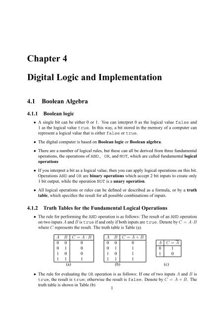
• All logical operations or rules can be defined or described as a formula, or by a truth<br />
table, which specifies the result for all possible combinations of inputs.<br />
<strong>4.1</strong>.2 Truth Tables for the Fundamental <strong>Logic</strong>al Operations<br />
• The rule for performing the AND operation is as follows: The result of an AND operation<br />
on two inputs A <strong>and</strong> B is true if <strong>and</strong> only if both inputs are true. Denote by C = A·B<br />
where C represents the result. The truth table is Table (a)<br />
A B C = A · B<br />
0 0 0<br />
0 1 0<br />
1 0 0<br />
1 1 1<br />
A B C = A + B<br />
0 0 0<br />
0 1 1<br />
1 0 1<br />
1 1 1<br />
A C = A<br />
0 1<br />
1 0<br />
(a) (b) (c)<br />
• The rule for evaluating the OR operation is as follows: If one of two inputs A <strong>and</strong> B is<br />
true, the result is true; otherwise the result is false. Denote by C = A + B. The<br />
truth table is shown in Table (b)<br />
1
2 CHAPTER 4. DIGITAL LOGIC AND IMPLEMENTATION<br />
• The rule for evaluating the NOT operation is as follows: If the input A is true, the result<br />
is false, <strong>and</strong> if the input is false, the result is true. The truth table is shown in<br />
Table (c).<br />
• With three fundamental operations you can make up other operations or <strong>Boolean</strong> expressions.<br />
For example, the Exclusive-OR operation is defined as<br />
C = A ⊕ b = (A + B) · A · B<br />
It is easy for you to construct the truth table for the exclusive-or operation.<br />
<strong>4.1</strong>.3 <strong>Logic</strong> Laws<br />
• There are a number of useful laws <strong>and</strong> identities that help to manipulate <strong>Boolean</strong> equations.<br />
• <strong>Boolean</strong> algebra operations are associative, distributive, <strong>and</strong> communicative<br />
A + B = B + A<br />
A + (B + C) = (A + B) + C,<br />
A · (B + C) = A · B + A · C<br />
A · B = B · A<br />
A · (B · C) = (A · B) · C<br />
• DeMorgan’s Law<br />
A + B = A · B <strong>and</strong> A · B = A + B<br />
• It is easy for you to prove these laws using their truth table. The method is to show the<br />
truth tables of both sides of the equation are same. Let us prove that A · B = A + B.<br />
For the left side, using the truth tables of the three fundamental operations we have<br />
A B A · B A · B<br />
0 0 0 1<br />
0 1 0 1<br />
1 0 0 1<br />
1 1 1 0<br />
For the right side, we have<br />
A B A B A + B<br />
0 0 1 1 1<br />
0 1 1 0 1<br />
1 0 0 1 1<br />
1 1 0 0 0<br />
You can see the column A · B in the first truth table is exactly same as the column A + B<br />
in the second truth table. That is, for each pair of inputs A <strong>and</strong> B, the values from A · B<br />
<strong>and</strong> A + B are same. Hence A · B = A + B
4.2. LOGIC GATES 3<br />
4.2 <strong>Logic</strong> Gates<br />
4.2.1 Three Fundamental Gates<br />
• A gate is an electronic device that operates on a collection of binary inputs to produce a<br />
binary output. Gates are constructed from transistor switches <strong>and</strong> other electronic components,<br />
formed into integrated circuits.<br />
• Gates can implement a wide range of different logical rules, eps., the three fundamental<br />
logical operations.<br />
• The following Figure shows the diagram of circuits constructing the NOT operation. In<br />
the diagram, the collector of the transistor is connected to the power supply <strong>and</strong> the<br />
emitter is grounded. If the control line is set to 1, then the transistor is in the ON state,<br />
<strong>and</strong> it passes the current through to the ground. In this case, the output of the gate is<br />
0. However, if the control line is set to 0, the transistor is the OFF state, <strong>and</strong> it blocks<br />
passage of the current to the ground. Instead, the current is transmitted to the output line,<br />
producing an output of 1. Thus if we consider the control line as the input of a logical<br />
rule, <strong>and</strong> the output line as the output of the rule, then this circuit behaves exactly same<br />
as the NOT operation. We call this gate as the NOT gate.<br />
Power Supply<br />
¡<br />
¡<br />
Collector<br />
Output<br />
Line<br />
Control<br />
Emitter<br />
(Grounded)<br />
• Similarly we can construct gates for OR, NOT <strong>and</strong> Exclusive-OR operations.<br />
• Here are the st<strong>and</strong>ard logic gate representations for the fundamental logic operations.<br />
4.2.2 Combinatorial <strong>Logic</strong> Circuits<br />
• It is not difficult to manipulate the <strong>Boolean</strong> algebra to show that combinatorial <strong>Boolean</strong><br />
logic can be implemented entirely with a series of fundamental gates. For more examples<br />
see Figure S1.8 <strong>and</strong> S1.9 on page 653 of the textbook.
4 CHAPTER 4. DIGITAL LOGIC AND IMPLEMENTATION<br />
• Figure S1.10 shows a circuit called a selector. It can be used to switch the input between<br />
A <strong>and</strong> B depending on the signal from the select line. You can use this simple selector to<br />
build up a selector between two bytes of data, or more.<br />
• The half adder shown in Figure S1.11 is another interesting combinatorial logic circuits.<br />
If you review the addition table for binary numbers, you will note that 0+0 = 0, 1+0 = 1,<br />
0 + 1 = 1 (without carries, considered as 0) <strong>and</strong> 1 + 1 = 10 ( with a carry 1). We can<br />
split the addition into two parts:<br />
– The sum part (S), (0, 0) → 0, (0, 1) → 1, (1, 0) → 1 <strong>and</strong> (1, 1) → 0 which can be<br />
described by the Exclusive-OR operation<br />
– The carry part (C), (0, 0) → 0, (0, 1) → 0, (1, 0) → 0 <strong>and</strong> (1, 1) → 1 which can be<br />
described by the AND operation.<br />
Combining two parts together results in a half adder. Figure S1.11 shows one of such<br />
examples.<br />
• In the addition of binary numbers, you must consider the carries from the previous bits.<br />
To implement binary addition by circuits, you must include carries in the operation. Figure<br />
S1.12 shows the so-called full adder in which two half adders are connected together<br />
to cope with the carry from the previous bit. In the circuit, the previous carry is added to<br />
the sum part. This addition may create another carry. Finally two possible carries are put<br />
into a NAND gate to generate the final carry (why?).<br />
• A full adder calculates one bit addition with possible carry from the previous bit. You<br />
can combine a series of full adder circuits to make a large circuit for the addition of two<br />
binary numbers with more bits.<br />
4.2.3 Sequential <strong>Logic</strong> Circuits<br />
• Sequential logic circuits are circuits whose output is dependent not only on the input <strong>and</strong><br />
the circuit configuration, but also on the previous state of the circuit.<br />
• The key to sequential logic circuit is the presence of memory within the circuit. The state<br />
of the circuit is stored in these memory bits.<br />
• The basic memory element in a sequential logic circuit is called a flip-flop. The simplest<br />
flip-flop is shown in Figure S1.13.<br />
• There are many other types of flip-flop circuits. They are used to construct some control<br />
circuits in a computer. This is beyond our course.<br />
4.3 Application <strong>and</strong> <strong>Implementation</strong><br />
4.3.1 A Compare-For-Equality Circuit<br />
• The first example is the compare-for-equality circuit, or CE circuit, which tests two unsigned<br />
binary numbers for exact equality, i.e., all the corresponding bits are equal.
4.3. APPLICATION AND IMPLEMENTATION 5<br />
• First we consider the compare-for-equality for a single bit. The comparison operation<br />
here is defined by<br />
A B The Result of Comparison<br />
0 0 1<br />
1 0 0<br />
0 1 0<br />
1 1 1<br />
This task can be fulfilled by the Exclusive-OR gate.<br />
• Suppose the binary numbers have N bits (generally N is 8 or 16 or 32 etc). Denote A =<br />
a N−1 a N−2 ...a 0 <strong>and</strong> B = b N−1 b N−2 ...b 0 . For each pair (a i , b i ), we use a Exclusive-OR<br />
gate to compare it. Thus we have N outputs (one per bit).<br />
• Group the outputs subgroups of 2 outputs, <strong>and</strong> connect them into a AND gate. There will<br />
be N/2 AND gates. Group them successively in the same way until we have only one<br />
output which gives the result of comparison between two binary numbers.<br />
4.3.2 An Addition Circuit<br />
• The full adder is the circuit for the addition of two bits. You can use it to construct a full<br />
addition circuit for two binary numbers with N bits.<br />
• Mathematically the addition is defined as<br />
• The full addition circuit is<br />
a N−1 a N−2 a N−3 · · · a 0<br />
+ b N−1 b N−2 b N−3 · · · b 0<br />
s N s N−1 s N−2 s N−3 · · · s 0<br />
N−bit input value b<br />
b N−1<br />
b N−2<br />
. . . b 1<br />
b 0<br />
N−bit input value a<br />
a<br />
N−1<br />
a a<br />
1<br />
a<br />
0<br />
N−2 . . .<br />
C C C C C<br />
Initial<br />
N 1−ADD N−1 1−ADD N−2 . . . . 2 1−ADD 2 1−ADD Carry 0<br />
. . . . . .<br />
S N SN−1 SN−2 S 1 S 0<br />
(N+1)−bit output value S<br />
where c i represents the carry output from a full adder <strong>and</strong> the initial carry is set to 0 (no<br />
carry at all)

![Question 1 [22 Marks] In the 1974 Motor Trend US magazine, fuel ...](https://img.yumpu.com/27496340/1/190x245/question-1-22-marks-in-the-1974-motor-trend-us-magazine-fuel-.jpg?quality=85)