Service Repair Documentation Level 2.5e – HIT ... - Altehandys.de
Service Repair Documentation Level 2.5e – HIT ... - Altehandys.de
Service Repair Documentation Level 2.5e – HIT ... - Altehandys.de

You also want an ePaper? Increase the reach of your titles
YUMPU automatically turns print PDFs into web optimized ePapers that Google loves.
Company Confi<strong>de</strong>ntial<br />
Copyright 2004© Siemens AG<br />
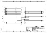
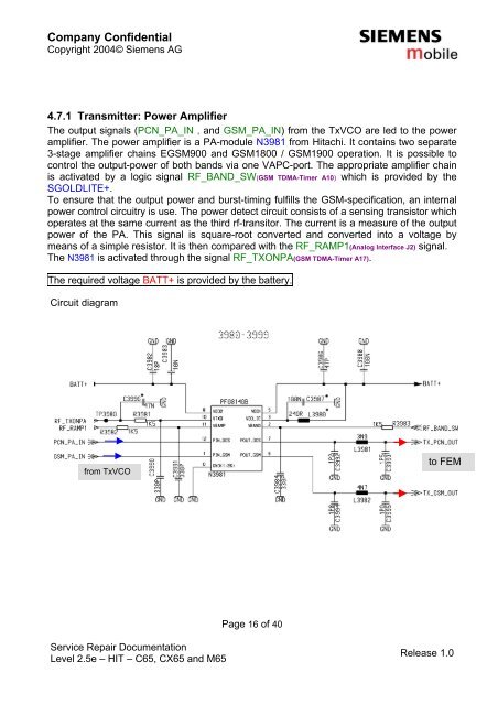
4.7.1 Transmitter: Power Amplifier<br />
The output signals (PCN_PA_IN , and GSM_PA_IN) from the TxVCO are led to the power<br />
amplifier. The power amplifier is a PA-module N3981 from Hitachi. It contains two separate<br />
3-stage amplifier chains EGSM900 and GSM1800 / GSM1900 operation. It is possible to<br />
control the output-power of both bands via one VAPC-port. The appropriate amplifier chain<br />
is activated by a logic signal RF_BAND_SW(GSM TDMA-Timer A10) which is provi<strong>de</strong>d by the<br />
SGOLDLITE+.<br />
To ensure that the output power and burst-timing fulfills the GSM-specification, an internal<br />
power control circuitry is use. The power <strong>de</strong>tect circuit consists of a sensing transistor which<br />
operates at the same current as the third rf-transitor. The current is a measure of the output<br />
power of the PA. This signal is square-root converted and converted into a voltage by<br />
means of a simple resistor. It is then compared with the RF_RAMP1(Analog Interface J2) signal.<br />
The N3981 is activated through the signal RF_TXONPA(GSM TDMA-Timer A17).<br />
The required voltage BATT+ is provi<strong>de</strong>d by the battery.<br />
Circuit diagram<br />
from TxVCO<br />
<strong>Service</strong> <strong>Repair</strong> <strong>Documentation</strong><br />
<strong>Level</strong> <strong>2.5e</strong> <strong>–</strong> <strong>HIT</strong> <strong>–</strong> C65, CX65 and M65<br />
Page 16 of 40<br />
to FEM<br />
Release 1.0