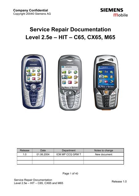
Service Repair Documentation Level 2.5e – HIT ... - Altehandys.de
Service Repair Documentation Level 2.5e – HIT ... - Altehandys.de
Service Repair Documentation Level 2.5e – HIT ... - Altehandys.de

You also want an ePaper? Increase the reach of your titles
YUMPU automatically turns print PDFs into web optimized ePapers that Google loves.
Company Confi<strong>de</strong>ntial<br />
Copyright 2004© Siemens AG<br />
<strong>Service</strong> <strong>Repair</strong> <strong>Documentation</strong><br />
<strong>Level</strong> <strong>2.5e</strong> <strong>–</strong> <strong>HIT</strong> <strong>–</strong> C65, CX65, M65<br />
Release Date Department Notes to change<br />
1.0 01.06.2004 ICM MP CCQ GRM T New document<br />
<strong>Service</strong> <strong>Repair</strong> <strong>Documentation</strong><br />
<strong>Level</strong> <strong>2.5e</strong> <strong>–</strong> <strong>HIT</strong> <strong>–</strong> C65, CX65 and M65<br />
Page 1 of 40<br />
Release 1.0
Company Confi<strong>de</strong>ntial<br />
Copyright 2004© Siemens AG<br />
Table of Contents:<br />
1 List of available level 2,5e parts C65, CX65, M65 ........................................................3<br />
2 Required Equipment for <strong>Level</strong> 2,5e...............................................................................4<br />
3 Required Software for <strong>Level</strong> 2,5e C65, CX65, M65 ......................................................4<br />
4 Radio Part.....................................................................................................................5<br />
5 Logic / Control.............................................................................................................18<br />
6 Power Supply..............................................................................................................25<br />
7 Camera .......................................................................................................................28<br />
8 Camera <strong>–</strong> Display Interface Module............................................................................28<br />
9 Display Modules..........................................................................................................30<br />
10 Illumination..................................................................................................................32<br />
11 Interfaces ....................................................................................................................34<br />
12 Keyboard ....................................................................................................................40<br />
<strong>Service</strong> <strong>Repair</strong> <strong>Documentation</strong><br />
<strong>Level</strong> <strong>2.5e</strong> <strong>–</strong> <strong>HIT</strong> <strong>–</strong> C65, CX65 and M65<br />
Page 2 of 40<br />
Release 1.0
Company Confi<strong>de</strong>ntial<br />
Copyright 2004© Siemens AG<br />
1 List of available level 2,5e parts C65, CX65, M65<br />
Component Typ/Circuit Part Mobile Phone Component Details ID Partnumber<br />
ASIC C65, M65 Camera Interface_S1D13716B02<br />
Power Supply D1094DA<br />
D3601 L36820-U6054-D670<br />
ASIC C65, CX65, M65 MOZART_TWIGO4 D1300 L36145-J4683-Y19<br />
ASIC CX65 Camera Interface_S1D13716B01 D3601 L36820-U6052-D670<br />
Cap_Dio<strong>de</strong>_26MHz_Circuit C65, CX65, M65 Cap_Dio<strong>de</strong>_1SV305 V3961 L36840-D61-D670<br />
Capacitor_Camera_Circuit CX65, M65 Capacitor 2*2U2 C3609 L36344-F1225-M12<br />
Capacitor_Mozart_Twigo_Circuit C65, CX65, M65 Capacitor 2*2U2 C1304 L36344-F1225-M12<br />
Capacitor_Mozart_Twigo_Circuit C65, CX65, M65 Capacitor 2*2U2 C1315 L36344-F1225-M12<br />
Capacitor_Mozart_Twigo_Circuit C65, CX65, M65 Capacitor 2*2U2 C1318 L36344-F1225-M12<br />
Capacitor_Mozart_Twigo_Circuit C65, CX65, M65 Capacitor 2*2U2 C1329 L36344-F1225-M12<br />
Capacitor_Mozart_Twigo_Circuit C65, CX65, M65 Capacitor 2*2U2 C1330 L36344-F1225-M12<br />
Capacitor_Mozart_Twigo_Circuit C65 Capacitor 2*2U2 C1331 L36344-F1225-M12<br />
Capacitor_Mozart_Twigo_Circuit C65, CX65, M65 Capacitor 2*2U2 C1332 L36344-F1225-M12<br />
Coil_BATT+ C65, CX65, M65 Coil BKP1608HS391 L1300 L36140-F2100-Y6<br />
Coil_BATT+ C65, CX65, M65 Coil BKP1608HS391 L1318 L36140-F2100-Y6<br />
Coil_VBOOST C65, CX65, M65 Coil BKP1608HS391 L1331 L36140-F2100-Y6<br />
Coil_VBOOST C65, CX65, M65 Coil 4U7 L1302 L36151-F5472-M1<br />
Coil_VBUCK C65, CX65, M65 Coil 10U L1301 L36151-F5103-M3<br />
Dio<strong>de</strong>_Battery_Interface C65, CX65, M65 Dio<strong>de</strong> BAV99T V1400 L36840-D66-D670<br />
Dio<strong>de</strong>_SIM_Circuit C65, CX65, M65 Dio<strong>de</strong> ZENER EMZ6.8E V1605 L36840-D3088-D670<br />
Dio<strong>de</strong>_VBOOST C65, CX65, M65 Dio<strong>de</strong> BAT760 V1303 L36840-D5076-D670<br />
Dio<strong>de</strong>_VBUCK C65, CX65, M65 Dio<strong>de</strong> BAT760 V1302 L36840-D5076-D670<br />
Dio<strong>de</strong>_Vibra_Circuit CX65, M65 Dio<strong>de</strong> BAV99T V2100 L36840-D66-D670<br />
Filter_IO Interface C65, CX65, M65 EMI_EMV_Filter_IP4559CX25 Z1500 L36820-L6147-D670<br />
IC MODUL PA C65, CX65, M65 PF08140B SMD N3981 L36851-Z2002-A63<br />
IC_FEM C65, CX65, M65 FEM <strong>HIT</strong>ACHI GSM900 1800 1900 N3901 L36145-K280-Y258<br />
IC_Processor_SGOLDLITELITE C65, CX65, M65 PMB8875 V1X D1000 L36810-G6191-D670<br />
IC_Transceiver C65, CX65, M65 HD155155NPEB N3921 L36820-L6142-D670<br />
Oszillator_RF_Logic C65, CX65, M65 Oszillator_26MHz Z3961 L36145-F260-Y17<br />
Oszillator_RTC C65, CX65, M65 Oszillator_32,768KHZ Z1000 L36145-F102-Y21<br />
Resistor_Temp_TVCXO C65, CX65, M65 Resistor_Temp 22k R R3967 L36120-F4223-H<br />
Switch_USB C65, CX65, M65 NC7WB66K8X DUAL BUS SWITCH N1501 L36810-B6132-D670<br />
Trans_Charge_Circuit C65, CX65, M65 Transistor SI5933DC V1305 L36830-C1107-D670<br />
Trans_DISPLAY_BACKLIGHT C65, CX65, M65 Transistor EMB9/PEMB9 V2303 L36840-C4059-D670<br />
Trans_DISPLAY_BACKLIGHT C65 Transistor BC847BS BC846S V2302 L36840-C4061-D670<br />
Trans_DISPLAY_BACKLIGHT C65, CX65 Transistor BC847BS/BC846S V2821 L36840-C4061-D670<br />
Trans_DISPLAY_BACKLIGHT CX65, M65 Transistor BCS 46S V2302 L36840-C4014-D670<br />
Trans_DISPLAY_BACKLIGHT M65 Transistor FDG6303N SI1902DL V2821 L36830-C1112-D670<br />
Trans_NIGHT_DESIGN_LIGHT CX65, M65 Transistor FDG6303N SI1902DL V2404 L36830-C1112-D670<br />
Trans_V2.65V C65, CX65, M65 Transistor EMD12 V1500 L36840-C4057-D670<br />
Trans_VBOOST C65, CX65, M65 Transistor FDG313N V1304 L36830-C1121-D670<br />
Volt.Regulator_Camera C65 Volt.Reg. LP3985ITLX-2.9 N3600 L36810-C6134-D670<br />
Volt.Regulator_Camera CX65, M65 Volt.Reg. LP1986_2*2.85V N3600 L36810-C6065-D670<br />
<strong>Service</strong> <strong>Repair</strong> <strong>Documentation</strong><br />
<strong>Level</strong> <strong>2.5e</strong> <strong>–</strong> <strong>HIT</strong> <strong>–</strong> C65, CX65 and M65<br />
Page 3 of 40<br />
Release 1.0
Company Confi<strong>de</strong>ntial<br />
Copyright 2004© Siemens AG<br />
2 Required Equipment for <strong>Level</strong> 2,5e<br />
- GSM-Tester (CMU200 or 4400S incl. Options)<br />
- PC-incl. Monitor, Keyboard and Mouse<br />
- Bootadapter 2000/2002 (L36880-N9241-A200)<br />
- Adapter cable for Bootadapter due to new Lumberg connector (F30032-P226-A1)<br />
- Troubleshooting Frame C65 (F30032-P377-A1)<br />
- Troubleshooting Frame CX65, M65 (F30032-P343-A1)<br />
- Power Supply (at least one GRT required power supply)<br />
- Spectrum Analyser<br />
- Active RF-Probe incl. Power Supply<br />
- Oscilloscope incl. Probe<br />
- RF-Connector (NSMA(f))<br />
- Power Supply Cables<br />
- Dongle (F30032-P28-A1) if USB-Dongle is used a special driver for NT is required<br />
- BGA Sol<strong>de</strong>ring equipment<br />
Reference: Equipment recommendation Version X (newest version)<br />
(downloadable from the technical support page)<br />
3 Required Software for <strong>Level</strong> 2,5e C65, CX65, M65<br />
- Winsui for 65series<br />
- Software for GSM-Tester (GRT)<br />
- Software for reference oscillator adjustment<br />
- Internet unblocking solution (JPICS)<br />
- Dongle driver for dongle protected Siemens software tools<br />
<strong>Service</strong> <strong>Repair</strong> <strong>Documentation</strong><br />
<strong>Level</strong> <strong>2.5e</strong> <strong>–</strong> <strong>HIT</strong> <strong>–</strong> C65, CX65 and M65<br />
Page 4 of 40<br />
Release 1.0
Company Confi<strong>de</strong>ntial<br />
Copyright 2004© Siemens AG<br />
4 Radio Part<br />
The radio part realizes the conversion of the GMSK-HF-signals from the antenna to the<br />
base-band and vice versa.<br />
In the receiving direction, the signals are split in the I- and Q-component and led to the D/Aconverter<br />
of the logic part. In the transmission direction, the GMSK-signal is generated in an<br />
Up Conversion Modulation Phase Locked Loop by modulation of the I- and Q-signals which<br />
were generated in the logic part. After that the signals are amplified in the power amplifier.<br />
Transmitter and Receiver are never active at the same time. Simultaneous receiving in two<br />
bands is impossible. Simultaneous transmission in two bands is impossible, too. However<br />
the monitoring band (monitoring timeslot) in the TDMA-frame can be chosen in<strong>de</strong>pen<strong>de</strong>ntly<br />
of the receiving respectively the transmitting band (RX- and TX timeslot of the band).<br />
The RF-part of the C65, CX65 and M65 are dimensioned for triple band operation<br />
(EGSM900, GSM1800, GSM1900) supporting GPRS functionality up to multiclass 10.<br />
The RF-circuit consists of the following components:<br />
• Hitachi Bright VE chip set with the following functionality:<br />
o PLL for local oscillator LO1 and LO2 and TxVCO<br />
o Integrated local oscillators LO1, LO2 (without loop filter)<br />
o Integrated TxVCO (without loop filter and core inductors for GSM)<br />
o Direct conversion receiver including LNA, DC-mixer, channel filtering and PGCamplifier<br />
o Active part of 26 MHz reference oscillator<br />
• Hitachi LTCC transmitter power amplifier with integrated power control circuitry<br />
• Hitachi Frontend-Module including RX-/TX-switch and EGSM900 / GSM1800 / GSM<br />
1900 receiver SAW-filters<br />
Quartz and passive circuitry of the 26MHz VCXO reference oscillator.<br />
<strong>Service</strong> <strong>Repair</strong> <strong>Documentation</strong><br />
<strong>Level</strong> <strong>2.5e</strong> <strong>–</strong> <strong>HIT</strong> <strong>–</strong> C65, CX65 and M65<br />
Page 5 of 40<br />
Release 1.0
Company Confi<strong>de</strong>ntial<br />
Copyright 2004© Siemens AG<br />
4.1 Block diagram RF part<br />
<strong>Service</strong> <strong>Repair</strong> <strong>Documentation</strong><br />
<strong>Level</strong> <strong>2.5e</strong> <strong>–</strong> <strong>HIT</strong> <strong>–</strong> C65, CX65 and M65<br />
65er Series<br />
internal<br />
antenna<br />
antenna<br />
Page 6 of 40<br />
Release 1.0
Company Confi<strong>de</strong>ntial<br />
Copyright 2004© Siemens AG<br />
4.2 Power Supply RF-Part<br />
The voltage regulator for the RF-part is located insi<strong>de</strong> the ASIC D1300.(see chapter 5.2).It<br />
generates the required 2,85V “RF-Voltage” named VDD_RF1(VDD_BRIGHT). The voltage regulator<br />
is activated as well as <strong>de</strong>activated via VCXOEN_UC (Functional F23) provi<strong>de</strong>d by the SGOLDLITE+.<br />
The temporary <strong>de</strong>activation is used to extend the stand by time.<br />
Circuit diagram<br />
4.3 Frequency generation<br />
4.3.1 Synthesizer: The discrete VCXO (26MHz)<br />
The C65, CX65 and M65 mobile is using a reference frequency of 26MHz. The generation of the<br />
26MHz signal is done via a VCXO. This oscillator consists mainly of:<br />
A 26MHz VCXO Z3961<br />
A capacity dio<strong>de</strong> V3961<br />
TP (test point) of the 26MHz signal is the TP 3920<br />
The oscillator output signal 26MHz_RF is directly connected to the BRIGHT IC (pin 35) to be used<br />
as reference frequency insi<strong>de</strong> the Bright (PLL). The signal leaves the Bright IC as RF_SIN26M (pin<br />
31) to be further used from the SGOLDLITE+ (D171 (Functional AE15)).<br />
Bright In<br />
<strong>Service</strong> <strong>Repair</strong> <strong>Documentation</strong><br />
<strong>Level</strong> <strong>2.5e</strong> <strong>–</strong> <strong>HIT</strong> <strong>–</strong> C65, CX65 and M65<br />
SGOLDLIT<br />
Page 7 of 40<br />
VDD_RF1<br />
Release 1.0
Company Confi<strong>de</strong>ntial<br />
Copyright 2004© Siemens AG<br />
To compensate frequency drifts (e.g. caused by temperature) the oscillator frequency is controlled<br />
by a (RF_AFC) signal, generated through the internal SGOLDLITE+ (D171 (Functional A9)) PLL via<br />
the capacity dio<strong>de</strong> V3961. Reference for the “SGOLDLITE-PLL” is the base station frequency<br />
received via the Frequency Correction Burst. To compensate a temperature caused frequency drift,<br />
the temperature-<strong>de</strong>pending resistor R3967 is placed near the VCXO to measure the temperature.<br />
The measurement result TVCXO is reported to the SGOLDLITE+(Analog Interface M25) via R3967.<br />
Waveform of the AFC_PNM signal from SGOLDLITE+ to Oscillator<br />
Signalform<br />
SGOLDLITE+<br />
4.3.2 Synthesizer: RFVCO(LO1)<br />
The first local oscillator (LO1) consists of a PLL and VCO insi<strong>de</strong> Bright (N3921) and an<br />
external loop filter The first local oscillator is nee<strong>de</strong>d to generate frequencies which enable<br />
the transceiver IC to <strong>de</strong>modulate the receiver signal and to perform the channel selection in<br />
the TX part. To do so, a control voltage for the LO1 is used, gained by a comparator. This<br />
control voltage is a result of the comparison of the divi<strong>de</strong>d LO1 and the 26MHz reference<br />
Signal. The division ratio of the divi<strong>de</strong>rs is programmed by the SGOLDLITE+, according to<br />
the network channel requirements.<br />
external<br />
Loopfilter<br />
AFC<br />
3476 - 3980<br />
MHz<br />
Bright V<br />
<strong>Service</strong> <strong>Repair</strong> <strong>Documentation</strong><br />
<strong>Level</strong> <strong>2.5e</strong> <strong>–</strong> <strong>HIT</strong> <strong>–</strong> C65, CX65 and M65<br />
1 2 3<br />
1 AFC_PNM 2 3<br />
R3966<br />
R3965<br />
R3964<br />
C3966<br />
GND GND<br />
RF PLL<br />
CP<br />
+<br />
Page 8 of 40<br />
PFD<br />
D<br />
1<br />
R<br />
1<br />
26MHz<br />
C3965<br />
GND<br />
RF VCO<br />
OUT<br />
R3963<br />
4<br />
3 wire bus<br />
from EGOLD<br />
Release 1.0
Company Confi<strong>de</strong>ntial<br />
Copyright 2004© Siemens AG<br />
Matrix to calculate the TX and RX frequencies<br />
Band RX / TX Channels RF frequencies LO1 frequency IF freq.<br />
EGSM 900 Receive: 0..124 935,0 - 959,8 MHz LO1 = 4*RF<br />
EGSM 900 Transmit: 0..124 890,0 - 914,8 MHz LO1 = 4*(RF+IF) 80,0 MHz<br />
EGSM 900 Receive: 975..1023 925,2 - 934,8 MHz LO1 = 4*RF<br />
EGSM 900 Transmit: 975..1023 880,2 - 889,8 MHz LO1 = 4*(RF+IF) 82,0 MHz<br />
GSM 1800 Receive: 512..661 1805,2 - 1835,0 MHz LO1 = 2*RF<br />
GSM 1800 Transmit: 512..661 1710,2 - 1740,0 MHz LO1 = 2*(RF+IF) 80,0 MHz<br />
GSM 1800 Receive: 661..885 1835,0 - 1879,8 MHz LO1 = 2*RF<br />
GSM 1800 Transmit: 661..885 1740,0 - 1784,8 MHz LO1 = 2*(RF+IF) 82,0 MHz<br />
GSM 1900 Receive: 512..810 1930,2 - 1989,8 MHz LO1 = 2*RF<br />
GSM 1900 Transmit: 512..810 1850,2 - 1909,8 MHz LO1 = 2*(RF+IF) 80,0 MHz<br />
4.3.3 Synthesizer: IFVCO(LO2)<br />
The second local oscillator (LO2) consists of a PLL and a VCO which are integrated in<br />
Bright and a second or<strong>de</strong>r loopfilter which is realized external (R3927; C3940; C3948). Due<br />
to the direct conversion receiver architecture, the LO2 is only used for transmit-operation.<br />
The LO2 covers a frequency range of at least 16 MHz (640MHz <strong>–</strong> 656MHz).<br />
Before the LO2-signal gets to the modulator it is divi<strong>de</strong>d by 8. So the resulting TX-IF<br />
frequencies are 80/82 MHz (<strong>de</strong>pen<strong>de</strong>nt on the channel and band). The LO2 PLL and powerup<br />
of the VCO is controlled via the tree-wire-bus of Bright (SGOLDLITE+ signals RFDATA;<br />
RFCLK; RFSTR). To ensure the frequency stability, the 640MHz VCO signal is compared<br />
by the phase <strong>de</strong>tector of the 2 nd PLL with the 26Mhz reference signal. The resulting control<br />
signal passes the external loop filter and is used to control the 640/656MHz VCO.<br />
external<br />
Loopfilter<br />
Bright V<br />
640 - 656 MHz<br />
<strong>Service</strong> <strong>Repair</strong> <strong>Documentation</strong><br />
<strong>Level</strong> <strong>2.5e</strong> <strong>–</strong> <strong>HIT</strong> <strong>–</strong> C65, CX65 and M65<br />
IF PLL<br />
CP<br />
+<br />
Page 9 of 40<br />
PFD<br />
D<br />
1<br />
R<br />
1<br />
26MHz<br />
IF VCO<br />
OUT<br />
3 wire bus<br />
from EGOLD<br />
Release 1.0
Company Confi<strong>de</strong>ntial<br />
Copyright 2004© Siemens AG<br />
4.3.4 Synthesizer: PLL<br />
The frequency-step is 400 kHz in GSM1800/GSM1900 mo<strong>de</strong> and 800kHz in EGSM900<br />
mo<strong>de</strong> due to the internal divi<strong>de</strong>r by two for GSM1800/GSM19000 and divi<strong>de</strong>r by four for<br />
EGSM900. To achieve the required settling-time in GPRS operation, the PLL can operate in<br />
fastlock-mo<strong>de</strong> a certain period after programming to ensure a fast settling. After this the<br />
loopfilter and currents are switched into normal-mo<strong>de</strong> to get the necessary phasenoiseperformance.<br />
The PLL is controlled via the tree-wire-bus of Bright.<br />
4.4 Antenna switch (electrical/mechanical)<br />
Internal/External Receiver/Transmitter<br />
The mobile have two antenna switches.<br />
a) The mechanical antenna switch for the differentiation between the internal and<br />
external antenna, which is used only RF adjustment.<br />
b) The electrical antenna switch, for the differentiation between the receiving and<br />
transmitting signals.<br />
To activate the correct settings of this diplexer, the SGOLDLITE+ signals RF_SW<br />
and TXON_GSM are required<br />
ntenna<br />
to / from FEM<br />
<strong>Service</strong> <strong>Repair</strong> <strong>Documentation</strong><br />
<strong>Level</strong> <strong>2.5e</strong> <strong>–</strong> <strong>HIT</strong> <strong>–</strong> C65, CX65 and M65<br />
Page 10 of 40<br />
External Antenna<br />
Internal antenna<br />
Release 1.0
Company Confi<strong>de</strong>ntial<br />
Copyright 2004© Siemens AG<br />
The electrical antenna switch<br />
N3901:<br />
from PA<br />
Top View<br />
Switching Matrix Pin assignment<br />
<strong>Service</strong> <strong>Repair</strong> <strong>Documentation</strong><br />
<strong>Level</strong> <strong>2.5e</strong> <strong>–</strong> <strong>HIT</strong> <strong>–</strong> C65, CX65 and M65<br />
Page 11 of 40<br />
to Antenna<br />
to Bright<br />
Release 1.0
Company Confi<strong>de</strong>ntial<br />
Copyright 2004© Siemens AG<br />
4.5 Receiver<br />
Receiver: Filter to Demodulator<br />
The band filters are located insi<strong>de</strong> the frontend module (N3901). The filters are centred to<br />
the band frequencies. The symmetrical filter output is matched to the LNA input of the Bright<br />
(N3921).The Bright VE incorporates three RF LNAs for GSM850/EGSM900, GSM1800 and<br />
GSM1900 operation. The LNA/mixer can be switched in High- and Low-mo<strong>de</strong> to perform an<br />
amplification of ~ 20dB. For the “High Gain“ state the mixers are optimised to conversion<br />
gain and noise figure, in the “Low Gain“ state the mixers are optimised to large-signal<br />
behaviour for operation at a high input level. The Bright performs a direct conversion mixers<br />
which are IQ-<strong>de</strong>modulators. For the <strong>de</strong>modulation of the received GSM signals the LO1 is<br />
required. The channel <strong>de</strong>pending LO1 frequencies for 1800MHz/1900MHz bands are<br />
divi<strong>de</strong>d by 2 and by 4 for 850MHG/900MHz band. Furthermore the IC inclu<strong>de</strong>s a<br />
programmable gain baseband amplifier PGA (90 dB range, 2dB steps) with automatic DCoffset<br />
calibration. LNA and PGA are controlled via SGOLDLITE+ signals RFDATA; RFCLK;<br />
RFSTR(RF_Ctrl C8, B10, B12). The channel-filtering is realized insi<strong>de</strong> the chip with a three stage<br />
baseband filter for both IQ chains. Only two capacitors which are part of the first passive<br />
RC-filters are external. The second and third filters are active filters and are fully integrated.<br />
The IQ receive signals are fed into the A/D converters in the EGAIM part of SGOLDLITE+.<br />
The post-switched logic measures the level of the <strong>de</strong>modulated baseband signal and<br />
regulates the level to a <strong>de</strong>fined value by varying the PGA amplification and switching the<br />
appropriate LNA gains.<br />
From the antenna switch, up to the <strong>de</strong>modulator the received signal passes the following<br />
blocks to get the <strong>de</strong>modulated baseband signals for the SGOLDLITE+:<br />
Filter LNA Demodulator<br />
PGC<br />
N3901 Bright(N3921)<br />
<strong>Service</strong> <strong>Repair</strong> <strong>Documentation</strong><br />
<strong>Level</strong> <strong>2.5e</strong> <strong>–</strong> <strong>HIT</strong> <strong>–</strong> C65, CX65 and M65<br />
Page 12 of 40<br />
Release 1.0
Company Confi<strong>de</strong>ntial<br />
Copyright 2004© Siemens AG<br />
4.6 Transmitter<br />
4.6.1 Transmitter: Modulator and Up-conversion Loop<br />
Transmitter<br />
Up conversion loop<br />
The generation of the GMSK-modulated signal in Bright (N3921) is based on the principle of<br />
up conversion modulation phase locked loop. The incoming IQ-signals from the baseband<br />
are mixed with the divi<strong>de</strong>d LO2-signal. The modulator is followed by a lowpass filter (corner<br />
frequency ~80 MHz) which is necessary to attenuate RF harmonics generated by the<br />
modulator. A similar filter is used in the feedback-path of the down conversion mixer.<br />
With help of an offset PLL the IF-signal becomes the modulated signal at the final transmit<br />
frequency. Therefore the GMSK modulated rf-signal at the output of the TX-VCOs is mixed<br />
with the divi<strong>de</strong>d LO1-signal to a IF-signal and sent to the phase <strong>de</strong>tector. The I/Q modulated<br />
signal with a centre frequency of the intermediate frequency is send to the phase <strong>de</strong>tector<br />
as well.<br />
The output signal of the phase <strong>de</strong>tector controls the TxVCO and is processed by a loop filter<br />
whose components are external to the Bright. The TxVCO which is realized insi<strong>de</strong> the Bright<br />
chip generates the GSMK modulated frequency.<br />
Modulator Filter PD Filter TxVCO<br />
<strong>Service</strong> <strong>Repair</strong> <strong>Documentation</strong><br />
<strong>Level</strong> <strong>2.5e</strong> <strong>–</strong> <strong>HIT</strong> <strong>–</strong> C65, CX65 and M65<br />
Bright(N3921) R3925/C3933/C3949<br />
Page 13 of 40<br />
Release 1.0
Company Confi<strong>de</strong>ntial<br />
Copyright 2004© Siemens AG<br />
4.7 Bright IC Overview<br />
BRIGHT VE<br />
IC Overview<br />
<strong>Service</strong> <strong>Repair</strong> <strong>Documentation</strong><br />
<strong>Level</strong> <strong>2.5e</strong> <strong>–</strong> <strong>HIT</strong> <strong>–</strong> C65, CX65 and M65<br />
Page 14 of 40<br />
Release 1.0
Company Confi<strong>de</strong>ntial<br />
Copyright 2004© Siemens AG<br />
IC Top View<br />
IC Pin assignment<br />
<strong>Service</strong> <strong>Repair</strong> <strong>Documentation</strong><br />
<strong>Level</strong> <strong>2.5e</strong> <strong>–</strong> <strong>HIT</strong> <strong>–</strong> C65, CX65 and M65<br />
Page 15 of 40<br />
Release 1.0
Company Confi<strong>de</strong>ntial<br />
Copyright 2004© Siemens AG<br />
4.7.1 Transmitter: Power Amplifier<br />
The output signals (PCN_PA_IN , and GSM_PA_IN) from the TxVCO are led to the power<br />
amplifier. The power amplifier is a PA-module N3981 from Hitachi. It contains two separate<br />
3-stage amplifier chains EGSM900 and GSM1800 / GSM1900 operation. It is possible to<br />
control the output-power of both bands via one VAPC-port. The appropriate amplifier chain<br />
is activated by a logic signal RF_BAND_SW(GSM TDMA-Timer A10) which is provi<strong>de</strong>d by the<br />
SGOLDLITE+.<br />
To ensure that the output power and burst-timing fulfills the GSM-specification, an internal<br />
power control circuitry is use. The power <strong>de</strong>tect circuit consists of a sensing transistor which<br />
operates at the same current as the third rf-transitor. The current is a measure of the output<br />
power of the PA. This signal is square-root converted and converted into a voltage by<br />
means of a simple resistor. It is then compared with the RF_RAMP1(Analog Interface J2) signal.<br />
The N3981 is activated through the signal RF_TXONPA(GSM TDMA-Timer A17).<br />
The required voltage BATT+ is provi<strong>de</strong>d by the battery.<br />
Circuit diagram<br />
from TxVCO<br />
<strong>Service</strong> <strong>Repair</strong> <strong>Documentation</strong><br />
<strong>Level</strong> <strong>2.5e</strong> <strong>–</strong> <strong>HIT</strong> <strong>–</strong> C65, CX65 and M65<br />
Page 16 of 40<br />
to FEM<br />
Release 1.0
Company Confi<strong>de</strong>ntial<br />
Copyright 2004© Siemens AG<br />
Top View<br />
Block Diagram<br />
<strong>Service</strong> <strong>Repair</strong> <strong>Documentation</strong><br />
<strong>Level</strong> <strong>2.5e</strong> <strong>–</strong> <strong>HIT</strong> <strong>–</strong> C65, CX65 and M65<br />
Page 17 of 40<br />
Release 1.0
Company Confi<strong>de</strong>ntial<br />
Copyright 2004© Siemens AG<br />
5 Logic / Control<br />
5.1 Logic Block Diagram C65<br />
<strong>Service</strong> <strong>Repair</strong> <strong>Documentation</strong><br />
<strong>Level</strong> <strong>2.5e</strong> <strong>–</strong> <strong>HIT</strong> <strong>–</strong> C65, CX65 and M65<br />
C65<br />
Page 18 of 40<br />
Release 1.0
Company Confi<strong>de</strong>ntial<br />
Copyright 2004© Siemens AG<br />
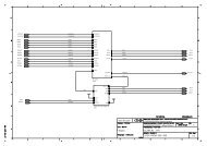
5.2 Logic Block Diagram CX65, M65<br />
TFT Display<br />
65k Farben<br />
132 x 176 pixels<br />
Display-Backlight<br />
(3 LEDs, white,<br />
integrated)<br />
Keyboard-<br />
Backlight<br />
(6 LEDs, white)<br />
Keyboard<br />
RF-<br />
Interface<br />
Joystic<br />
k<br />
5way<br />
Irda<br />
Clipit<br />
Pads<br />
B2B<br />
Night Design<br />
(2 LEDs, white)<br />
LIGHT_DISP<br />
LIGHT_KP<br />
KP_IN0<br />
KP_IN1<br />
KP_IN2<br />
KP_IN3<br />
KP_IN4<br />
KP_OUT0<br />
KP_OUT1<br />
KP_OUT2<br />
KB_ON_OFF<br />
Layout option<br />
only<br />
OR<br />
IR_AC_SEL<br />
IR_AC_RX<br />
IR_AC_TX<br />
LIGHT_PWM3<br />
SIM_IO<br />
SIM_RST<br />
SIM_CLK<br />
SIM<br />
SDRAM<br />
64 Mbit<br />
SGOLDlite<br />
PMB8875<br />
(ARM9/Teaklite)<br />
VDD_SIM<br />
Charge<br />
Control<br />
BATT+<br />
AKKU_TYP<br />
GND<br />
3<br />
LiIon-Akku 750mAh<br />
<strong>Service</strong> <strong>Repair</strong> <strong>Documentation</strong><br />
<strong>Level</strong> <strong>2.5e</strong> <strong>–</strong> <strong>HIT</strong> <strong>–</strong> C65, CX65 and M65<br />
3<br />
CS_SRAM / 1.8V /<br />
WR / RD<br />
POWER<br />
Ulysses<br />
CX65, M65<br />
A0...A24 / D0...D15<br />
Flash<br />
256 Mbit<br />
CS_FLASH / 1.8V<br />
/ WR / RD /<br />
PM_RESET_1.8V<br />
MIC1A<br />
GND_MIC<br />
SS<br />
C<br />
I2C<br />
Microphone<br />
Page 19 of 40<br />
32.768kHz<br />
I2C_DAT<br />
I2C_CLK<br />
IF Chip<br />
S1D 13716<br />
PM_SSC_MRST<br />
PM_SSC_MTSR<br />
PM_SSC_SCLK<br />
PMU: Mozart<br />
RX<br />
TX<br />
7<br />
2.9V<br />
1.5V_UC<br />
1.5V_DSP<br />
2.65V<br />
1.8V_MEM1<br />
1.8V_MEM2<br />
VDD_USB<br />
VDD_VIBRA<br />
VDD_SIM_CORE<br />
VDD_RTC<br />
VDD_PROX<br />
VDD_RF1<br />
VDD_RF2<br />
VGA<br />
Camera<br />
(480x640)<br />
USB_D+<br />
USB_D-<br />
2<br />
AC_RX<br />
AC_TX<br />
2<br />
AC_CTS<br />
AC_RTS<br />
AC_DCD<br />
5 GND_MIC<br />
MICEA<br />
POWER<br />
GND<br />
KB_ON_OFF<br />
ON/<br />
VDD_VIBRA<br />
Vibra<br />
USB<br />
I/O-Connector<br />
PROX_OUT1<br />
PROX_IN2<br />
2<br />
3<br />
STEREO1_OUT<br />
STEREO2_OUT<br />
PHANTOM_BUF_OUT<br />
MONO1_OUT 2<br />
MONO2_OUT<br />
Prox.-<br />
Sensor<br />
Speaker<br />
Release 1.0
Company Confi<strong>de</strong>ntial<br />
Copyright 2004© Siemens AG<br />
5.3 SGOLDLITE<br />
5.3.1 Digital Baseband<br />
Baseband Processor SGOLDlite (PMB8875)<br />
S-GOLDliteTM is a GSM single chip mixed signal baseband IC containing all analog and<br />
digital functionality of a cellular radio. The integrated circuit contains a ARM926EJ-S CPU<br />
and a TEAKLite DSP core. The ARM926EJ-S is a powerful standard controller and<br />
particularly suited for wireless systems. It is supported by a wi<strong>de</strong> range of tools and<br />
application SW. The TEAKLite is an established DSP core for wireless applications with<br />
approved firmware for GSM signal processing. The package is a P-LFBGA-345 (264<br />
functional pins + 81 thermical balls).<br />
Supported Standards<br />
• GSM speech FR, HR, EFR and AMR-NB<br />
• GSM data 2.4kbit/s, 4.8kbit/s, 9.6kbits, and 14.4kbit/s<br />
• HSCSD class 10<br />
• GPRS class 12<br />
Processing cores<br />
• ARM926EJ-S 32-bit processor core with operating frequency up to 125 MHz for<br />
controller functions<br />
• TEAKLite DSP core with operating frequency 104 MHz.<br />
ARM-Memory<br />
• 8 kByte Boot ROM on the AHB<br />
• 96 kByte SRAM on the AHB, flexibly usable as program or data RAM<br />
• 8 kByte Cache for Program (internal)<br />
• 8 kByte tightly coupled memory for Program (internal)<br />
• 8 kByte Cache for Data (internal)<br />
• 8 kByte tightly coupled memory for Data (internal)<br />
TEAKLite-Memory<br />
• 80 kwords Program ROM<br />
• 4 kwords Program RAM<br />
• 48 kwords Data ROM<br />
• 27 kwords Data RAM<br />
Shared Memory Blocks<br />
• 1.5 kwords Shared RAM (dual ported) between controller system and TEAKLite.<br />
<strong>Service</strong> <strong>Repair</strong> <strong>Documentation</strong><br />
<strong>Level</strong> <strong>2.5e</strong> <strong>–</strong> <strong>HIT</strong> <strong>–</strong> C65, CX65 and M65<br />
Page 20 of 40<br />
Release 1.0
Company Confi<strong>de</strong>ntial<br />
Copyright 2004© Siemens AG<br />
Functional Hardware blocks<br />
• CPU and DSP Timers<br />
• Programmable PLL with additional phase shifters for system clock generation<br />
• GSM Timer Module that off-loads the CPU from radio channel timing<br />
• GMSK Modulator according to GSM-standard 05.04 (5/2000)<br />
• Hardware accelerators for equalizer and channel <strong>de</strong>coding<br />
• Advanced static and dynamic power management features including TDMA-Frame<br />
synchronous low-power mo<strong>de</strong> and enhanced CPU mo<strong>de</strong>s (idle and sleep mo<strong>de</strong>s)<br />
Interfaces and Features<br />
• Keypad Interface for scanning keypads up to 6 rows and 4 columns<br />
• Pulse Number Modulation output for Automatic Frequency Correction (AFC)<br />
• Serial RF Control Interface; support of direct conversion RF<br />
• 2 USARTs with autobaud <strong>de</strong>tection and hardware flow control<br />
• IrDA Controller integrated in USART0 (with IrDA support up to 115.2 kbps)<br />
• 1 Serial Synchronous SPI compatible interfaces in the controller domain<br />
• 1 Serial Synchronous SPI compatible interface in the TEAKLite domain<br />
• I2C-bus interface (e.g. connection to S/M-Power)<br />
• 2 bidirectional and one unidirectional I2S interface accessible from the TEAKLite<br />
• USB V1.1 mini host interface for full speed <strong>de</strong>vices with up to 5 interfaces and 10<br />
endpoints configurable supporting also USB on-the-go functionality<br />
• ISO 7816 compatible SIM card interface<br />
• Enhanced digital (phase linearity, adj/ co-channel interference) baseband filters,<br />
including analog prefilters and high resolution analog-to-digital converters.<br />
• Separate analog-to-digital converter for various general purpose measurements like<br />
battery voltage, battery, VCXO and environmental temperature, battery technology,<br />
transmission power, offset, onchip temperature, etc.<br />
• Ringer support for highly oversampled PDM/PWM input signals for more versatility in<br />
ringer tone generation<br />
• RF power ramping functions<br />
• DAI Interface according to GSM 11.10 is implemented via <strong>de</strong>dicated I2S mo<strong>de</strong><br />
• 26 MHz master clock input<br />
• External memory interface:<br />
<strong>–</strong> 1.8V interface<br />
<strong>–</strong> Data bus: 16 bit non-multiplexed and multiplexed, 32 bit multiplexed<br />
<strong>–</strong> Supports synchronous <strong>de</strong>vices (SDRAMs and Flash Memory) up to 62.4 MHz<br />
<strong>–</strong> For each of the 4 address regions 128 MByte with 32-bit access or 64 MByte with<br />
a 16-bit access are addressable<br />
<strong>–</strong> Supports asynchronous <strong>de</strong>vices (i.e. SRAM, display) including write buffer for<br />
cache line write<br />
• Port logic for external port signals<br />
• Comprehensive static and dynamic Power Management<br />
<strong>–</strong> Various frequency options during operation mo<strong>de</strong><br />
<strong>–</strong> 32 kHz clock in standby mo<strong>de</strong><br />
<strong>–</strong> Sleep control in standby mo<strong>de</strong><br />
<strong>Service</strong> <strong>Repair</strong> <strong>Documentation</strong><br />
<strong>Level</strong> <strong>2.5e</strong> <strong>–</strong> <strong>HIT</strong> <strong>–</strong> C65, CX65 and M65<br />
Page 21 of 40<br />
Release 1.0
Company Confi<strong>de</strong>ntial<br />
Copyright 2004© Siemens AG<br />
<strong>–</strong> RAMs and ROMs in power save mo<strong>de</strong> during standby mo<strong>de</strong><br />
<strong>–</strong> Additional leakage current reduction in standby mo<strong>de</strong> possible by switching off<br />
the power for the TEAKLite subsystem.<br />
Baseband receive path<br />
In the receiver path the antenna input signal is converted to the base band, filtered, and<br />
amplified to target level by the RF transceiver chipset. The resulting differential I and Q<br />
baseband signals are fed into the S-GOLDliteTM. The A-to-D converter generates two 6.5<br />
Mbit/s data streams. The <strong>de</strong>cimation and narrowband channel filtering is done by a digital<br />
baseband filter for each path. The DSP performs for GMSK, the complex baseband signal<br />
equalization with soft-output recovery and the channel <strong>de</strong>coding supported by a Viterbi<br />
hardware accelerator. The recovered digital speech data is fed into the speech <strong>de</strong>co<strong>de</strong>r<br />
(D1300). The S-GOLDliteTM supports fullrate, halfrate, enhanced fullrate and adaptive<br />
multirate speech co<strong>de</strong>c algorithms.<br />
Baseband transmit path<br />
In the transmit direction the microphone signal is amplified and A-to-D converted by the<br />
D1300. The prefiltered and A-to-D converted voice signal passes a digital <strong>de</strong>cimation filter.<br />
Speech and channel encoding (including voice activity <strong>de</strong>tection, VAD, and discontinuous<br />
transmission, DTX) as well as digital GMSK modulation is carried out by the S-GOLDliteTM.<br />
The digital I and Q baseband components of the GMSK modulated signals (48-times<br />
oversampled with 13 MSamples/s) are D-to-A converted. The analog differential baseband<br />
signals are fed into the RF transceiver chipset. The RF transceiver modulates the baseband<br />
signal using a GMSK modulator. Finally, an RF power module amplifies the RF transmit<br />
signal to the required power level. The S-GOLDliteTM controller software controls the gain<br />
of the power amplifier by pre<strong>de</strong>fined ramping curves (16 words, 11 bit). The S-GOLDliteTM<br />
communicates with the RF chip set via a serial data interface.<br />
The following algorithms and a task scheduler are implemented on the DSP:<br />
Algorithms running on the DSP:<br />
• scanning of channels, i.e, measurement of the field strengths of neighbouring base<br />
stations<br />
• <strong>de</strong>tection and evaluation of Frequency Correction Bursts<br />
• equalisation of GMSK Normal Bursts and Synchronisation Bursts with bit-by-bit softoutput<br />
• Synch burst channel <strong>de</strong>co<strong>de</strong>r<br />
• channel encoding and soft-<strong>de</strong>cision <strong>de</strong>coding for fullrate, enhanced-fullrate and<br />
adaptive multirate speech, and control channels as well as RACH, PRACH<br />
• channel encoding for GPRS coding schemes (CS1-CS4) as well as USF <strong>de</strong>tection<br />
algorithms for the Medium Access Control (MAC) software layer<br />
• fullrate, enhanced fullrate and adaptive multirate speech encoding and <strong>de</strong>coding<br />
• support for fullrate (F9.6, F4.8, and F2.4) data channels<br />
<strong>Service</strong> <strong>Repair</strong> <strong>Documentation</strong><br />
<strong>Level</strong> <strong>2.5e</strong> <strong>–</strong> <strong>HIT</strong> <strong>–</strong> C65, CX65 and M65<br />
Page 22 of 40<br />
Release 1.0
Company Confi<strong>de</strong>ntial<br />
Copyright 2004© Siemens AG<br />
• mandatory sub-functions like<br />
<strong>–</strong> discontinuous transmission,<br />
<strong>–</strong> voice activity <strong>de</strong>tection, VAD<br />
<strong>–</strong> background noise calculation<br />
• generation of tone and si<strong>de</strong> tone<br />
• hands-free functions (acoustic echo cancellation, noise-reduction)<br />
• support for voice memo<br />
• support for voice dialling<br />
• handling of voco<strong>de</strong>r and voice-paths for type approval testing<br />
• ADPCM enco<strong>de</strong>r (8 kHz sampling frequency), cannot run in parallel to a speech<br />
co<strong>de</strong>c<br />
• ADPCM <strong>de</strong>co<strong>de</strong>r (8 kHz and 16 kHz sampling frequency), cannot run in parallel to a<br />
speech co<strong>de</strong>c<br />
Scheduler functions on the DSP:<br />
The scheduler is based on an operating system. It is basically triggered by interrupts<br />
generated by hardware peripherals or commands from the micro-controller.<br />
• communication between DSP and micro-controller<br />
• fully automatic handling of speech channels<br />
• semi-automatic handling of control channels<br />
• support of the GSM ciphering algorithm (A51, A52, A53) in combination with the<br />
hardware accelerator.<br />
• support for General Packet Radio <strong>Service</strong>s (GPRS) with up to 4 Rx and 1Tx or 3 Rx<br />
and 2 Tx (Class 10 mobile).<br />
• monitoring of paging blocks for packet switched and circuit switched services<br />
simultaneously GPRS MS in Class-B mo<strong>de</strong> of operation<br />
• MMS support<br />
• loop-back functions (according to GSM 11.10)<br />
Real Time Clock<br />
The real time clock (<strong>de</strong>gree of accuracy 150ppm) is powered via a separate voltage<br />
regulator insi<strong>de</strong> the ASIC. Via a capacitor, data is kept in the internal RAM during a battery<br />
change for at least 30 seconds. An alarm function is also integrated with which it is possible<br />
to switch the phone on and off.<br />
Measurement of Battery voltage, Battery Type and Ambient Temperature<br />
The voltage equivalent of the temperature and battery co<strong>de</strong> on the voltage separator will be<br />
calculated as the difference against a reference voltage of the S-GOLDlite. Insi<strong>de</strong> the S-<br />
GOLDlite are some analog to digital converters. These are used to measure the battery<br />
voltage, battery co<strong>de</strong> resistor and the ambient temperature.<br />
Timing of the Battery Voltage Measurement<br />
Unless the battery is being charged, the measurement shall be ma<strong>de</strong> in the TX time slot. During<br />
charging it will be done after the TX time slot.<br />
<strong>Service</strong> <strong>Repair</strong> <strong>Documentation</strong><br />
<strong>Level</strong> <strong>2.5e</strong> <strong>–</strong> <strong>HIT</strong> <strong>–</strong> C65, CX65 and M65<br />
Page 23 of 40<br />
Release 1.0
Company Confi<strong>de</strong>ntial<br />
Copyright 2004© Siemens AG<br />
5.3.2 SDRAM<br />
Memory for volatile data. SDRAM= synchronous High data rate Dynamic RAM<br />
Memory Size: 64 Mbit<br />
Data Bus: 16 Bit<br />
Frequency: 105 MHz<br />
Power supply: 1.8 V<br />
5.3.3 FLASH<br />
Non-volatile but <strong>de</strong>letable and re-programmable (software update) program memory for the<br />
S-GOLDlite and for saving e.g. user data (menu settings), voice band data (voice memo),<br />
mobile phone matching data, images etc.. There is a serial number on the flash which<br />
cannot be changed.<br />
Memory Size 256 Mbit (32 MByte)<br />
Data Bus: 16 Bit<br />
Access Time: Initial access: 85 ns<br />
Synchronous Burst Mo<strong>de</strong>: 54 MHz / 14ns clock to data output<br />
Asynchronous Mo<strong>de</strong>: 85 ns<br />
5.3.4 SIM<br />
SIM cards with supply voltages of 1.8V and 3V are supported. 1.8V cards are supplied with<br />
3V.<br />
5.3.5 Vibration Motor<br />
The vibration motor is mounted in the lower case. The electrical connection to the PCB is<br />
realised with pressure contacts.<br />
fom ASIC D1300<br />
<strong>Service</strong> <strong>Repair</strong> <strong>Documentation</strong><br />
<strong>Level</strong> <strong>2.5e</strong> <strong>–</strong> <strong>HIT</strong> <strong>–</strong> C65, CX65 and M65<br />
Page 24 of 40<br />
Release 1.0
Company Confi<strong>de</strong>ntial<br />
Copyright 2004© Siemens AG<br />
6 Power Supply<br />
6.1 ASIC Mozart / Twigo4<br />
The power supply ASIC will contain the following functions:<br />
• Powerdown-Mo<strong>de</strong><br />
• Sleep Mo<strong>de</strong><br />
• Trickle Charge Mo<strong>de</strong><br />
• Power on Reset<br />
• Digital state machine to control switch on and supervise the uC with a<br />
watchdog<br />
• 17 Voltage regulators<br />
• 2 internal DC/DC converters (Step-up and Step-down converter)<br />
• Low power voltage regulator<br />
• Additional output ports<br />
• Voltage supervision<br />
• Temperature supervision with external and internal sensor<br />
• Battery charge control<br />
• TWI Interface (I 2 C interface)<br />
• Bandgap reference<br />
• High performance audio quality<br />
• Audio multiplexer for selection of audio input<br />
• Audio amplifier stereo/mono<br />
• 16 bit Sigma/Delta DAC with Clock recovery and I 2 S Interface<br />
6.1.1 Battery<br />
As a standard battery a LiIon battery with a nominal capacity of 780mAh@0.2CA* and GSM<br />
capacity** of min. 750mAh will be provi<strong>de</strong>d.<br />
* battery will be discharged with 20% of capacity rate till 2.75V; e.g. R65, 0.2x750mA=150mA<br />
** battery will be discharged with 2A(0.6ms)+0.25A(0.4ms) till 3.2V.<br />
6.1.2 Charging Concept<br />
6.1.2.1 General<br />
The battery is charged in the phone. The hardware and software is <strong>de</strong>signed for LiIon with<br />
4.2V technology. Charging is started as soon as the phone is connected to an external<br />
charger. If the phone is not switched on, then charging shall take place in the background<br />
(the customer can see this via the “Charge” symbol in the display). During normal use the<br />
phone is being charged (restrictions: see below). Charging is enabled via a PMOS switch in<br />
the phone. This PMOS switch closes the circuit for the external charger to the battery. The<br />
processor takes over the control of this switch <strong>de</strong>pending on the charge level of the battery,<br />
whereby a disable function in the ASIC hardware can overri<strong>de</strong>/interrupt the charging in the<br />
case of over voltage of the battery<br />
<strong>Service</strong> <strong>Repair</strong> <strong>Documentation</strong><br />
<strong>Level</strong> <strong>2.5e</strong> <strong>–</strong> <strong>HIT</strong> <strong>–</strong> C65, CX65 and M65<br />
Page 25 of 40<br />
Release 1.0
Company Confi<strong>de</strong>ntial<br />
Copyright 2004© Siemens AG<br />
For controlling the charging process it is necessary to measure the ambient (phone)<br />
temperature and the battery voltage. The temperature sensor will be an NTC resistor with a<br />
nominal resistance of 22kΩ at 25°C. The <strong>de</strong>termination of the temperature is achieved via a<br />
voltage measurement on a voltage divi<strong>de</strong>r in which one component is the NTC. Charging is<br />
ongoing as long the temperature is within the range +5°C to 45°C. The maximal charge time<br />
will be 2 hours (Imax=750mA).<br />
6.1.2.2 Measurement of Battery voltage, Battery Type and Ambient Temperature<br />
The voltage equivalent of the temperature and battery co<strong>de</strong> on the voltage separator will be<br />
calculated as the difference against a reference voltage of the S-GOLDlite. Insi<strong>de</strong> the S-<br />
GOLDlite are some analog to digital converters. These are used to measure the battery<br />
voltage, battery co<strong>de</strong> resistor and the ambient temperature.<br />
6.1.2.3 Timing of the Battery Voltage Measurement<br />
Unless the battery is being charged, the measurement shall be ma<strong>de</strong> in the TX time slot.<br />
During charging it will be done after the TX time slot.<br />
6.1.2.4 Recognition of the Battery Type<br />
The different batteries will be enco<strong>de</strong>d by different resistors within the battery pack itself.<br />
6.1.2.5 Charging Characteristic of Lithium-Ion Cells<br />
LiIon batteries are charged with a U/I characteristic, i.e. the charging current is regulated in<br />
relation to the battery voltage until a minimal charging current has been achieved. The<br />
maximum charging current is given by the connected charger. The battery voltage may not<br />
exceed 4.2V ±50mV average. During the charging pulse current the voltage may reach<br />
4.3V. The temperature range in which charging of the phone may be performed is in the<br />
ranges from 0...50°C. Outsi<strong>de</strong> this range no charging takes place, the battery only supplies<br />
current.<br />
6.1.2.6 Trickle Charging<br />
The ASIC is able to charge the battery at voltages below 3.2V without any support from the<br />
charge SW. The current will by measured indirectly via the voltage drop over a shunt<br />
resistor and linearly regulated insi<strong>de</strong> the ASIC by means of the external FET. The current<br />
level during trickle charge for voltages
M<br />
Company Confi<strong>de</strong>ntial<br />
Copyright 2004© Siemens AG<br />
6.1.2.8 USB Charging<br />
The ASIC can support USB charging when USB charging is integrated in the charging<br />
software. If charge voltage is in the range 4.4V to 5.25 V USB charging is ongoing. During<br />
USB charging only limited charging is possible. Charge current is limited to 75, 150, 300 or<br />
400 mA.<br />
6.1.2.9 Audio multiplexer<br />
I/O-Connector<br />
I/O-Connector<br />
Mono Headset<br />
HP<br />
SPK<br />
MONO1_OUT<br />
MONO2_OUT<br />
MONO1_IN<br />
MONO2_IN<br />
MONO1_LP_OUT<br />
MONO2_LP_OUT<br />
STEREO1_OUT<br />
PHANTOM_BUFF_OUT<br />
HP<br />
MICBIAS<br />
HP<br />
MIC<br />
HP<br />
MICE<br />
STEREO1_OUT<br />
Vibra<br />
MICBIAS<br />
MIC1<br />
MIC2<br />
MICE1<br />
MICE2<br />
PWM<br />
Mozart / Twigo 4<br />
KEY-CLICK<br />
&Ringing<br />
<strong>Service</strong> <strong>Repair</strong> <strong>Documentation</strong><br />
<strong>Level</strong> <strong>2.5e</strong> <strong>–</strong> <strong>HIT</strong> <strong>–</strong> C65, CX65 and M65<br />
MUX<br />
MUX<br />
...<br />
DAC<br />
DAC<br />
DIV<br />
DIV<br />
ADC<br />
ADC<br />
Control<br />
PLL<br />
I²S<br />
I²S<br />
RINGIN<br />
I²C / TWI<br />
SSC<br />
I²S<br />
LINE1<br />
LINE2<br />
26MHz<br />
I²S<br />
BB & RF<br />
Bluetooth<br />
I²S_1<br />
I²S_2<br />
RINGIN<br />
I²C / TWI<br />
I²S_1<br />
Page 27 of 40<br />
SSC<br />
I²S_2<br />
EP1<br />
EP2<br />
MIC1<br />
MIC2<br />
VMIC<br />
SGold lite<br />
MUX<br />
LP Filter<br />
MCU<br />
NB<br />
DAC<br />
NB<br />
ADC<br />
Voice<br />
Recording<br />
DSP<br />
Deco<strong>de</strong>r<br />
BB<br />
GSM<br />
Enco<strong>de</strong>r<br />
Release 1.0<br />
RF<br />
GSM
Company Confi<strong>de</strong>ntial<br />
Copyright 2004© Siemens AG<br />
7 Camera<br />
The camera module uses a colour sensor with a full VGA (640x480) resolution in landscape<br />
orientation. The module will <strong>de</strong>liver an 8Bit output signal which will be pre-processed by the<br />
EPSON S1D13716 graphic engine chip. Various settings like brightness, image<br />
stabilization, white balance can be done by using the I2C interface.<br />
Camera Board-to-Board Connector<br />
8 Camera <strong>–</strong> Display Interface Module<br />
For the interface between S-GOLDlite, camera and display a graphics engine chip called<br />
S1D13716 from Epson is used. By using the SSC interface the S-GOLDlite communicates<br />
with this graphic engine chip. The S1D13716 has a second SSC interface to adapt the<br />
display. Over an I2C interface, provi<strong>de</strong>d by the S1D13716, the camera-module can be<br />
initialised; the picture-data output of the camera goes over a parallel 8-bit interface<br />
There are three mo<strong>de</strong>s available:<br />
a) Bypass mo<strong>de</strong>:<br />
In this mo<strong>de</strong> the S1D13716 is transparent regarding the display. The S-GOLDlite<br />
communicates “directly” with the display.<br />
b) Camera View Mo<strong>de</strong>:<br />
In this mo<strong>de</strong> the S1D13716 transfers the picture <strong>–</strong> data from the camera directly<br />
to the display. A resizing and compressing engine is available to reduce the data<br />
amount to the display. So the preview can be done without using the SGOD<br />
performance.<br />
Page 28 of 40<br />
<strong>Service</strong> <strong>Repair</strong> <strong>Documentation</strong><br />
<strong>Level</strong> <strong>2.5e</strong> <strong>–</strong> <strong>HIT</strong> <strong>–</strong> C65, CX65 and M65<br />
To EPSON S1D13716<br />
Release 1.0
Company Confi<strong>de</strong>ntial<br />
Copyright 2004© Siemens AG<br />
c) Camera Capture Mo<strong>de</strong>:<br />
In this mo<strong>de</strong> the picture <strong>–</strong> data from the camera is sent to the SGOLD. There are resizing<br />
and compressing engines available to reduce the data-stream to the SGOLD-lite<br />
Camera Interface<br />
Display Interface<br />
Voltage supply for Camera Asic<br />
<strong>Service</strong> <strong>Repair</strong> <strong>Documentation</strong><br />
<strong>Level</strong> <strong>2.5e</strong> <strong>–</strong> <strong>HIT</strong> <strong>–</strong> C65, CX65 and M65<br />
Page 29 of 40<br />
SSC + control lines to<br />
SGOLD lite<br />
Release 1.0
Company Confi<strong>de</strong>ntial<br />
Copyright 2004© Siemens AG<br />
9 Display Modules<br />
9.1 Display C65<br />
The C65 display has a resolution of 130x130 pixels with a colour <strong>de</strong>pth of 65536 colours. It<br />
contains an passive matrix panel (CSTN ) where the colours are generated by red, green<br />
and blue colour filters and a plastic housing. For the display two different sources are used ,<br />
which will be distinguished by the software via different co<strong>de</strong> resistor values. Both modules<br />
use different LCD-controllers. The controller is directly mounted on the panel of the display<br />
(COG). In or<strong>de</strong>r to guarantee a very efficient illumination the white LEDs are mounted on a<br />
flexfoil insi<strong>de</strong> the module. In addition, all passive components necessary to drive an LCD<br />
are also assembled on this flexfoil. The software can <strong>de</strong>tect the displays automatically due<br />
to the hardware coding. Thus, the only interconnections to the Siemens PCB are the data<br />
lines and the power supply lines of the controller and the white LEDs. The interface is<br />
realized by spring connector with 10 interconnections which is assembled on the Siemens<br />
PCB.<br />
9.2 Display CX65, M65<br />
The CX65, M65 display has a resolution of 132x176 pixels with a color <strong>de</strong>pth of 65536<br />
colors. It contains an active-matrix panel where the colors are generated by red, green and<br />
blue color filters and a plastic housing. For the display two different sources are used, which<br />
will be distinguished by the software via different co<strong>de</strong> resistor values. Both modules use<br />
different LCD-controllers. The controller is directly mounted on the panel of the display. In<br />
or<strong>de</strong>r to guarantee a very efficient illumination the white LEDs are mounted on a flexfoil<br />
insi<strong>de</strong> the module. In addition, all passive components necessary to drive an LCD are also<br />
assembled on this flexfoil. The software can <strong>de</strong>tect the displays automatically due to the<br />
hardware coding. Thus, the only interconnections to the Siemens PCB are the data lines<br />
and the power supply lines of the controller and the white LEDs. The interface is realized by<br />
spring connector with 10 interconnections which is assembled on the Siemens PCB.<br />
<strong>Service</strong> <strong>Repair</strong> <strong>Documentation</strong><br />
<strong>Level</strong> <strong>2.5e</strong> <strong>–</strong> <strong>HIT</strong> <strong>–</strong> C65, CX65 and M65<br />
Page 30 of 40<br />
Release 1.0
Company Confi<strong>de</strong>ntial<br />
Copyright 2004© Siemens AG<br />
The display controller is being driven with a supply voltage of VDD1_2.9V = 2.90 V and<br />
VDD2_1.8V=1.8 V. The 3 white si<strong>de</strong>-shooter LEDs are driven in serial. The maximum<br />
current is 15mA. The voltage for the 3 LEDs is VDD_Boost.<br />
<strong>Service</strong> <strong>Repair</strong> <strong>Documentation</strong><br />
<strong>Level</strong> <strong>2.5e</strong> <strong>–</strong> <strong>HIT</strong> <strong>–</strong> C65, CX65 and M65<br />
Page 31 of 40<br />
Release 1.0
Company Confi<strong>de</strong>ntial<br />
Copyright 2004© Siemens AG<br />
10 Illumination<br />
a) Keyboard<br />
The LED´s will be mounted on separate MMI-PCB. The illumination of the keypad will be<br />
done via high-brightness LEDs (colour: white, type: top-shooter, driven by 7.5 mA / LED).<br />
The LEDs will be driven by one current source with a maximum current of 15 mA. The 6<br />
LEDs are divi<strong>de</strong>d in two groups with 3 LEDs in serial.<br />
b) Display<br />
The 3 serial LEDs for the display are supplied by one constant current sources, to ensure<br />
the same brigthness and colour of the white backlight.<br />
<strong>Service</strong> <strong>Repair</strong> <strong>Documentation</strong><br />
<strong>Level</strong> <strong>2.5e</strong> <strong>–</strong> <strong>HIT</strong> <strong>–</strong> C65, CX65 and M65<br />
Page 32 of 40<br />
Release 1.0
Company Confi<strong>de</strong>ntial<br />
Copyright 2004© Siemens AG<br />
c) Dynamic Light only CX65 and M65<br />
The 2 white LEDs for the dynamic light are directly contacted to the battery pack. One<br />
transistor is used for both LEDs to control the brightness. Also a PWM is necessary to<br />
prevent a damage of the LEDs when the battery pack is fully charged.<br />
<strong>Service</strong> <strong>Repair</strong> <strong>Documentation</strong><br />
<strong>Level</strong> <strong>2.5e</strong> <strong>–</strong> <strong>HIT</strong> <strong>–</strong> C65, CX65 and M65<br />
Page 33 of 40<br />
Release 1.0
Company Confi<strong>de</strong>ntial<br />
Copyright 2004© Siemens AG<br />
11 Interfaces<br />
11.1 Microphone<br />
Pin Name IN/OUT Remarks<br />
1 MIC1A O Microphone power supply. The same line carries the low<br />
frequency speech signal.<br />
2 MIC1B GND_MIC<br />
11.2 Loudspeaker<br />
Pin Name IN/OU<br />
T<br />
Remarks<br />
1 MONO1_OUT O 1st connection to the internal earpiece. Earpiece can be<br />
switched off in the case of accessory operation. EPP1 builds<br />
together with EPN1 the differential output to drive the<br />
multifunctional “earpiece” (earpiece, ringer, handsfree<br />
function).<br />
2 MONO2_OUT O 2nd connection to the internal earpiece. Earpiece can be<br />
switched off in the case of accessory operation.<br />
<strong>Service</strong> <strong>Repair</strong> <strong>Documentation</strong><br />
<strong>Level</strong> <strong>2.5e</strong> <strong>–</strong> <strong>HIT</strong> <strong>–</strong> C65, CX65 and M65<br />
Page 34 of 40<br />
Release 1.0
Company Confi<strong>de</strong>ntial<br />
Copyright 2004© Siemens AG<br />
11.3 Battery<br />
<strong>Service</strong> <strong>Repair</strong> <strong>Documentation</strong><br />
<strong>Level</strong> <strong>2.5e</strong> <strong>–</strong> <strong>HIT</strong> <strong>–</strong> C65, CX65 and M65<br />
Pin Name <strong>Level</strong> Remarks<br />
1 GND - Ground<br />
2 AKKU_TYP 0V...2.65V Recognition of<br />
battery/supplier<br />
3 BATT+ 3 V... 4.5V Positive battery pole<br />
11.4 IRDA<br />
A Low-Power infrared data interface, compatible to ”IrDA - Infrared Data Association; Serial<br />
Infrared Physical Layer Specification, Version 1.3”, supporting transmission rates up to<br />
115.2kbps (Slow IrDA) will be provi<strong>de</strong>d. As a Low-Power-Device, the infrared data interface<br />
has a transmission range of at least:<br />
• 20cm to other Low-Power-Devices and<br />
• 30cm to Standard-Devices<br />
Page 35 of 40<br />
Release 1.0
Company Confi<strong>de</strong>ntial<br />
Copyright 2004© Siemens AG<br />
11.5 Interface SIM Module<br />
Pin Name IN/OUT Remarks<br />
SIM_CLK O Pulse for chipcard.<br />
The chipcard is controlled directly from the SGOLD+.<br />
SIM_RST O Reset for chipcard<br />
SIM_IO I<br />
Data pin for chipcard;<br />
O<br />
4,7 kΩ pull up at the VDD_SIM pin<br />
VDD_SIM O Switchable power supply for chipcard;<br />
220 nF capacitors are situated close to the chipcard pins<br />
and are necessary for buffering current spikes.<br />
<strong>Service</strong> <strong>Repair</strong> <strong>Documentation</strong><br />
<strong>Level</strong> <strong>2.5e</strong> <strong>–</strong> <strong>HIT</strong> <strong>–</strong> C65, CX65 and M65<br />
Page 36 of 40<br />
Release 1.0
Company Confi<strong>de</strong>ntial<br />
Copyright 2004© Siemens AG<br />
11.6 IO Connector with ESD protection<br />
11.6.1 IO Connector <strong>–</strong> New Slim Lumberg<br />
Pin Name IN/OUT Notes<br />
1 POWER I/O POWER is nee<strong>de</strong>d for charging batteries and for supplying the<br />
accessories. If accessories are supplied by mobile, talk-time<br />
and standby-time from telephone are reduced. Therefore it has<br />
to be respected on an as low as possible power consumption in<br />
the accessories.<br />
2 GND<br />
3 TX/D+ OI/O Serial interface<br />
USB-interface full-speed 12Mbit/s<br />
4 RX/D-<br />
I Serial interface<br />
USB-interface<br />
full-speed 12Mbit/s<br />
5 DATA/CTS I/O Data-line for accessory-bus<br />
Use as CTS in data operation.<br />
6 RTS I/O Use as RTS in data-operation.<br />
7 CLK/DCD I/O Clock-line for accessory-bus.<br />
Use as DTC in data-operation.<br />
8 STEREO1_OUT Analog O driving ext. headset STEREO1_OUT and STEREO2_OUT<br />
differential mo<strong>de</strong><br />
9 GND<br />
10 STEREO2_OUT Analog O driving ext. right to PHANTOM_BUF_OUT with mono-headset<br />
STEREO1_OUT and STEREO2_OUT differential mo<strong>de</strong><br />
11 GND_MIC Analog I for ext. microphone<br />
12 MICEA_AC Analog I External microphone<br />
<strong>Service</strong> <strong>Repair</strong> <strong>Documentation</strong><br />
<strong>Level</strong> <strong>2.5e</strong> <strong>–</strong> <strong>HIT</strong> <strong>–</strong> C65, CX65 and M65<br />
Page 37 of 40<br />
Release 1.0
Company Confi<strong>de</strong>ntial<br />
Copyright 2004© Siemens AG<br />
11.6.2 ESD Protection with EMI filter<br />
The Z1500 is a 5-channel filter with over-voltage and ESD Protection array which is<br />
<strong>de</strong>signed to provi<strong>de</strong> filtering of un<strong>de</strong>sired RF signals in the 800-4000MHz frequency band<br />
Additionally the Z1500 contains dio<strong>de</strong>s to protect downstream components from<br />
Electrostatic Discharge (ESD) voltages<br />
<strong>Service</strong> <strong>Repair</strong> <strong>Documentation</strong><br />
<strong>Level</strong> <strong>2.5e</strong> <strong>–</strong> <strong>HIT</strong> <strong>–</strong> C65, CX65 and M65<br />
Page 38 of 40<br />
Release 1.0
Company Confi<strong>de</strong>ntial<br />
Copyright 2004© Siemens AG<br />
11.7 Vibration Motor<br />
The vibration motor is mounted in the lower case. The electrical connection to the PCB is realised<br />
with pressure contacts<br />
Pin Name IN/OU<br />
T<br />
Remarks<br />
1 VDD_VIBRA Vbatt will be switched by PWM-signal with<br />
internal FET to VDD_Vibra in Asic<br />
2 GND<br />
<strong>Service</strong> <strong>Repair</strong> <strong>Documentation</strong><br />
<strong>Level</strong> <strong>2.5e</strong> <strong>–</strong> <strong>HIT</strong> <strong>–</strong> C65, CX65 and M65<br />
Page 39 of 40<br />
Release 1.0
Company Confi<strong>de</strong>ntial<br />
Copyright 2004© Siemens AG<br />
12 Keyboard<br />
The keyboard is connected via the lines KPOUT0 <strong>–</strong> KPOUT3 and KPIN0 <strong>–</strong> KPIN4 with the<br />
SGOLDLITE. KB_ON_OFF is used for the ON/OFF switch. KP_INO is used for the si<strong>de</strong><br />
keys. KPIN0 <strong>–</strong> KPIN4 and KPOUT3 is used for the joystick.<br />
<strong>Service</strong> <strong>Repair</strong> <strong>Documentation</strong><br />
<strong>Level</strong> <strong>2.5e</strong> <strong>–</strong> <strong>HIT</strong> <strong>–</strong> C65, CX65 and M65<br />
Page 40 of 40<br />
Release 1.0