The IC Package
The IC Package
The IC Package

You also want an ePaper? Increase the reach of your titles
YUMPU automatically turns print PDFs into web optimized ePapers that Google loves.
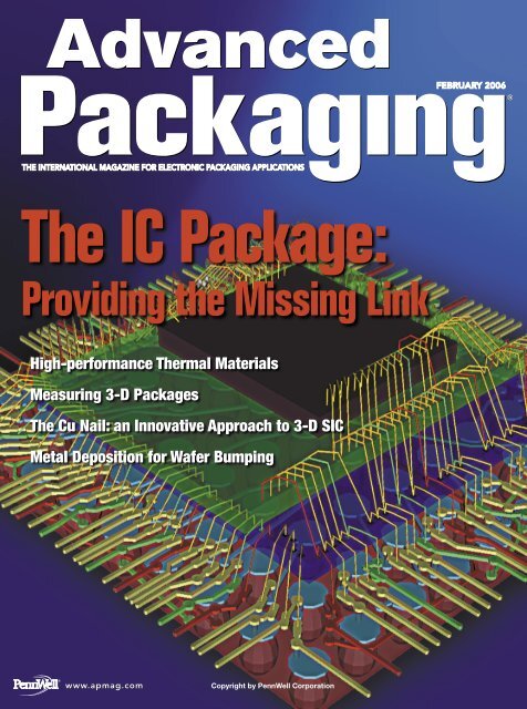
FEBRUARY 2006<br />
THE INTERNATIONAL MAGAZINE FOR ELECTRON<strong>IC</strong> PACKAGING APPL<strong>IC</strong>ATIONS<br />
<strong>The</strong> <strong>IC</strong> <strong>Package</strong>:<br />
Providing the Missing Link<br />
High-performance <strong>The</strong>rmal Materials<br />
Measuring 3-D <strong>Package</strong>s<br />
<strong>The</strong> Cu Nail: an Innovative Approach to 3-D S<strong>IC</strong><br />
Metal Deposition for Wafer Bumping<br />
www.apmag.com<br />
Copyright by PennWell Corporation
<strong>The</strong> <strong>IC</strong> <strong>Package</strong><br />
Cover Image<br />
courtesy of<br />
Cadence Design Systems<br />
MISSING LINK BETWEEN NANOMETER SIL<strong>IC</strong>ON AND MULTI-GIGABIT PCB SYSTEMS<br />
BY AN-YU KUO AND ZHEN MU<br />
As nanometer-scale <strong>IC</strong>s become<br />
commonplace andprinted<br />
circuit board (PCB)<br />
system data rates achieve<br />
multi-gigabit levels, it is increasingly<br />
important for designers to consider the<br />
entire system interconnect — from <strong>IC</strong><br />
to package to board to package. From<br />
this vantage point, <strong>IC</strong> package design<br />
takes on new importance. It becomes<br />
the critical link in the signal and power<br />
paths where money and time are<br />
gained or lost.<br />
In the face of this pressure, highspeed<br />
<strong>IC</strong> package designers must ensure<br />
both signal and power integrity<br />
by making certain <strong>IC</strong> package structures<br />
are properly modeled, extracted,<br />
and simulated with the rest of the circuit<br />
on both signal and power delivery<br />
paths. Fortunately, integrated modeling<br />
and analysis techniques and tools<br />
are available to describe a complicated<br />
package structure with true 3-D representations,<br />
and simulate those representations<br />
in the context of system<br />
interconnect. <strong>The</strong>se tools help designers<br />
consider the package effect from<br />
designs and make decisions based on<br />
actual conditions, thus reducing design<br />
iterations, cycles, and development<br />
time.<br />
3-D Modeling<br />
As modeling is an integral part of the<br />
design and analysis of <strong>IC</strong> packages, it<br />
is important to look at the options. For<br />
the past two decades, 2-D field solvers<br />
have been used successfully for<br />
modeling traces on PCBs. However,<br />
increasing package complexity and<br />
density has resulted in signal traces<br />
with more vias, segments, and discontinuities.<br />
Complex packages place<br />
traces on many layers. <strong>Package</strong>-interconnect<br />
elements, such as nonorthogonal<br />
traces, vias, wire bonds, and solder<br />
balls must be modeled. As 2-D field<br />
solvers cannot address 3-D behaviors,<br />
3-D solutions have to be used. <strong>The</strong>re<br />
are two types of complementary 3-D<br />
field solvers — full-wave and quasistatic<br />
— that are useful in representing<br />
package behavior, depending on<br />
the application. Both can be used in<br />
conjunction with 2-D solvers.<br />
As illustrated in Figure 1, signals<br />
propagate in a simple transverse electromagnetic<br />
(TEM) mode on long<br />
transmission lines. For these designs,<br />
traditional 2-D field solvers are<br />
accurate enough and much faster than<br />
3-D field solvers. However, Figure 2<br />
shows how signal propagation modes<br />
in packages require a 3-D field solver.<br />
Quasi-static and Full-wave<br />
Field Solvers<br />
Quasi-static field solvers are used when<br />
signals traveling on conductive paths<br />
have lower speeds — usually data<br />
rates below 5 Gbps. Quasi-static solvers<br />
produce field solutions by ignoring<br />
the displacement current. With such<br />
simplification, electrical fields remain<br />
static outside conductors, but magnetic<br />
fields retain frequency dependency<br />
inside conductors so that the skin effect<br />
can be accounted for properly.<br />
Capacitance (C) and conductance (G)<br />
of a structure are determined by electrical<br />
fields only; resistance (R) and<br />
Photo courtesy of Amkor Technologies, Inc.
89591.5<br />
83992.0<br />
78392.6<br />
72793.1<br />
67193.6<br />
61594.2<br />
55994.7<br />
50395.2<br />
44795.8<br />
39196.3<br />
33596.8<br />
27997.3<br />
22397.9<br />
16798.4<br />
11198.9<br />
5599.5<br />
0<br />
Figure 1. Electrical field distribution on a long differential pair.<br />
inductance (L) are determined only by<br />
magnetic 0602apKuof1 fields. In other words, by ignoring<br />
the displacement current, magnetic<br />
and electrical<br />
147849.0<br />
fields are decoupled<br />
138608.4<br />
in the quasi-static<br />
129367.9<br />
theory, and can be<br />
120127.3<br />
solved independently.<br />
Because of the<br />
110886.8<br />
101646.2<br />
92405.6<br />
decoupling between<br />
83165.1<br />
electrical and magnetic<br />
fields, a qua-<br />
64683.9<br />
73924.5<br />
si-static field solver 55443.4<br />
46202.8<br />
is quicker and can<br />
36962.3<br />
solve much bigger<br />
27721.7<br />
problems than a fullwave<br />
solver. Many 9240.6<br />
18481.1<br />
0<br />
modern quasi-static<br />
solvers can perform<br />
whole-package<br />
RLGC extraction of a complicated<br />
package design in a few hours.<br />
0602apKuof2<br />
Most designers wonder about the<br />
highest frequency at which the quasistatic<br />
assumption is still valid. While it<br />
is difficult to provide a universal upper<br />
limit to the applicability of quasi-static<br />
solvers, in high-speed package designs, 3<br />
to 4 GHz is an acceptable value.<br />
Full-wave field solvers are used in cases<br />
where strong electromagnetic coupling,<br />
resonance, and radiation require<br />
accurate solutions of Maxwell equations.<br />
A full-wave field solver is capable<br />
of solving Maxwell equations at any<br />
given frequency. It solves electrical and<br />
magnetic fields together so that the interaction<br />
between electrical and magnetic<br />
fields is handled properly. As a result,<br />
this type of solver can take into account<br />
displacement currents,<br />
electromagnetic<br />
radiation, and<br />
field coupling. Because<br />
there are limits<br />
in computer capacities,<br />
full-wave field<br />
solvers are best applied<br />
to obtain solutions<br />
of small geometries;<br />
for example,<br />
z coupled critical signal<br />
traces carrying<br />
y<br />
x 12.5-Gbps signals.<br />
In practice, designers<br />
will use 3-D field<br />
solvers in addition to<br />
2-D solvers. While the choice of field solvers<br />
is application-dependent, any field<br />
solver must be integrated into a design<br />
Figure 2. Electrical field distribution of a package model.<br />
Integrating Packaging Effects 0602apKuof3 in<br />
z<br />
I/O<br />
driver<br />
system that enables engineers<br />
to explore, design,<br />
implement, and<br />
verify interconnect topologies<br />
and electrical<br />
constraints through<br />
simulation. Such an integrated<br />
environment<br />
can eliminate time<br />
wasted in translations<br />
and re-entering of design<br />
data, in addition to ensuring product<br />
performance.<br />
x<br />
y<br />
RC model<br />
of RDL<br />
Represent<br />
RDL from <strong>IC</strong> tool<br />
High-Speed Design<br />
Today’s high-speed digital systems are<br />
characterized by high current capacity,<br />
high data rates, and low voltage,<br />
forcing design focus on power delivery.<br />
<strong>The</strong> challenge of providing sufficient<br />
and stable power to active devices<br />
through PCBs and packages<br />
elevates power delivery design to the<br />
system level. To solve the problem,<br />
the <strong>IC</strong>, package, and board must be<br />
considered.<br />
To illustrate how designers can use 3-<br />
D package representations and efficiently<br />
simulate those representations within a<br />
cross-domain environment, an example<br />
demonstrates addressing signal delays by<br />
modeling package interconnects with a<br />
quasi-static 3-D field solver, and by simulating<br />
the entire signal paths from output<br />
buffers to input buffers. This differs<br />
from the typical current flow/methodology<br />
where the power supply to the <strong>IC</strong><br />
core is assumed ideal, or at best, attenuated<br />
by a lumped, fixed-impedance, approximated<br />
load meant to represent the<br />
<strong>IC</strong> package and the PCB.<br />
Figure 3 shows the die-to-die signal path<br />
and highlights the importance of working<br />
in an integrated design and analysis environment<br />
that allows for cross-domain<br />
communication. It is a virtual or abstract<br />
system interconnect model (VS<strong>IC</strong>), which<br />
enables complete modeling and analysis<br />
of the interconnect across silicon, package,<br />
and PCB. <strong>The</strong> redistribution layer<br />
(RDL) model is drawn from the <strong>IC</strong> database,<br />
the package parasitics from the <strong>IC</strong><br />
package tool, and the board trace models<br />
from the PCB layout tool.<br />
Figure 4 provides a look at the simulation<br />
flow for the same circuit within<br />
3-D model extraction<br />
for package parasitics<br />
<strong>Package</strong><br />
parasitics<br />
RDL and package<br />
repeating here<br />
(ignored)<br />
I/O<br />
receiver<br />
Trace model<br />
on board<br />
2-D model of<br />
traces on board<br />
Figure 3. VS<strong>IC</strong> model of a buffer-to-buffer interconnect pathway.<br />
the design and analysis environment.<br />
Following the simulation flow, a net<br />
on the design can be modeled in three<br />
pieces: the RDL equivalent model, the<br />
3-D package model, and the 2-D board<br />
trace model. By simulating the extracted<br />
circuit, signal distortion and delay<br />
between output buffer and input buffer<br />
can be measured.
C O V E R S T O R Y<br />
Driver I/O:<br />
model<br />
Receiver I/O:<br />
model<br />
Integrated design and analysis environment<br />
<strong>Package</strong> layout file<br />
3-D package<br />
model extraction<br />
(RLGC, S-parameter)<br />
Simulating signal path<br />
(single or coupled)<br />
Measure and report<br />
signal degradation,<br />
crosstalk, and delays<br />
from die pad to board<br />
through package<br />
To ensure power integrity, two fundamental<br />
design requirements must be<br />
0602apKuof4<br />
met. Sufficient supply voltage and current<br />
must be delivered from the battery to <strong>IC</strong>s<br />
through PCBs and packages, and the supply<br />
must be kept clean and stable during<br />
the operating range of the device.<br />
Sufficient power supply to the <strong>IC</strong> core<br />
circuitry demands a low impedance<br />
path for the entire power delivery network,<br />
while the stability of supply voltages<br />
requires the power delivery network<br />
to have the desired level of noise<br />
immunity induced by simultaneous<br />
switching of high-speed signals during<br />
device/system operation. If a low-impedance<br />
path for a power delivery network<br />
can be maintained, then a stable<br />
power supply should be achieved easily.<br />
Easier said than done? Not if this oftenoverlooked<br />
missing link is taken into<br />
consideration — the successful provision<br />
and maintenance of a low-impedance<br />
path for the power supply at the<br />
frequency range of interest.<br />
PCB interconnects,<br />
load information<br />
RDL RC model<br />
Figure 4. An integrated environment provides a complete solution for<br />
system-level timing analysis.<br />
Providing sufficient<br />
and stable power to<br />
active devices through<br />
PCBs and packages<br />
elevates power<br />
delivery design to the<br />
system level.<br />
To create an ideal<br />
low-impedance<br />
path, an effective<br />
plane configuration<br />
on the PCB and corresponding<br />
power<br />
and ground net<br />
structures on the <strong>IC</strong><br />
package is used. If<br />
the target low impedance<br />
cannot be<br />
achieved, a decoupling<br />
strategy must<br />
be used. Although<br />
the design of a lowimpedance<br />
path can<br />
be achieved using<br />
frequency-domain<br />
simulation, the final<br />
power supply network should be<br />
verified in the time domain to see how<br />
much power has been lost through the<br />
PCB and package, and if the power supply<br />
variation (voltage<br />
ripple) is controlled<br />
within a certain budget<br />
when noise is injected<br />
into the power<br />
supply network.<br />
Both the design<br />
and verification<br />
phases can be<br />
achieved by modeling<br />
each element of<br />
y<br />
z<br />
the power delivery x<br />
path and performing<br />
an overall simulation<br />
of the entire quasi-static field solver.<br />
path. Because of the<br />
0602apKuof5<br />
geometric complexity of the power and<br />
ground nets in an <strong>IC</strong> package, and the<br />
overwhelming circuit size of the power<br />
grid in an <strong>IC</strong>, one simulation tool can<br />
not be expected to simulate the entire<br />
power and ground paths. <strong>The</strong>refore, it is<br />
essential to use integrated flow of simulation<br />
tools that support either <strong>IC</strong>, package,<br />
or board-level simulation.<br />
Key to making this methodology viable<br />
is the adoption of an integrated<br />
co-design methodology between the<br />
<strong>IC</strong> core and package design. By using<br />
a co-design process, the actual <strong>IC</strong> dieto-package<br />
interfaces (<strong>IC</strong>-core, verilog<br />
port names and <strong>IC</strong>-package, die-footprint<br />
bump names) can be mapped and<br />
used for building a complete power and<br />
ground network from voltage source to<br />
<strong>IC</strong> die; including the intermediate <strong>IC</strong><br />
package model, which is modeled as a<br />
true 3-D quasi-static model. This power<br />
and ground supply network 3-D model<br />
of the <strong>IC</strong> package (Figure 5) is connected<br />
to the power grid on the <strong>IC</strong> core, enabling<br />
dynamic IR-drop simulation.<br />
In real design cases, worst-case IR-drop<br />
can be 20% higher when package effects<br />
are included in the IR-drop simulation<br />
than when they’re not. <strong>The</strong>refore, by using<br />
a methodology that allows for <strong>IC</strong><br />
package co-design and analysis, more accurate<br />
results are achievable, and a rightfirst-time<br />
tapeout for both the <strong>IC</strong> and the<br />
<strong>IC</strong> package is possible.<br />
Figure 5. 3-D model of the power and ground networks created by a<br />
Conclusion<br />
High-speed system design must consider<br />
<strong>IC</strong> package effects to alleviate SI and<br />
power delivery problems of final<br />
assembled devices. Both fullwave<br />
and quasi-static field solvers<br />
are needed to represent package<br />
behavior. Despite common belief,<br />
2- and 3-D field solvers are complementary<br />
to each other in targeting different<br />
applications. A simulation environment<br />
with integrated field solvers is essential<br />
in providing complete signal integrity<br />
and power delivery solutions for highspeed<br />
<strong>IC</strong>/package and PCB designs. AP<br />
AN-YU KUO, Ph.D., CTO, may be contacted at<br />
Optimal Corp., 6980 Santa Teresa Blvd., Suite 100,<br />
San Jose, CA 95119-1346; 408/363-6300; E-mail:<br />
aykuo@optimalcorp.com. ZHEN MU, Ph.D., senior<br />
technologist, may be contact at Cadence Design<br />
Systems Inc., 2655 Seely Ave., San Jose, CA 95134;<br />
408/943-1234; E-mail: zhenm@cadence.com.