CMOS RF Biosensor Utilizing Nuclear Magnetic Resonance
CMOS RF Biosensor Utilizing Nuclear Magnetic Resonance
CMOS RF Biosensor Utilizing Nuclear Magnetic Resonance

Create successful ePaper yourself
Turn your PDF publications into a flip-book with our unique Google optimized e-Paper software.
IEEE JOURNAL OF SOLID-STATE CIRCUITS, VOL. 44, NO. 5, MAY 2009 1629<br />
<strong>CMOS</strong> <strong>RF</strong> <strong>Biosensor</strong> <strong>Utilizing</strong> <strong>Nuclear</strong><br />
<strong>Magnetic</strong> <strong>Resonance</strong><br />
Nan Sun, Student Member, IEEE, Yong Liu, Member, IEEE, Hakho Lee, Member, IEEE, Ralph Weissleder, and<br />
Donhee Ham, Member, IEEE<br />
Abstract—We report on a <strong>CMOS</strong> <strong>RF</strong> transceiver designed for<br />
detection of biological objects such as cancer marker proteins.<br />
Its main function is to manipulate and monitor <strong>RF</strong> dynamics of<br />
protons in water via nuclear magnetic resonance (NMR). Target<br />
objects alter the proton dynamics, which is the basis for our<br />
biosensing. The <strong>RF</strong> transceiver has a measured receiver noise<br />
figure of 0.7 dB. This high sensitivity enabled construction of an<br />
entire NMR system around the <strong>RF</strong> transceiver in a 2-kg portable<br />
platform, which is 60 times lighter, 40 times smaller, yet 60 times<br />
more mass sensitive than a state-of-the-art commercial benchtop<br />
system. Sensing 20 fmol and 1.4 ng of avidin (protein) in a 5 L<br />
sample volume, our system represents a circuit designer’s approach<br />
to pursue low-cost diagnostics in a portable platform.<br />
Index Terms—<strong>Biosensor</strong>, <strong>CMOS</strong> integrated circuit, low noise<br />
amplifier, nuclear magnetic resonance, <strong>RF</strong> transceiver.<br />
I. INTRODUCTION<br />
SILICON radio frequency (<strong>RF</strong>) integrated circuits (ICs)<br />
have been at the center stage of various wireless chip<br />
developments over the past years. Here we report on a silicon<br />
<strong>RF</strong> IC designed for a different application, that is, sensing<br />
biological objects.<br />
In a disease development, biomolecules characteristic to the<br />
disease, such as viruses and cancer marker proteins, emerge.<br />
The ability to sense these biomolecules would facilitate disease<br />
detection. Researchers from many areas of science and engineering<br />
are developing a variety of biosensors, aiming at increased<br />
sensitivity or low-cost diagnostics [1]. Our <strong>RF</strong> biosensor<br />
is a “circuit designer’s way” to pursue low-cost diagnostics in a<br />
portable platform.<br />
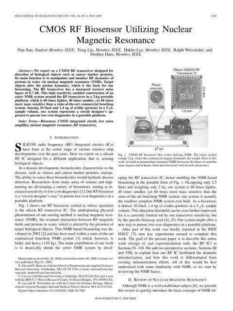
Fig. 1 shows our <strong>RF</strong> biosensor, central to whose operation<br />
is the silicon <strong>RF</strong> transceiver IC. The underpinning physical<br />
phenomenon of our sensing method is nuclear magnetic resonance<br />
(NMR), the resonant interaction between <strong>RF</strong> magnetic<br />
fields and protons in water, which is altered by the presence of<br />
target biological objects. This NMR-based biosensing was developed<br />
in 2002 [2] and has been used within a state-of-the-art<br />
commercial benchtop NMR system [3] which, however, is<br />
bulky and heavy (120 kg). The main contribution of our work<br />
is to drastically shrink the entire NMR system by devel-<br />
Manuscript received July 28, 2008; revised December 08, 2008. Current version<br />
published May 01, 2009.<br />
N. Sun and D. Ham are with the School of Engineering and Applied Sciences,<br />
Harvard University, Cambridge, MA 02138 USA (e-mail: nansun@seas.harvard.edu;<br />
donhee@seas.harvard.edu).<br />
Y. Liu was with Harvard University, Cambridge, MA 02138 USA, and is now<br />
with the IBM T. J. Watson Research Center, Yorktown Heights, NY 10598 USA.<br />
H. Lee and R. Weissleder are with the Center for Systems Biology, Massachusetts<br />
General Hospital, Harvard Medical School, Boston, MA 02114 USA.<br />
Digital Object Identifier 10.1109/JSSC.2009.2017007<br />
Fig. 1. <strong>CMOS</strong> <strong>RF</strong> biosensor (this work) utilizing NMR. The entire system<br />
weighs 2 kg, where the commercial magnet dominates the weight. Prior to this<br />
work, we built an intermediate miniature NMR biosensor [4] where we used the<br />
same magnet and in-house fabricated microcoil with discrete electronics.<br />
oping the <strong>RF</strong> transceiver IC, hence enabling the NMR-based<br />
biosensing in the portable form of Fig. 1. Occupying only 2.5<br />
liters and weighing only 2 kg, our system is 60 times lighter,<br />
40 times smaller, yet 60 times more mass sensitive than the<br />
state-of-the-art benchtop NMR system: our system is actually<br />
the smallest complete NMR system ever built. As a biosensor,<br />
it detects 20 fmol, 1.4 ng of avidin (protein) in a 5 L sample<br />
volume. This detection threshold can be even further improved,<br />
for it is currently limited not by our transceiver sensitivity, but<br />
by the specific bioassay used [4], [5]. Our system might offer a<br />
new way to pursue low-cost diagnostics in a portable platform.<br />
After part of this work was briefly reported in the IEEE<br />
ISSCC [7], new key experiments ensued to complete this<br />
work. The goal of the present paper is to describe this entire<br />
work (design of, and experimentation with, the <strong>RF</strong> IC) in<br />
Sections IV–VII. We add two perspective sections, Sections III<br />
and VIII, to explain how our <strong>RF</strong> IC facilitated the dramatic<br />
miniaturization, and how this work is differentiated from<br />
existing miniaturization efforts. All of this would be best<br />
understood with some familiarity with NMR, so we start by<br />
reviewing the NMR basics.<br />
II. REVIEW OF NUCLEAR MAGNETIC RESONANCE<br />
Although NMR is a well-established subject [6], we provide<br />
this review to quickly introduce the basic concepts of NMR rel-<br />
0018-9200/$25.00 © 2009 IEEE
1630 IEEE JOURNAL OF SOLID-STATE CIRCUITS, VOL. 44, NO. 5, MAY 2009<br />
Fig. 2. (a) Water in a magnetic field B . (b) Excitation (top) and reception (bottom) phase in NMR. (c) Motion of magnetic moment M in NMR.<br />
evant to this work, so that readers less familiar with NMR can<br />
rapidly access the main contribution portion of this paper.<br />
A. <strong>Nuclear</strong> <strong>Magnetic</strong> <strong>Resonance</strong><br />
Atomic nuclei with spin act like tiny bar magnets. These nuclear<br />
magnets are the main actors in the NMR phenomenon. We<br />
explain NMR using protons, the simplest nuclei. Proton NMR<br />
is observed with as common a substance as water, for it contains<br />
numerous hydrogen atoms whose nuclei are protons.<br />
Let water be placed in a static magnetic field [Fig. 2(a)].<br />
After several seconds, the system reaches an equilibrium, where<br />
the proton magnets preferentially line up along the direction of<br />
, just like a compass needle lines up along the Earth’s field.<br />
Macroscopically, in the equilibrium, the water exhibits a magnetic<br />
moment along the direction of , which we take as<br />
the -axis. This equilibrium state is the lowest energy state the<br />
system assumes.<br />
Now if one wraps a coil around the water and sends an <strong>RF</strong><br />
current into the coil, one can produce an <strong>RF</strong> magnetic field<br />
across the water [Fig. 2(b), top], where and<br />
are the amplitude and angular frequency of the <strong>RF</strong> field. If is<br />
not the Larmor frequency, defined as<br />
where is a proton-specific constant yielding MHz<br />
for<br />
, the proton magnets stay indifferent to the<br />
<strong>RF</strong> field and remains along the -axis. But for ,<br />
proton magnets absorb energy from the <strong>RF</strong> field, raising the potential<br />
energy of by misaligning from with an increasing<br />
angle between them. In other words, is tipped<br />
away from the -axis. As shown at three time instants , ,<br />
and in Fig. 2(c), this downward motion of is superposed<br />
with a much faster precession of at the Larmor frequency<br />
about the -axis. Overall, exhibits a spiral downward motion,<br />
when absorbing energy from the <strong>RF</strong> field. This absorption of <strong>RF</strong><br />
energy at by the proton magnets is termed nuclear magnetic<br />
resonance (NMR). During the energy absorption, the time taken<br />
(1)<br />
for to enter the -plane [ ; , Fig. 2(c)] from its<br />
alignment along the axis [ ; ]is<br />
Typically , which is why the downward motion of<br />
(growth of ) is much slower than its precession at .<br />
How does one figure out if was tuned to and NMR<br />
took place? One can cease the <strong>RF</strong> transmission at ,<br />
connect the coil to an <strong>RF</strong> receiver, and observe the coil output<br />
after [Fig. 2(b), bottom]. If , NMR did not<br />
occur and stayed along the -axis. Thus, nothing registers<br />
at the receiver after .If , NMR took place<br />
during the <strong>RF</strong> field transmission and is in<br />
the -plane at [Fig. 2(c)]. After , there is no<br />
more <strong>RF</strong> field for protons to absorb energy from, and hence,<br />
will stay in the -plane, maintaining with a constant<br />
potential energy. 1 , however, continues to precess with<br />
about the axis in the plane. Therefore, the coil experiences<br />
a periodic magnetic flux variation that induces an <strong>RF</strong> voltage<br />
of frequency across the coil. registers at the <strong>RF</strong><br />
receiver. Note that the <strong>RF</strong> excitation is stopped at<br />
because in the -plane induces the largest signal across the<br />
coil.<br />
is actually an exponentially damped sinusoid [Fig. 2(c)]<br />
with characteristic decay time called . The damping arises<br />
because the precession of an individual proton magnet is randomly<br />
perturbed by tiny magnetic fields produced by nearby<br />
proton magnets (proton-proton interaction). Due to the perturbation,<br />
each proton precesses at but with its own phase noise.<br />
Consequently, precessions of a large number of individual protons,<br />
which were initially in phase, grow out of phase over time<br />
in the -plane. As phase coherence is lost, the vector sum<br />
of individual proton magnetic moments exponentially decays,<br />
yielding the damped signal. For water, 1 and the quality<br />
1 As mentioned, after several seconds, M will lose energy to the environment,<br />
aligning along B to reach equilibrium. The time considered here in the main<br />
text, however, is far shorter than the equilibrium restoration time.<br />
(2)
SUN et al.: <strong>CMOS</strong> <strong>RF</strong> BIOSENSOR UTILIZING NUCLEAR MAGNETIC RESONANCE 1631<br />
Fig. 3. (a) T damping due to the basic proton-proton interaction. (b) T<br />
damping due to the static magnetic field inhomogeneity. (c) Echo technique.<br />
factor of the damped sinusoid with MHz<br />
is about .<br />
Through the NMR experiments described above, one obtains<br />
the values for and , which carry information on the compositions<br />
and properties of the substances in study. In this way,<br />
NMR has found applications in fields such as chemical spectroscopy,<br />
medical imaging (MRI), and biosensing.<br />
B. Echo Technique<br />
We have so far assumed a uniform static magnetic field<br />
across the water. In this case, all protons precess at the same frequency<br />
with phase noise caused by proton-proton interactions,<br />
yielding the -damped sinusoid at the receiver<br />
[Fig. 3(a)]. In reality, any magnet suffers a spatial variation of<br />
the field magnitude around the intended value . When such<br />
field inhomogeneity is present, is damped much faster with<br />
decay time , overriding the damping [Fig. 3(b)]. The faster<br />
damping arises because protons at different positions precess<br />
at different Larmor frequencies due to the field inhomogeneity,<br />
making them rapidly grow out of phase. To estimate ; assume<br />
that the field inhomogeneity is 50 parts per million (ppm)<br />
around . If we denote this fractional variation as ,<br />
then the precession frequencies range from<br />
to<br />
, and hence, the damped sinusoid of Fig. 3(b)<br />
has a bandwidth of around . Thus,<br />
,or 200 s 1 :<br />
even with 50 ppm inhomogeneity, the -damping completely<br />
masks the -damping.<br />
Since field inhomogeneity is deterministic, one can effectively<br />
remove the damping. Such a technique is important,<br />
as , which carries useful information, would be immeasurable<br />
otherwise. Fig. 3(c) illustrates one widely used technique<br />
[6]. The <strong>RF</strong> pulse is followed by repeated <strong>RF</strong> transmissions,<br />
each of duration . After the initial pulse, the<br />
proton magnets brought down to the -plane precess at different<br />
Larmor frequencies: those at a stronger field position<br />
precess faster and ahead of those at a weaker field position,<br />
resulting in the damping [ , Fig. 3(c)]. Now the<br />
pulse performs the same function as the pulse, but twice,<br />
Fig. 4. NMR-based biosensing [2].<br />
changing by 180 . Thus, after the pulse, the proton magnets<br />
return to the -plane, but with the faster precessing protons<br />
now lagging the slower ones (this inversion in relative positions<br />
may be difficult to grasp without detailed explanation,<br />
but let us accept it and move on, as the goal here is to become<br />
familiar with basic characteristics of the resulting signal, ).<br />
The former will catch up the latter, regaining phase coherence,<br />
hence showing the growing sinusoid [ , Fig. 3(c)]. After all<br />
protons acquire the same phase, the faster precessing protons<br />
again get ahead of the slower ones, once again resulting in dephasing<br />
and the damping [ , Fig. 3(c)]. As the pulse<br />
repeats, multiple such “echoes” register at the receiver. Since<br />
damping arising from random proton-proton interaction cannot<br />
be removed, the envelope of the echoes slowly decays with ,<br />
allowing its measurement despite field inhomogeneity.<br />
C. NMR-Based Biosensing<br />
Consider detecting certain proteins (e.g., receptors of circulating<br />
cancer cells, or soluble cancer biomarker proteins such as<br />
VEGF, PSA, CEA, and AFP) in a blood sample. Nanoscale magnetic<br />
particles [8] coated with antibodies that specifically bind<br />
to the target proteins are suspended in the sample (Fig. 4). If the<br />
proteins exist, the magnetic particles self-assemble into clusters<br />
around the proteins [2]. This self-assembly can be detected by<br />
performing proton NMR: a significant portion of blood is water,<br />
so we may regard the blood sample as water containing many<br />
protons for our purpose.<br />
Fig. 4 illustrates the echo signal from precessing protons<br />
in water in three different cases. In Fig. 4(a), water with<br />
no magnetic particles yields due to the basic proton-proton<br />
interactions. Fig. 4(b) shows the case of water containing<br />
mono-dispersed magnetic particles in the absence of target<br />
proteins. The magnetic particles incessantly move around due<br />
to inevitable Brownian motion and produce fluctuating local<br />
magnetic fields, perturbing precessions of proton magnets<br />
and causing more phase noise than is expected from the basic<br />
proton-proton interactions. Thus, phase coherence is lost more<br />
rapidly, reducing . In Fig. 4(c), due to the presence of target
1632 IEEE JOURNAL OF SOLID-STATE CIRCUITS, VOL. 44, NO. 5, MAY 2009<br />
proteins, the magnetic particles self-assemble into larger magnets,<br />
which are even more efficient in increasing phase noise in<br />
the proton magnets’ precession, further accelerating dephasing,<br />
yielding the smallest . Thus, by monitoring , one can<br />
detect target objects [2].<br />
III. <strong>CMOS</strong> <strong>RF</strong> TRANSCEIVER IC DESIGN:<br />
CHALLENGES<br />
The NMR-based biosensing requires an NMR system that<br />
can faithfully measure . To this end, the 120 kg commercial<br />
benchtop system [3] [Section I] has been used. The main focus<br />
of this work is the drastic miniaturization of the NMR system,<br />
enabling the NMR-based biosensing in the portable form of<br />
Fig. 1. Here we describe challenges that lie in such miniaturization,<br />
and how we met them through our <strong>RF</strong> IC design.<br />
As seen in Fig. 2, any NMR system consists of a magnet,<br />
a coil, and an <strong>RF</strong> transceiver. By far the largest component is<br />
the magnet (e.g., the 120 kg weight of the benchtop system is<br />
largely due to a large magnet). Therefore, any effort to shrink an<br />
NMR system should start with using a small magnet. An NMR<br />
system with a small magnet, however, suffers from a reduced<br />
signal at the input of the receiver.<br />
To see this, we note that , induced in the coil due to the<br />
periodic variation of magnetic flux caused by the precession of<br />
, is proportional to the rate of change of flux, , and the<br />
total magnetization<br />
: the volume factors<br />
in here because is measured per unit volume. Since<br />
at room temperature 2 and ,wehave<br />
This equation explains why a small magnet yields a small<br />
. Firstly, in general a small magnet tends to produce a weak<br />
field , and is reduced with quadratic dependence on .<br />
Secondly, a smaller magnet exhibits a more pronounced field<br />
inhomogeneity. In the presence of field inhomogeneity, protons<br />
at different positions of the sample have different Larmor frequencies,<br />
and thus, they are excited at different frequencies. Although<br />
the <strong>RF</strong> pulse has other frequency components than<br />
due to its finite duration of , it still has a limited<br />
bandwidth 1 . Therefore, the pulse can efficiently<br />
excite only protons in the region where their Larmor frequencies<br />
fall within the bandwidth of the pulse. If the field inhomogeneity<br />
is increased with a smaller magnet, the spatial extent the<br />
pulse can excite is reduced, effectively reducing the sample<br />
volume in (3) thus decreasing , regardless of the physical<br />
sample size. One may increase the bandwidth of the excitation<br />
pulse by decreasing the signal duration , but this requires a<br />
larger [see (2)] and thus a larger transmitted signal power,<br />
which is electronically limited.<br />
In summary, with a small magnet, is substantially reduced<br />
and its detection requires a highly sensitive <strong>RF</strong> transceiver.<br />
For facile NMR experiments avoiding the stringent requirement<br />
for the <strong>RF</strong> transceiver, people have used large magnets,<br />
leading to the existing bulky NMR instrumentation.<br />
2 This well-established relation is derived from the Boltzmann’s law, which<br />
we will use without showing the derivation.<br />
(3)<br />
To achieve the drastic miniaturization, we took the opposite<br />
approach: we use a very small magnet the size of an adult fist<br />
(Fig. 1), and to detect the resulting, substantially reduced signal<br />
(amplitude: 130 nV; available power: 0.5 fW), we design<br />
a highly sensitive <strong>RF</strong> transceiver. By opting to use a very small<br />
magnet for miniaturization, we shifted the entire system design<br />
burden onto the <strong>RF</strong> transceiver design, which we successfully<br />
carried out. Furthermore, we integrated the <strong>RF</strong> transceiver onto<br />
a <strong>CMOS</strong> IC. As a very small, low cost magnet is used, the circuit<br />
integration makes sense: in a conventional system where a<br />
large, expensive magnet dominates the system size and cost, integration<br />
of the <strong>RF</strong> transceiver would hardly reduce either the<br />
system size or the cost.<br />
Our design also uses a planar microcoil on a glass substrate<br />
(Fig. 1), having in mind mass production of the coil via standard<br />
microfabrication techniques. As compared to commonly<br />
used solenoidal coils, the planar coil’s geometry does not allow<br />
effective induction of from precessing protons, which was<br />
partly the reason for the weak signal amplitude of 130 nV. Once<br />
again, we overcame this undesirable effect by the design of the<br />
highly sensitive <strong>RF</strong> transceiver.<br />
IV. <strong>CMOS</strong> <strong>RF</strong> TRANSCEIVER IC DESIGN:<br />
ARCHITECTURE<br />
Fig. 5 shows the architecture of our NMR <strong>RF</strong> transceiver IC,<br />
which we describe now. As our magnet has , the <strong>RF</strong><br />
design is based at the Larmor frequency of 21.3 MHz.<br />
A. Receiver Path<br />
Let us first focus on the receiver path in Fig. 5. The signal<br />
appearing at node is a weak echo signal whose available<br />
power is 0.5 fW. The bandwidth of the echo signal is determined<br />
by the faster -damping due to the field inhomogeneity, instead<br />
of the slower -damping due to the proton-proton interaction.<br />
As discussed in Section II-B, the bandwidth corresponding to<br />
the -damping is where signifies the fractional field<br />
inhomogeneity. As we have<br />
, the echo signal in the<br />
frequency domain (Fig. 5) is centered at the Larmor frequency<br />
21.3 MHz, with a bandwidth of kHz.<br />
The echo signal is amplified by a low noise amplifier, and<br />
then frequency down-converted using mixers and a local oscillator.<br />
Choosing the proper frequency for the local oscillator is<br />
a critical task in dealing with the weak echo signal. Let us denote<br />
the oscillator frequency as .If is set to zero, the<br />
down-converted signal at node is swamped by noise. On<br />
the other hand, if is too large, rejecting noise outside the signal<br />
bandwidth of 1.1 kHz after the frequency down-conversion is<br />
difficult, as it requires a high quality factor for the bandpass<br />
filter. Since the signal is very weak, rejecting out-of-band noise<br />
in order not to corrupt the signal-to-noise ratio (SNR) is a critical<br />
task. We select<br />
kHz, with which the down-converted<br />
signal is not centered at , but very close to (Fig. 5),<br />
facilitating out-of-band noise rejection using a bandpass filter<br />
with a moderate quality factor.<br />
As in any heterodyning receiver, image noise would add 3 dB<br />
to the receiver noise figure, unless suppressed. We incorporate<br />
an image rejection algorithm in the digital domain after the
SUN et al.: <strong>CMOS</strong> <strong>RF</strong> BIOSENSOR UTILIZING NUCLEAR MAGNETIC RESONANCE 1633<br />
Fig. 5.<br />
The architecture of our NMR <strong>RF</strong> transceiver IC.<br />
down-converted signal is digitized using analog-to-digital converters<br />
(ADCs) (Fig. 5). A Hilbert transformer shifts the phase<br />
of the signal down-converted by the quadrature-phase local oscillator<br />
by . Addition of the Hilbert transformer output to<br />
the signal down-converted by the in-phase local oscillator nulls<br />
image noise.<br />
B. Transmitter Path<br />
Consider the transmitter path in Fig. 5. To produce the <strong>RF</strong><br />
magnetic field in the coil for excitation of proton magnets, we<br />
use the same local oscillator used for the frequency down-conversion<br />
in the receiver. The frequency of the local oscillator,<br />
, is not the Larmor frequency , but this arrangement is<br />
still effective in causing NMR, as we will explain shortly. The<br />
<strong>RF</strong> signal produced by the local oscillator is gated by the digital<br />
pulse generator, in order to generate the pulse followed by<br />
repeated pulses [Fig. 3(c)], which is to obtain the echo<br />
signal at the receiver.<br />
How can the pulse with the off-tuned frequency<br />
excite proton magnets in the sample? On one hand, the bandwidth<br />
of the pulse may be taken as 30% (15 kHz) of<br />
(shaded region in Fig. 6) centered about<br />
.On<br />
the other hand, across our 5 sample, the static field inhomogeneity<br />
is 50 ppm, and thus, the Larmor (excitation) frequencies<br />
of various positions of the sample range within the<br />
bandwidth of kHz (hashed region in Fig. 6)<br />
centered about<br />
. Combining, the entire<br />
sample is excited, as the range of the Larmor frequencies of<br />
the sample lies well within the bandwidth of the pulse.<br />
Of course, this scheme is possible because our sample is very<br />
small and the corresponding field inhomogeneity (and the resultant<br />
Larmor frequency variation) is relatively small.<br />
We could use a separate oscillator for the transmitter, but<br />
in such a scenario, we would have to tune the frequencies<br />
Fig. 6. Fourier transform of the T pulse with ! + excitation frequency.<br />
of both transmitter and receiver oscillators separately in the<br />
process of finding the frequency for NMR. In contrast, in our<br />
strategy sharing the same oscillator between the transmitter and<br />
receiver, we can just tune this single oscillator to find the right<br />
frequency for NMR, until the maximum signal appears at the<br />
output of the bandpass filter of Fig. 5.<br />
V. <strong>CMOS</strong> <strong>RF</strong> TRANSCEIVER IC DESIGN:<br />
FRONT-END DESIGN<br />
The planar microcoil (Fig. 1) is modeled as an inductor,<br />
nH, in series with parasitic resistance, (Fig. 5).<br />
Its quality is<br />
. Although the coil is inherently<br />
an inductor while a radio antenna assumes a 50 impedance,<br />
the coil is analogous to the antenna in that it emits power and<br />
picks up signals. Just like in radios, the matching of the transceiver<br />
to the coil and the low noise design of the receiver amplifier<br />
are crucial, especially in our case where is diminutive.<br />
Here we describe the front-end design.
1634 IEEE JOURNAL OF SOLID-STATE CIRCUITS, VOL. 44, NO. 5, MAY 2009<br />
Fig. 7. 50 impedance matching. (a) PA-coil. (b) LNA-coil.<br />
A. Power Matching<br />
The <strong>RF</strong> excitation pulses are sent to the coil through a<br />
power amplifier (PA). For maximum power transfer, the PA<br />
whose output impedance is (real number, e.g., 50 )is<br />
to be impedance matched to the coil. Two capacitors and<br />
arranged next to the coil in Fig. 7(a) form an impedance<br />
matching network widely used in NMR system design. With<br />
suitably chosen and , the real part of becomes<br />
while ’s inductive reactance is resonated out by , leading<br />
to .<br />
B. Noise Matching via Passive Amplification<br />
In the receiving stage of NMR experiments, the coil is connected<br />
to a low noise amplifier (LNA) to amplify the signal<br />
across the coil induced by precessing proton magnets. To minimize<br />
the noise figure, the LNA should be connected to the coil<br />
cautiously. In the widely practiced discrete design of the NMR<br />
<strong>RF</strong> transceiver, an off-the-shelf discrete LNA with a 50 input<br />
impedance is impedance matched to the coil using the same<br />
network discussed above. See Fig. 7(b), where<br />
in the coil’s model is the rms value of and is the<br />
power spectral density of the thermal noise generated by the<br />
coil’s resistance . This predominantly used strategy will work<br />
satisfactorily, as long as the LNA’s noise figure is small at the<br />
source impedance of 50 .<br />
Here we will seek a different LNA-coil connection option to<br />
obtain minimum noise figure, without demanding a priori either<br />
the 50 input impedance for the LNA or the impedance<br />
matching condition. To this end, consider a general passive network<br />
between the coil and the LNA [Fig. 8(a)]. The passive network<br />
has a voltage transfer function , which includes the<br />
effect of LNA’s input impedance, . Define .<br />
If noise in the passive network is ignored, or equivalently, if the<br />
passive network has negligible loss (this crucial assumption will<br />
be justified shortly), the passive network will “amplify” both<br />
the voltage signal and noise of the coil by the same factor ,<br />
while maintaining the SNR: at the output of the passive network,<br />
the signal is and the noise power spectral density<br />
is .<br />
If is large enough to put far beyond the LNA’s<br />
input referred noise [Fig. 8(b), left], the SNR is not<br />
degraded appreciably by the LNA, and the noise figure is small.<br />
In contrast, if is not large enough and is comparable<br />
to, or smaller than, [Fig. 8(b), right], the SNR<br />
is degraded considerably by the LNA, resulting in a high noise<br />
figure. Therefore, noise figure minimization entails two tasks:<br />
maximization of and minimization of the LNA’s input referred<br />
noise, . We defer the discussion of the second task till<br />
Section V-D, and here discuss how to maximize .<br />
We can immediately note that should be infinite to<br />
maximize , as any finite will only lower the voltage at<br />
the output of a given passive network. Now with ,we<br />
design a passive network that returns the maximum . Various<br />
topologies may be worked out, and here we use the network:<br />
Fig. 8(c). The aim is to choose and that maximize<br />
. should be infinite (short circuit), as any finite impedance<br />
in the path will lower the voltage at the passive network’s<br />
output. With , we choose that maximizes , which<br />
is given as a function of :<br />
where is the coil’s . becomes maximum<br />
when<br />
that is, when resonates with at .<br />
We have found that for a fixed LNA input referred noise, a<br />
shunt capacitor that resonates with the coil inductor at<br />
maximally amplifies the input signal and noise with a gain of<br />
, minimizing the noise figure. We assumed no noise (no loss)<br />
in the capacitor. This is to be justified, as any significant noise<br />
directly translates to noise figure, defeating the purpose of our<br />
technique. The assumption is indeed valid, for the quality factor<br />
of the capacitor is on the order of several hundreds, while the<br />
coil’s is 16. In this connection, the resonator in the minimum<br />
noise figure configuration may be understood as a passive<br />
preamplifier with a gain of 16 but with almost zero noise figure,<br />
which is unattainable with active amplifiers. Forming the<br />
resonator as a preamplifier naturally exploits the intrinsic inductor<br />
already available in the coil.<br />
Note that the minimum noise figure configuration does not<br />
involve impedance matching: the impedance looking into the<br />
passive network is , while [Fig. 8(c)]. Not the<br />
power, but the voltage is maximally delivered to the LNA, in<br />
achieving the minimum noise figure.<br />
Numerical examples may help appreciate this technique.<br />
The maximum amplitude of is 130 nV,<br />
thus<br />
. The noise generated in the coil is<br />
(4)<br />
(5)<br />
(6)
SUN et al.: <strong>CMOS</strong> <strong>RF</strong> BIOSENSOR UTILIZING NUCLEAR MAGNETIC RESONANCE 1635<br />
Fig. 8. (a) General passive network between a coil and an LNA. (b) Passively amplified signal and coil noise, and LNA’s input referred noise in frequency domain<br />
for a large (left) & small (right) . (c) Maximum passive amplification. (d) Maximum passive amplification in the presence of a transmission line.<br />
TABLE I<br />
LNA NOISE FIGURES FOR VARIOUS VALUES OF <br />
coil noise and LNA’s input referred noise. The point of our technique<br />
is to maximize the passively amplified coil noise so that<br />
it is far larger than LNA’s input referred noise.<br />
C. Generalization of Passive Amplification<br />
, and the input referred<br />
noise of our LNA is<br />
[Section V-D]. From these values, we created Table I where the<br />
passively amplified rms signal power , passively amplified<br />
coil noise over the signal bandwidth kHz ,<br />
, and LNA’s input referred noise over<br />
the bandwidth,<br />
, are given for three<br />
values of . For each , it also shows the noise figure, which<br />
was calculated using .<br />
From Table I, we note:<br />
• : In this optimum case [Fig. 8(c)], the passively<br />
amplified coil noise dominates the LNA’s input referred<br />
noise, yielding a noise figure of only 0.4 dB.<br />
• : This is the case where the coil is directly connected<br />
to the LNA with<br />
with no passive network.<br />
The LNA’s input referred noise dominates the passively<br />
amplified coil noise. Consequently, a large noise figure of<br />
14 dB results.<br />
• : If one uses the configuration of Fig. 7(b) with<br />
and yielding 50 but with an LNA with ,<br />
. This is a scenario where the network<br />
already designed for the impedance matching for the PA is<br />
directly connected to the LNA with . The noise<br />
figure is 4.9 dB.<br />
As seen, the noise figure varies substantially with ,asitdetermines<br />
the relative difference between the passively amplified<br />
As NMR transceivers have been realized mostly at the discrete<br />
level, the 50 matching with abundantly available 50<br />
off-the-shelf LNAs [Fig. 7(b)] has been the dominant choice<br />
for the LNA-coil connection. Regarding the resonance noise<br />
matching with the infinite impedance LNA [Fig. 8(c)], we suspected<br />
that this simple yet powerful technique might have been<br />
used during the 60 years of NMR, but there are very limited<br />
publications on the technique, and it is difficult to know the actual<br />
degree of its awareness and usage. It appears that the technique<br />
has been rarely conceived because custom design of an<br />
LNA (to produce non-50- impedance) is seldom exercised in<br />
the conventional discrete NMR system design. We found only<br />
two papers [9], [10] reporting the technique, where it was empirically<br />
demonstrated but with no explanation of its underlying<br />
machinery. We also found a patent [11] that discusses it, but<br />
wrongly disqualifies it as the optimum option. In this connection,<br />
our foregoing elucidation of the resonance noise matching<br />
may help its further recognition and appreciation, and clarify its<br />
concept.<br />
The reader may be concerned that the resonance noise<br />
matching may not work in the case the high impedance LNA<br />
is connected to a coil through a 50 coaxial cable [Fig. 8(d)],<br />
due to impedance mismatches at both ends of the line (this is a<br />
legitimate concern in that even at 21 MHz, a line length of, say<br />
20 cm, introduces a wave effect). This concern may be another<br />
reason for the dominance of the 50 matching: when a 50<br />
cable is used, “everything 50 ” offers the most convenient<br />
design choice. Contrary to the concern, however, the resonance
1636 IEEE JOURNAL OF SOLID-STATE CIRCUITS, VOL. 44, NO. 5, MAY 2009<br />
noise matching works well with a more general passive network<br />
containing a transmission line.<br />
To show this, let us work out the resonance noise matching in<br />
Fig. 8(d), based on our articulation of it from the previous subsection.<br />
The parameters of the transmission line are; characteristic<br />
impedance: , wave velocity: , length: , wave number:<br />
. We seek to find that maximizes for a fixed . Assume<br />
, although we can solve the problem generally.<br />
and in Fig. 8(d) are related through<br />
. The impedance is<br />
since<br />
. Therefore, the transmission line<br />
behaves like a capacitor<br />
at the coil end. Thus,<br />
to maximize , should resonate with at :<br />
The resulting maximum is again . This design is valid,<br />
as the line has a negligible measured loss (less than 0.05 dB for<br />
a 30 cm cable).<br />
(7)<br />
D. Design of the Low-Noise Amplifier<br />
As discussed in Section V-B, to minimize noise figure,<br />
should be maximized and the LNA’s input referred noise should<br />
be minimized. We have just discussed the former task. We now<br />
describe our LNA design to perform the latter. As<br />
is a prerequisite for maximum , a common source topology is<br />
chosen for the LNA. It has a capacitive input impedance, which<br />
may be regarded as infinite at low enough frequencies.<br />
Fig. 9 shows the schematic of our LNA. Since the design<br />
frequency, 21.3 MHz, is smaller than the noise corner<br />
( 50 MHz) of nMOS transistors in 0.18 m technology used,<br />
we use pMOS devices with the smaller noise corner ( 1<br />
MHz) [12] as input transistors and . pMOS transistors<br />
bring an additional benefit, the mitigation of the coupling of the<br />
substrate noise produced by the digital pulse generation circuits<br />
into the LNA input: the substrate noise would otherwise interfere<br />
with the weak signal at the LNA input, which is 4 even<br />
after the maximal passive amplification. On the same token,<br />
we must minimize the coupling of the strong local oscillator<br />
signal into the LNA input: it occurs first through the mixer,<br />
then, through the LNA’s input-output coupling capacitors. To<br />
minimize the latter coupling, cascode transistors and<br />
are used. Finally, to suppress the common mode noise, the<br />
amplifier is designed in a differential form and a common mode<br />
feedback circuit (CMFB) is employed. The capacitor and<br />
the resistor are for frequency compensation.<br />
With the arrangement above, the total noise of the LNA is<br />
dominated by the channel thermal noise of the transistors. The<br />
input referred noise of the LNA calculated through the standard<br />
small-signal analysis is given by<br />
where ( , 3 and 5) is the transistor ’s gate-source<br />
referred channel thermal noise. We have ignored the noise of<br />
the CMFB, and assumed perfectly matched differential pairs,<br />
to obtain the general guideline for how to size the transistors.<br />
(8)<br />
Fig. 9. LNA schematic.<br />
The third term is negligible as<br />
. To minimize the<br />
second term, active loads and are made much smaller<br />
than input transistors and : this leads to<br />
and the total input-referred noise is dominated by the first term,<br />
where is the transconductance of the<br />
input transistors. To reduce this first term, a large tail current (4<br />
mA) and wide input transistors (900 m) are used to maximize<br />
. From SPICE simulation, the input-referred noise of the<br />
LNA at 21.3 MHz is 1.3 and its voltage gain is 41 dB.<br />
Its input impedance, even with the wide input transistors, is still<br />
large enough at 21.3 MHz to guarantee .<br />
E. Comparison With the Inductively Source Degenerated LNA<br />
The passive amplification to minimize the noise figure is<br />
also employed in the inductively source degenerated LNA<br />
[Fig. 10(a)] widely used for wireless <strong>RF</strong> design [13], [14]<br />
although configured differently. As many designers are familiar<br />
with this LNA, here we compare it to our LNA.<br />
In the inductively source degenerated LNA of Fig. 10(a) designed<br />
for a wireless receiver, and are the input signal<br />
and noise from an antenna, while is the gate-source referred<br />
channel thermal noise of the transistor.<br />
is the antenna<br />
impedance. Inductors and and capacitor arranged<br />
around the transistor are chosen such that they resonate<br />
at the design frequency, and also present 50 to the antenna:<br />
in Fig. 10(a), . This 50 matching is<br />
required in wireless <strong>RF</strong> design, often reinforced by the band selection<br />
filter positioned between the antenna and the LNA. With<br />
such inductor and capacitor values, the network passively<br />
amplifies the input signal and noise, returning their amplified<br />
versions across the gate and source of the transistor [Fig. 10(b)]<br />
[13], [14]. The gain is , the effective
SUN et al.: <strong>CMOS</strong> <strong>RF</strong> BIOSENSOR UTILIZING NUCLEAR MAGNETIC RESONANCE 1637<br />
Fig. 10. (a) LNA with inductive source degeneration. (b) Passive amplification<br />
in this LNA. (c) Use of this LNA in Fig. 7(b).<br />
quality factor of the tank including the antenna resistance<br />
(the factor 2 is because ). If is large enough to put<br />
far beyond the transistor noise , the noise figure of<br />
the LNA will be small, as the SNR is minimally affected by the<br />
transistor noise. This is clearly the same passive amplification<br />
idea.<br />
Passive amplification is realized differently between our LNA<br />
[Fig. 8(c) or 9] and the inductively source degenerated LNA<br />
(Fig. 10). In the wireless <strong>RF</strong> design where 50 matching is required,<br />
the source degenerated LNA is well suited, as it simultaneously<br />
offers passive amplification and 50 matching. In<br />
contrast, NMR system design does not demand 50 matching.<br />
This, in conjunction with that the NMR coil has an inherent inductance,<br />
makes the implementation of passive amplification for<br />
NMR systems much simpler: the “free” inductor of the coil is<br />
used as an integral part of the passive amplifier, without<br />
adding extra inductors.<br />
Note that the inductively source degenerated LNA with a<br />
50 impedance can be used for the widely used 50 matched<br />
front-end of the NMR receiver [Fig. 7(b)]: such a design is<br />
shown in Fig. 10(c). Here although is only 1.7, the noise figure<br />
is small because the LNA’s input referred noise at node is significantly<br />
reduced, as it is the transistor’s gate-source referred<br />
channel thermal noise divided by : this is another way of<br />
looking at passive amplification in the source degenerated LNA.<br />
This design, however, does not exploit the free inductance of<br />
Fig. 11. Noise/power matching (a) with and (b) without a switch in the receiver<br />
path. (c) Transmitting mode. (d) Receiving mode.<br />
the coil. It instead transforms the coil impedance to 50 , then<br />
performs passive amplification, introducing extra inductors. Our<br />
design [Fig. 8(c) or 9] is thus a simpler choice as far as NMR<br />
system design is concerned.<br />
F. Simultaneous Noise and Power Matching<br />
We have seen that the receiver noise matching [Fig. 8(c)]<br />
and the transmitter power matching [Fig. 7(a)] require different<br />
passive networks. We may arrange the two networks<br />
separately, and to switch the coil to the LNA through the noise<br />
matching network during the receiving mode, and to the PA<br />
through the power matching network during the transmission<br />
mode [Fig. 11(a)]. This strategy, however, suffers from the loss<br />
associated with the switch. In the receiving mode, the turn-on<br />
loss of the switch will directly translates to noise figure.
1638 IEEE JOURNAL OF SOLID-STATE CIRCUITS, VOL. 44, NO. 5, MAY 2009<br />
To avoid the use of a switch in the receiving mode, we devised<br />
a new, differential matching network of Fig. 11(b). In the<br />
transmission mode, the switches next to the PA are turned on,<br />
and the PA is connected to the coil through the inductors<br />
and capacitors<br />
[Fig. 11(c)]. In the receiving mode,<br />
the switches are off, effectively making the inductors disappear,<br />
and the LNA is connected to the coil, whose impedance is modified<br />
by the capacitors<br />
[Fig. 11(d)]. The first point<br />
of this circuit is that the LNA in the receiving mode and the PA<br />
in the transmitting mode see two different impedances, that is,<br />
in Fig. 11. Thus, one can choose capacitors<br />
and inductors appropriately to provide power matching for the<br />
PA and noise matching for the LNA. Note that the difference<br />
between and arises not merely from the fact that<br />
the transmitting path has additional inductors, but more importantly<br />
from the fact that the impedance of the network of capacitors<br />
and the coil seen from the left is completely different from<br />
that seen from the right, that is,<br />
in Fig. 11. The<br />
second point is that neither lossy switches nor lossy inductors<br />
are present in the receiving mode [Fig. 11(d)], and hence, the<br />
matching network hardly degrades the receiver noise figure.<br />
We now consider how to select capacitor and inductor values<br />
quantitatively. For simplicity, we introduce the following notation:<br />
, , , and<br />
. in Fig. 11(d) is given by<br />
that is, when seen from the coil, the capacitors in Fig. 11(d)<br />
behave like one effective capacitor, whose impedance is to the<br />
right of the symbol. The noise matching condition [see (6)]<br />
for is that the effective capacitor resonates with at .<br />
This condition may be written as<br />
In the transmitting mode,<br />
of Fig. 11(c) is expressed as<br />
(9)<br />
(10)<br />
(11)<br />
For power matching, the real part of should equal the<br />
output resistance of the PA, while its capacitive reactance<br />
is to be resonated out by the inductors :<br />
(12)<br />
(13)<br />
If three conditions (10), (12) and (13) are simultaneously met,<br />
noise and power matching are simultaneously obtained. Since<br />
there are four unknown design parameters ( , , , and ),<br />
we have a large degree of freedom in choosing them.<br />
VI. <strong>CMOS</strong> <strong>RF</strong> TRANSCEIVER IC DESIGN:<br />
OTHER CIRCUIT CONSIDERATIONS<br />
A. Receiver Linearity<br />
Although the planar microcoil is the ultimate part of our<br />
system, it is desirable for the system to be able to accommodate<br />
a variety coils for varying experimental needs. The coil’s<br />
varies widely depending on its geometry and construction:<br />
e.g., while for the planar microcoil, for a<br />
solenoidal microcoil we built. The signal grows with the coil<br />
, especially with the resonance noise matching. To provide<br />
more amplification for a smaller signal, but to ensure that a<br />
larger signal does not enter the nonlinear regime of the mixer, 3<br />
we designed a variable gain amplifier (VGA) following the<br />
LNA (Fig. 5). The receiver linearity is important, as we seek to<br />
accurately extract .<br />
The VGA is depicted in the middle of Fig. 12. It is a differential<br />
common source amplifier with two tunable loads<br />
shown within the two dashed boxes. The VGA’s gain is altered<br />
by tuning the load impedance. Each load has three branches<br />
in parallel. Consider the branch built around transistor .<br />
As the control voltage is increased from zero, the operation<br />
regime of undergoes transitions from turn-off to<br />
pinch-off to triode, decreasing its drain-source resistance,<br />
. Therefore, the first branch serves as a<br />
voltage-controlled load. The second branch behaves essentially<br />
the same way, with decreasing of with increasing ,<br />
but this time, the gate of sees a voltage lower than due to<br />
, thus, the impedance-versus- curve for the second branch<br />
is that for the first branch, but translated along the axis. The<br />
third branch involving three transistors, , , and , also<br />
exhibits the same impedance-versus- curve, but even more<br />
shifted along the axis. By combining the three branches in<br />
parallel, the load impedance is tuned more smoothly over a<br />
wider range of , as compared to the case any single branch is<br />
used alone. The voltage gain tuning range of the VGA is from<br />
0.8 to 22. The VGA’s noise hardly contributes to the receiver<br />
noise figure, as the LNA’s gain is large (41 dB). Therefore, little<br />
noise minimization effort is required for the VGA.<br />
B. RX-TX Switching Scheme<br />
As discussed in Section V-F, to avoid the use of lossy switches<br />
in front of the LNA, in our design the LNA stays connected to<br />
the coil during the and pulse transmissions, e.g.,<br />
Fig. 11(b). In this approach, the large <strong>RF</strong> signal from the PA<br />
will saturate the receiver during the transmission mode. If the<br />
receiver is saturated during the transmission mode, restoration<br />
to its normal operation at the transition to the receiving phase<br />
(e.g., at ) will exhibit a settling behavior over the characteristic<br />
time of the receiver, compromising the initial reception<br />
of the signal.<br />
To address this issue, during the transmission mode, we reduce<br />
the gain of the LNA by closing switch in Fig. 12, preventing<br />
its saturation, and disconnect the rest of the receiver<br />
from the LNA by opening switches and of Fig. 12. Although<br />
and lie in the <strong>RF</strong> signal path, they come after the<br />
3 The input to our mixer can be as large as 10 mV within 5% gain reduction.
SUN et al.: <strong>CMOS</strong> <strong>RF</strong> BIOSENSOR UTILIZING NUCLEAR MAGNETIC RESONANCE 1639<br />
Fig. 12.<br />
Schematics of the LNA, VGA, and mixer, and their connections through a set of switches.<br />
LNA substantially amplifies the signal, thus, their turn-on resistances<br />
hardly contribute to the overall noise figure. Since<br />
and are not perfect switches and some of the large <strong>RF</strong> signal<br />
could leak to the VGA via their parasitic capacitors during the<br />
transmission mode, we also place switch to reduce the VGA<br />
gain during the transmission phase, and switches and to<br />
cut-off the mixer from the VGA.<br />
C. Mixer<br />
As shown at the left of Fig. 12, we use a double-balanced active<br />
mixer. Although the <strong>RF</strong> signal is down-converted to a low<br />
frequency of kHz, noise in the mixer does<br />
not interfere with the down-converted signal to any significant<br />
degree because the signal is amply amplified before the mixer<br />
and the LO generates a square wave. This is quantitatively confirmed,<br />
resorting to the study in [15]. The voltage gain of the<br />
mixer is 26 dB. The cascode transistors and are used<br />
to mitigate the undesired feed through from the LO to the LNA’s<br />
input path, which could otherwise interfere with the weak signal<br />
from the coil.<br />
VII. EXPERIMENTS<br />
We implemented the NMR transceiver in 0.18 m <strong>CMOS</strong><br />
technology. The IC occupies an area of 2.0 mm by 1.9 mm<br />
(Fig. 1). It contains, among components of Fig. 5, digital<br />
circuits for the pulse transmission, and most components associated<br />
with the heterodyning, that is, the LNA, VGA, mixers,<br />
and local oscillators including the frequency dividers. The<br />
matching network, PA, and ADCs were implemented with<br />
discrete components.<br />
As we deal with weak echo signals, the most important<br />
aspect of our design is the receiver noise figure, which we<br />
obtained by directly measuring the receiver input referred<br />
noise. After feeding an <strong>RF</strong> signal to the receiver input (node<br />
, Fig. 5), we measured the output at node using a spectrum<br />
analyzer. From this, we extracted the gain and output<br />
noise of the receiver. By dividing the output noise by the gain<br />
while factoring out image noise, we obtained the input referred<br />
noise of 1.8 . Since the LNA has a voltage gain of<br />
41 dB, the input referred noise is primarily contributed by the<br />
LNA. This measured input referred noise is larger than the<br />
SPICE-simulated value of 1.3 . The extra amount<br />
originates mostly from the power supply and substrate noise,<br />
which were not taken into account in the simulation.<br />
From the measured input referred noise and the measured<br />
impedance of the coil, we obtain the noise figure of the receiver.<br />
For the resonance noise matching with [Fig. 8(c)],<br />
the noise figure is only 0.7 dB. If we use the configuration<br />
of Fig. 8(c) but with and arranged for 50 matching,<br />
and the noise figure is 7.0 dB. These results agree<br />
well with our time domain measurements of the echo signal. For<br />
, we averaged 64 echo signals to obtain a clean echo<br />
signal. In contrast, for the resonance matching with ,<br />
only 4 time averaging was sufficient to obtain a clean echo<br />
signal, from which we were able to reliably extract . This is<br />
an unequivocal proof of substantial reduction of the noise figure<br />
via the maximum passive amplification.<br />
We assembled the entire NMR system of Fig. 1 by putting<br />
together the <strong>RF</strong> IC with auxiliary electronics on the printed circuit<br />
board, along with the planar microcoil and the magnet. The<br />
magnet and planar microcoil shown in Fig. 1 are borrowed from<br />
another work of ours [4], where the microcoil and its interface<br />
with sample were fully developed with extensive biosensing<br />
experiments but the electronics were at the discrete level with<br />
lower sensitivity and larger size. The magnet is a commercial<br />
product. The planar microcoil was in-house fabricated using<br />
standard photolithography. A 5 water sample is held on the<br />
microcoil inside a microfluidic container fabricated on top. In<br />
the following, we present NMR and biosensing experiments performed<br />
with the system.<br />
A. NMR Experiments<br />
We first performed proton NMR experiments in a phosphate<br />
buffered saline (PBS) solution, which is essentially biocompatible<br />
water. The top of Fig. 13 shows a down-converted echo<br />
signal measured at the output of the ADC of Fig. 5, which is
1640 IEEE JOURNAL OF SOLID-STATE CIRCUITS, VOL. 44, NO. 5, MAY 2009<br />
Fig. 14.<br />
Measured 1=T versus magnetic nanoparticle concentration in PBS.<br />
Fig. 13. Measured, down-converted echo signals: (top) pure PBS; (bottom)<br />
PBS with magnetic nanoparticles (0.17 mM).<br />
directly interfaced with a computer. From the exponentially decaying<br />
envelope of the echoes, shown as a dotted line, we extract<br />
. The repeated large spikes are coupling<br />
of the transmitted <strong>RF</strong> sequence through unidentified coupling<br />
paths, but they do not compromise the observation of the conspicuous<br />
echo signal, as they occur at different times. As magnetic<br />
nanoparticles [Fe] (diameter: 30 nm) are suspended in the<br />
PBS with a concentration of 0.17 mM, the measured is decreased<br />
to 60 ms (Fig. 13, bottom), as discussed in Section II-C.<br />
We remark that the data presented here and in what follows<br />
were obtained using an external signal generator instead of the<br />
on-chip local oscillator. Although the on-chip oscillator yielded<br />
echo signals from which values could be extracted, they were<br />
noisier as the on-chip oscillator was a free running oscillator.<br />
We discussed that decreases ( increases) with<br />
an increasing concentration of the magnetic nanoparticles<br />
[Section II-C]. The NMR theory tells more specifically that<br />
increases linearly with the concentration [16]. Measured<br />
with a varying concentration of the magnetic particles<br />
in Fig. 14 conform to the theory, affirming our system’s<br />
functionality.<br />
While the planar microcoil used to obtain Fig. 13<br />
was ultimately part of our system due to its fabrication advantage,<br />
we performed NMR experiments using a highersolenoidal<br />
microcoil<br />
to show the echo signals<br />
more clearly, far beyond the spikes, as shown in Fig. 15. As<br />
the magnetic particle concentration changes from 0.1 mM to<br />
1 mM, is reduced from 150 ms to 15 ms.<br />
Fig. 15. Measured, down-converted echo signals for two different concentrations<br />
of magnetic nanoparticles; with a solenoidal microcoil.<br />
B. Biomolecular Sensing<br />
Our NMR system with the planar microcoil can be used to<br />
sense biomolecules, as described in Section II-C. Consider, for<br />
example, the detection of avidin (protein) in the PBS. <strong>Magnetic</strong><br />
nanoparticles with surfaces coated with biotin (vitamin<br />
H) that specifically bind to avidin are suspended in the sample<br />
(Fig. 16). When avidin was absent in the sample, the magnetic<br />
particles were mono-dispersed, yielding of 73 ms (Fig. 16,<br />
top). When avidin existed in the sample with concentration of<br />
320 nM, the magnetic particles self-assembled into clusters [2],<br />
reducing to 31 ms (Fig. 16, bottom), thus indicating the presence<br />
of avidin.<br />
We repeated the experiment with a decreasing concentration<br />
of the avidin. The minimum detectable quantity of avidin was<br />
20 fmol and 1.4 ng in the 5 L sample volume (Fig. 17). In<br />
comparison to the state-of-the-art commercial benchtop NMR
SUN et al.: <strong>CMOS</strong> <strong>RF</strong> BIOSENSOR UTILIZING NUCLEAR MAGNETIC RESONANCE 1641<br />
TABLE II<br />
NMR SYSTEM MINIATURIZATION EFFORTS<br />
Fig. 16.<br />
Experimental avidin detection.<br />
For the works that (partially) integrated the transceiver [9],<br />
[18]–[20], none of them performed the NMR experiment with<br />
the small magnet that would substantially reduce the NMR<br />
signal as in our case, and thus, the circuit performance optimization<br />
was not the major issue. The integration level in [9],<br />
[19], [20] is low. The integration level in [18] is the highest<br />
among them, and this work represents a significant advance<br />
in art. Their target application is the measurement of various<br />
magnetic field strengths, and due to the difficulty of broadband<br />
noise matching, they directly connected their LNA to the coil<br />
with , inevitably degrading the noise figure performance.<br />
Overall, in terms of the entire system size, integration level,<br />
and circuit performance, our work is a step forward from the<br />
existing NMR miniaturization works.<br />
Fig. 17. Measured 1T for various avidin concentrations.<br />
system [3], our system is 60 times more sensitive in terms of<br />
the absolute detectable quantity (20 fmol), thus, our system is<br />
far more advantageous in desired mass-limited sensing applications.<br />
Even a better detection threshold can be attained via improvement<br />
in the bioassay, for our current detection threshold is<br />
limited not by our transceiver, but by the specific bioassay used<br />
[4], [5]. We also successfully carried out the detection of another<br />
biomolecule, folic acid, whose presentation is omitted here due<br />
to page limitation.<br />
For more extensive biosensing experiments, we refer readers<br />
to another work of ours in [4], where the same magnet and planar<br />
microcoil are used while the transceiver electronics are implemented<br />
in a discrete form with a lower receiver sensitivity.<br />
VIII. COMPARISON TO OTHER MINIATURIZATION WORKS<br />
Before concluding, we compare this work to other NMR<br />
system miniaturization efforts [4], [9], [17]–[20]. As shown<br />
in Table II, these works miniaturized only parts of the NMR<br />
system, but not the entire NMR system as we did. Thus, they<br />
are all much larger than our system.<br />
IX. CONCLUSION<br />
Combining <strong>RF</strong> microelectronics and biotechnology in the<br />
unifying framework of NMR, this work showcases how silicon<br />
<strong>RF</strong> ICs can be used not only for cell phones, but also<br />
for biosensing aimed at improving human health care. The<br />
portable, low-cost NMR system, made possible by the development<br />
of the highly sensitive <strong>CMOS</strong> <strong>RF</strong> transceiver with a<br />
noise figure of 0.7 dB, is an addition to the growing library of<br />
emerging biosensors aimed at early disease diagnosis and/or<br />
at personalized medical care. We are now developing an even<br />
smaller, handheld NMR system by using an even smaller<br />
magnet: this increases the associated burden on the transceiver<br />
IC design, thus more joy for circuit designers.<br />
ACKNOWLEDGMENT<br />
The authors thank M. Cole of Oxford University, W. Hill,<br />
W. Andress, and K. Donoghue of Harvard University, and<br />
D. Ricketts of Carnegie Mellon University for their valuable<br />
suggestions.<br />
REFERENCES<br />
[1] D. Ham and R. M. Westervelt, “The silicon that moves and feels small<br />
living things,” IEEE Solid-State Circuits Society Newsletter, vol. 12,<br />
no. 4, pp. 4–9, Oct. 2007, Fall issue.<br />
[2] J. M. Perez, L. Josephson, T. O’Loughlin, D. Hoegeman, and R.<br />
Weissleder, “<strong>Magnetic</strong> relaxation switches capable of sensing molecular<br />
interactions,” Nature Biotechnology, vol. 20, pp. 816–820, Aug.<br />
2002.<br />
[3] [Online]. Available: http://www.brukeroptics.com/minispec.html<br />
[4] H. Lee, E. Sun, D. Ham, and R. Weissleder, “Chip-NMR biosensor for<br />
detection & molecular analysis of cells,” Nature Medicine, vol. 14, no.<br />
8, pp. 869–874, Aug. 2008.
1642 IEEE JOURNAL OF SOLID-STATE CIRCUITS, VOL. 44, NO. 5, MAY 2009<br />
[5] I. Koh, R. Hong, R. Weissleder, and L. Josephson, “Sensitive NMR<br />
sensors detect antibodies to infuenza,” Angew. Chem. Int. Ed. Engl.,<br />
vol. 47, no. 22, pp. 4119–4121, 2008.<br />
[6] D. Canet, <strong>Nuclear</strong> <strong>Magnetic</strong> <strong>Resonance</strong>: Concepts and Methods.<br />
New York: Wiley, 1996.<br />
[7] Y. Liu, N. Sun, H. Lee, R. Weissleder, and D. Ham, “<strong>CMOS</strong> mini nuclear<br />
magnetic resonance system and its application for biomolecular<br />
sensing,” in IEEE Int. Solid-State Circuits Conf. Dig. Tech. Papers, Feb.<br />
2008, pp. 140–141.<br />
[8] H. Lee, Y. Liu, R. M. Westervelt, and D. Ham, “IC/microfluidic hybrid<br />
system for magnetic manipulation of biological cells,” IEEE J. Solid-<br />
State Circuits, vol. 41, no. 6, pp. 1471–1480, Jun. 2006.<br />
[9] T. Cherifi et al., “A <strong>CMOS</strong> microcoil-associated preamplifier for<br />
NMR spectroscopy,” IEEE Trans. Circuits Syst. I, vol. 52, no. 12, pp.<br />
2576–2583, Dec. 2005.<br />
[10] R. Meller and D. Hartill, “Pulsed NMR magnetometers for CESR,” in<br />
Proc. Particle Accelerator Conf., 2003, pp. 2339–2341.<br />
[11] “Signal/noise ratio optimization tuning system,” U.S. patent 5,347,222,<br />
Sep. 13, 1994.<br />
[12] D. M. Binkley, J. M. Rochelle, B. K. Swann, L. G. Clonts, and R. N.<br />
Goble, “A micropower <strong>CMOS</strong> direct-conversion, VLF receiver chip<br />
for magnetic-field wireless applications,” IEEE J. Solid-State Circuits,<br />
vol. 33, no. 3, pp. 344–358, Mar. 1998.<br />
[13] T. H. Lee, The Design of <strong>CMOS</strong> Radio-Frequency Integrated Circuits.<br />
Cambridge, MA: Cambridge Univ. Press, 1998.<br />
[14] D. K. Shaeffer and T. H. Lee, “A 1.5-V, 1.5-GHz <strong>CMOS</strong> low noise<br />
amplifier,” IEEE J. Solid-State Circuits, vol. 32, no. 5, pp. 745–759,<br />
May 1997.<br />
[15] H. Darabi and A. A. Abidi, “Noise in <strong>RF</strong>-<strong>CMOS</strong> mixers: A simple<br />
physical model,” IEEE J. Solid-State Circuits, vol. 35, no. 1, pp. 15–25,<br />
Jan. 2000.<br />
[16] A. Roch, R. N. Muller, and P. Gillis, “Theory of proton relaxation induced<br />
by superparamagnetic particles,” J. Chem. Phys., vol. 110, no.<br />
11, pp. 5403–5411, Mar. 1999.<br />
[17] G. Eidmann, R. Savelsberg, P. Blümler, and B. Blümich, “The NMR<br />
mouse, a mobile universal surface explorer,” J. Magn. <strong>Resonance</strong>, ser.<br />
Series A, vol. 122, pp. 104–109, 1996.<br />
[18] G. Boero et al., “Fully integrated probe for proton nuclear magnetic resonance<br />
magnetometry,” Rev. Sci. Instruments, vol. 72, pp. 2764–2768,<br />
Jun. 2001.<br />
[19] L. Fan et al., “Miniaturization of magnetic resonance microsystem<br />
components for 3-D cell imaging,” in IEEE ISSCC Dig. Tech. Papers,<br />
Feb. 2007, pp. 166–167.<br />
[20] R. Magin et al., “Miniature magnetic resonance machines,” IEEE Spectrum,<br />
p. 51, Oct. 1997.<br />
Yong Liu (S’03–M’07) received the B.S. and M.S.<br />
degrees from Tsinghua University, Beijing, China, in<br />
2000 and 2003, and the Ph.D. degree from Harvard<br />
University, Cambridge, MA, in 2007, all in electrical<br />
engineering. He is currently with the IBM T. J.<br />
Watson Research Center, Yorktown Heights, NY.<br />
His Ph.D. work examined applications of <strong>CMOS</strong><br />
ICs in medicine and biotechnology, by directly<br />
interfacing <strong>CMOS</strong> ICs with biological systems.<br />
Specifically, his work consisted of two projects.<br />
First, he developed <strong>CMOS</strong> ICs in conjunction with<br />
microfluidic systems to magnetically manipulate individual biological cells for<br />
cell sorting applications. Second, he developed a <strong>CMOS</strong> <strong>RF</strong> biosensor utilizing<br />
NMR for medical diagnostics in a portable platform. Additionally, he worked<br />
on <strong>RF</strong> and mixed-signal ICs for communication and computation systems<br />
during his stay at Harvard, including autonomic PLLs for multi-domain<br />
synchronous clocking. His current research at IBM is on wireline transceiver<br />
design. He has 14 publications, two U.S. patents, and three provisional patents<br />
filed.<br />
In 2001, he was with Tsinghua Tongfang Microelectronics Co., working on<br />
the second-generation Chinese <strong>RF</strong> ID card. In 2005 and 2006, he was with the<br />
Mixed-signal Communications IC Group at IBM T. J. Watson Research Center<br />
as a summer intern. He was the recipient of the Seagate Scholarship, Motorola<br />
Scholarship, Second Prize in the China National Graduate EDA Competition,<br />
and Analog Devices Outstanding Student Designer Award. He is a co-winner of<br />
the Beatrice Editorial Excellence Award in the 2009 IEEE International Solid-<br />
State Circuits Conference (ISSCC).<br />
Hakho Lee (M’05) is an Instructor in Biomedical<br />
Engineering program at the Center for Systems Biology<br />
at the Massachusetts General Hospital (MGH)<br />
and Harvard Medical School (HMS). He received the<br />
Ph.D. degree in physics from Harvard University in<br />
2005, and joined the Center for Molecular Imaging<br />
Research at MGH/HMS as a Research Associate. He<br />
has contributed to developing a new type of micrototal-analysis-systems<br />
by combining integrated circuits<br />
and microfluidics and developed the miniature<br />
NMR system. Dr. Lee’s research topics include the<br />
synthesis of novel magnetic particles and the development of microelectronic<br />
systems for medical diagnosis.<br />
Nan Sun (S’06) received the B.S. degree in<br />
electrical engineering from Tsinghua University,<br />
Beijing, China, in 2006, where he ranked the top<br />
first out of 160 students in the Electrical Engineering<br />
Department every single year, and graduated with<br />
the highest honor and outstanding undergraduate<br />
thesis award. He is currently working towards the<br />
Ph.D. degree in electrical engineering at Harvard<br />
University, Cambridge, MA.<br />
His Ph.D. research is twofold. First, he has<br />
developed several <strong>CMOS</strong> <strong>RF</strong> biomolecular sensors<br />
utilizing nuclear magnetic resonance (NMR) to pursue early disease detection<br />
and low-cost medicine. These systems can be used not only for low-cost<br />
medical diagnostics, but also for oil detection and quantum computing on<br />
silicon. Second, he is developing digital background calibration techniques<br />
for pipelined analog-to-digital converters. In addition to these two works, he<br />
has also made a key contribution to proving the chaotic nature of uncontrolled<br />
soliton oscillators by performing a Lyapunov analysis.<br />
Mr. Sun received the first-class Tsinghua University Outstanding Student<br />
Award in each year from 2003 to 2006. He won the Top Prize in the Intercollegiate<br />
Physics Competition in 2003. He is the recipient of the Samsung Outstanding<br />
Student Award in 2003, Hewlett Packard Outstanding Student Award<br />
in 2006, and Analog Device Outstanding Student Designer Award in 2007. He<br />
won the Harvard Teaching Fellow Award in 2008. He has filed 4 US provisional<br />
patents.<br />
Ralph Weissleder is a Professor at Harvard Medical<br />
School, Director of the Center for Systems Biology<br />
at Massachusetts General Hospital (MGH), Director<br />
of the Center for Molecular Imaging Research,<br />
and Attending Clinician at MGH. Dr. Weissleder is<br />
also a member of the Dana Farber Harvard Cancer<br />
Center, an Associate Member of the Broad Institute<br />
(Chemical Biology Program), and a member of the<br />
Harvard Stem Cell Institute (HSCI). Dr. Weissleder’s<br />
research interests include the development of novel<br />
molecular imaging techniques, tools for detection of<br />
early disease detection and development of nanomaterials for sensing and systems<br />
analysis. His research has been translational and several of his developments<br />
have led to advanced clinical trials with anticipated major impacts when<br />
these methods become routinely available. He has published over 500 original<br />
publications in peer reviewed journals and has authored several textbooks. His<br />
work has been honored with numerous awards including the J. Taylor International<br />
Prize in Medicine, the Millennium Pharmaceuticals Innovator Award, the<br />
AUR Memorial Award, the ARRS President’s Award, the Society for Molecular<br />
Imaging Lifetime Achievement Award, the Academy of Molecular Imaging<br />
2006 Distinguished Basic Scientist Award, and the 2008 RSNA Outstanding Researcher<br />
Award.
SUN et al.: <strong>CMOS</strong> <strong>RF</strong> BIOSENSOR UTILIZING NUCLEAR MAGNETIC RESONANCE 1643<br />
Donhee Ham (S’99–M’02) is John L. Loeb Associate<br />
Professor of the Natural Sciences and Associate<br />
Professor of Electrical Engineering at Harvard University,<br />
Cambridge, MA, where he is with the School<br />
of Engineering and Applied Sciences (Programs:<br />
Electrical Engineering and Applied Physics).<br />
He received the B.S. degree in physics from<br />
Seoul National University, Korea, in 1996, where he<br />
graduated summa cum laude with the Valedictorian<br />
Prize as well as the Presidential Prize, ranked top 1st<br />
across the Natural Science College, and also with the<br />
Physics Gold Medal (sole winner). Following 1.5 years of mandatory military<br />
service in the Republic of Korea Army, he proceeded to California Institute of<br />
Technology, Pasadena, CA, where he received the M.S. degree in physics in<br />
1999 working on general relativity and gravitational astrophysics, and Ph.D.<br />
degree in electrical engineering in 2002 winning the Charles Wilts Doctoral<br />
Thesis Prize, Best thesis award in Electrical Engineering. His doctoral work<br />
examined the statistical physics of electrical circuits. He was the recipient of<br />
the IBM Doctoral Fellowship, IBM Faculty Partnership Award, IBM Research<br />
Design Challenge Award, Li Ming Scholarship, Silver Medal in National<br />
Math Olympiad, and the fellow of the Korea Foundation of Advanced Studies.<br />
He shared Harvard’s Hoopes prize with William Franklin Andress. He was<br />
recognized by MIT Technology Review as among the world’s top 35 young<br />
innovators in 2008 (TR35), for his group’s work on <strong>CMOS</strong> <strong>RF</strong> biomolecular<br />
sensor using nuclear spin resonance to pursue early disease detection and<br />
low-cost medicine.<br />
Dr. Ham’s work experiences include Caltech-MIT Laser Interferometer<br />
Gravitational Wave Observatory (LIGO), IBM T. J. Watson Research Center,<br />
IEEE conference technical program committees including the IEEE International<br />
Solid-State Circuits Conference (ISSCC) and the IEEE Asian Solid-State<br />
Circuits Conference (ASSCC), advisory board for the IEEE International Symposium<br />
on Circuits and Systems (ISCAS), international advisory board for the<br />
Institute for Nanodevices and Biosystems, and various U.S., Korea, and Japan<br />
industry, government, and academic technical advisory positions on subjects<br />
including ultrafast electronics, science and technology at the nanoscale, and the<br />
interface between biotechnology and microelectronics. He was a guest editor<br />
for the IEEE JOURNAL OF SOLID-STATE CIRCUITS (JSSC, January 2009) and a<br />
co-editor of <strong>CMOS</strong> Biotechnology with Springer (2007).<br />
The research focus of his research group at Harvard University is on: 1) <strong>RF</strong>,<br />
analog and mixed-signal ICs; 2) GHz/THz 1-dimensional electronic and plasmonic<br />
transport in quantum wires; 3) soliton and nonlinear wave electronics; 4)<br />
applications of <strong>CMOS</strong> ICs in biotechnology.