IEEE 1149.1 JTAG Boundary Scan
IEEE 1149.1 JTAG Boundary Scan
IEEE 1149.1 JTAG Boundary Scan

You also want an ePaper? Increase the reach of your titles
YUMPU automatically turns print PDFs into web optimized ePapers that Google loves.
<strong>IEEE</strong> <strong>1149.1</strong> <strong>JTAG</strong><br />
<strong>Boundary</strong> <strong>Scan</strong><br />
F<br />
o<br />
r<br />
m<br />
a<br />
t<br />
i<br />
o<br />
n<br />
s<br />
t<br />
e<br />
c<br />
h<br />
n<br />
i<br />
q<br />
u<br />
e<br />
s<br />
●<br />
●<br />
●<br />
●<br />
●<br />
●<br />
●<br />
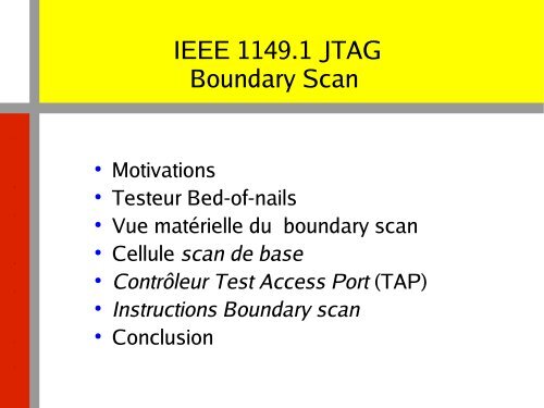
Motivations<br />
Testeur Bed-of-nails<br />
Vue matérielle du boundary scan<br />
Cellule scan de base<br />
Contrôleur Test Access Port (TAP)<br />
Instructions <strong>Boundary</strong> scan<br />
Conclusion
Bed Of Nails<br />
F<br />
o<br />
r<br />
m<br />
a<br />
t<br />
i<br />
o<br />
n<br />
s<br />
t<br />
e<br />
c<br />
h<br />
n<br />
i<br />
q<br />
u<br />
e<br />
s
Bed Of Nails<br />
F<br />
o<br />
r<br />
m<br />
a<br />
t<br />
i<br />
o<br />
n<br />
s<br />
t<br />
e<br />
c<br />
h<br />
n<br />
i<br />
q<br />
u<br />
e<br />
s
Motivations pour un Standard<br />
F<br />
o<br />
r<br />
m<br />
a<br />
t<br />
i<br />
o<br />
n<br />
s<br />
t<br />
e<br />
c<br />
h<br />
n<br />
i<br />
q<br />
u<br />
e<br />
s<br />
Bed-of-nails printed circuit board tester gone<br />
We put components on both sides of PCB & replaced DIPs<br />
with flat packs to reduce inductance<br />
Nails would hit components<br />
Reduced spacing between PCB wires<br />
Nails would short the wires<br />
PCB Tester must be replaced with built-in test delivery<br />
system -- <strong>JTAG</strong> does that<br />
Need standard System Test Port and Bus<br />
Integrate components from different vendors<br />
Test bus identical for various components<br />
One chip has test hardware for other chips
Concept des testeurs<br />
Bed-of-Nails<br />
F<br />
o<br />
r<br />
m<br />
a<br />
t<br />
i<br />
o<br />
n<br />
s<br />
t<br />
e<br />
c<br />
h<br />
n<br />
i<br />
q<br />
u<br />
e<br />
s
Testeur Bed-of-Nails<br />
F<br />
o<br />
r<br />
m<br />
a<br />
t<br />
i<br />
o<br />
n<br />
s<br />
t<br />
e<br />
c<br />
h<br />
n<br />
i<br />
q<br />
u<br />
e<br />
s
Purpose of Standard<br />
F<br />
o<br />
r<br />
m<br />
a<br />
t<br />
i<br />
o<br />
n<br />
s<br />
t<br />
e<br />
c<br />
h<br />
n<br />
i<br />
q<br />
u<br />
e<br />
s<br />
Lets test instructions and test data be serially fed<br />
into a component-under-test (CUT)<br />
Allows reading out of test results<br />
Allows RUNBIST command as an instruction<br />
Too many shifts to shift in external tests<br />
<strong>JTAG</strong> can operate at chip, PCB, & system levels<br />
Allows control of tri-state signals during testing<br />
Lets other chips collect responses from CUT<br />
Lets system interconnect be tested separately from<br />
components<br />
Lets components be tested separately from wires
System Test Logic<br />
F<br />
o<br />
r<br />
m<br />
a<br />
t<br />
i<br />
o<br />
n<br />
s<br />
t<br />
e<br />
c<br />
h<br />
n<br />
i<br />
q<br />
u<br />
e<br />
s
Instruction Register Loading with<br />
<strong>JTAG</strong><br />
F<br />
o<br />
r<br />
m<br />
a<br />
t<br />
i<br />
o<br />
n<br />
s<br />
t<br />
e<br />
c<br />
h<br />
n<br />
i<br />
q<br />
u<br />
e<br />
s
System View of Interconnect<br />
F<br />
o<br />
r<br />
m<br />
a<br />
t<br />
i<br />
o<br />
n<br />
s<br />
t<br />
e<br />
c<br />
h<br />
n<br />
i<br />
q<br />
u<br />
e<br />
s
<strong>Boundary</strong> <strong>Scan</strong> Chain View<br />
F<br />
o<br />
r<br />
m<br />
a<br />
t<br />
i<br />
o<br />
n<br />
s<br />
t<br />
e<br />
c<br />
h<br />
n<br />
i<br />
q<br />
u<br />
e<br />
s
Elementary <strong>Boundary</strong> <strong>Scan</strong> Cell<br />
F<br />
o<br />
r<br />
m<br />
a<br />
t<br />
i<br />
o<br />
n<br />
s<br />
t<br />
e<br />
c<br />
h<br />
n<br />
i<br />
q<br />
u<br />
e<br />
s
Serial Board / MCM <strong>Scan</strong><br />
F<br />
o<br />
r<br />
m<br />
a<br />
t<br />
i<br />
o<br />
n<br />
s<br />
t<br />
e<br />
c<br />
h<br />
n<br />
i<br />
q<br />
u<br />
e<br />
s
Parallel Board / MCM <strong>Scan</strong><br />
F<br />
o<br />
r<br />
m<br />
a<br />
t<br />
i<br />
o<br />
n<br />
s<br />
t<br />
e<br />
c<br />
h<br />
n<br />
i<br />
q<br />
u<br />
e<br />
s
Independent Path Board / MCM<br />
<strong>Scan</strong><br />
F<br />
o<br />
r<br />
m<br />
a<br />
t<br />
i<br />
o<br />
n<br />
s<br />
t<br />
e<br />
c<br />
h<br />
n<br />
i<br />
q<br />
u<br />
e<br />
s
Tap Controller Signals<br />
F<br />
o<br />
r<br />
m<br />
a<br />
t<br />
i<br />
o<br />
n<br />
s<br />
t<br />
e<br />
c<br />
h<br />
n<br />
i<br />
q<br />
u<br />
e<br />
s<br />
■<br />
Test Access Port (TAP) includes these signals:<br />
Test Clock Input (TCK) -- Clock for test logic<br />
■ Can run at different rate from system clock<br />
Test Mode Select (TMS) -- Switches system from<br />
functional to test mode<br />
Test Data Input (TDI) -- Accepts serial test data and<br />
instructions -- used to shift in vectors or one of many<br />
test instructions<br />
Test Data Output (TDO) -- Serially shifts out test<br />
results captured in boundary scan chain (or device<br />
ID or other internal registers)<br />
Test Reset (TRST) -- Optional asynchronous TAP<br />
controller reset
Tap Controller State Diagram<br />
F<br />
o<br />
r<br />
m<br />
a<br />
t<br />
i<br />
o<br />
n<br />
s<br />
t<br />
e<br />
c<br />
h<br />
n<br />
i<br />
q<br />
u<br />
e<br />
s
Tap Controller Timing<br />
F<br />
o<br />
r<br />
m<br />
a<br />
t<br />
i<br />
o<br />
n<br />
s<br />
t<br />
e<br />
c<br />
h<br />
n<br />
i<br />
q<br />
u<br />
e<br />
s
TAP Controller Power-Up Reset<br />
Logic<br />
F<br />
o<br />
r<br />
m<br />
a<br />
t<br />
i<br />
o<br />
n<br />
s<br />
t<br />
e<br />
c<br />
h<br />
n<br />
i<br />
q<br />
u<br />
e<br />
s
F<br />
o<br />
r<br />
m<br />
a<br />
t<br />
i<br />
o<br />
n<br />
s<br />
<strong>Boundary</strong> <strong>Scan</strong> Instructions<br />
t<br />
e<br />
c<br />
h<br />
n<br />
i<br />
q<br />
u<br />
e<br />
s
SAMPLE / PRELOAD Instruction --<br />
SAMPLE<br />
F<br />
o<br />
r<br />
m<br />
a<br />
t<br />
i<br />
o<br />
n<br />
s<br />
Purpose:<br />
2. Get snapshot of normal chip output signals<br />
3. Put data on bound. scan chain before next instr.<br />
t<br />
e<br />
c<br />
h<br />
n<br />
i<br />
q<br />
u<br />
e<br />
s
SAMPLE / PRELOAD Instruction --<br />
PRELOAD<br />
F<br />
o<br />
r<br />
m<br />
a<br />
t<br />
i<br />
o<br />
n<br />
s<br />
t<br />
e<br />
c<br />
h<br />
n<br />
i<br />
q<br />
u<br />
e<br />
s
EXTEST Instruction<br />
F<br />
o<br />
r<br />
m<br />
a<br />
t<br />
i<br />
o<br />
n<br />
s<br />
t<br />
e<br />
c<br />
h<br />
n<br />
i<br />
q<br />
u<br />
e<br />
s<br />
■<br />
Purpose: Test off-chip circuits and board-level interconnections
INTEST Instruction<br />
■<br />
F<br />
o<br />
r<br />
m<br />
a<br />
t<br />
i<br />
o<br />
n<br />
s<br />
Purpose:<br />
1. Shifts external test patterns onto component<br />
2. External tester shifts component responses out<br />
t<br />
e<br />
c<br />
h<br />
n<br />
i<br />
q<br />
u<br />
e<br />
s
INTEST Instruction Clocks<br />
F<br />
o<br />
r<br />
m<br />
a<br />
t<br />
i<br />
o<br />
n<br />
s<br />
t<br />
e<br />
c<br />
h<br />
n<br />
i<br />
q<br />
u<br />
e<br />
s<br />
■<br />
■<br />
Control of applied system clock during INTEST<br />
Use of TCK for on-chip system logic clock
RUNBIST Instruction<br />
■<br />
F<br />
o<br />
r<br />
■<br />
m<br />
a■<br />
t<br />
i<br />
o<br />
n<br />
s<br />
■<br />
t<br />
e<br />
c<br />
h<br />
n<br />
i<br />
q<br />
u<br />
e<br />
s<br />
■<br />
Purpose: Allows you to issue BIST command to component through <strong>JTAG</strong><br />
hardware<br />
Optional instruction<br />
Lets test logic control state of output pins<br />
1. Can be determined by pin boundary scan cell<br />
2. Can be forced into high impedance state<br />
BIST result (success or failure) can be left in boundary scan cell or<br />
internal cell<br />
Shift out through boundary scan chain<br />
May leave chip pins in an indeterminate state (reset required before<br />
normal operation resumes)
CLAMP Instruction<br />
F<br />
o<br />
r<br />
m<br />
a<br />
t<br />
i<br />
o<br />
n<br />
s<br />
t<br />
e<br />
c<br />
h<br />
n<br />
i<br />
q<br />
u<br />
e<br />
s<br />
■<br />
■<br />
■<br />
■<br />
Purpose: Forces component output signals to be driven by<br />
boundary-scan register<br />
Bypasses the boundary scan chain by using the one-bit Bypass<br />
Register<br />
Optional instruction<br />
May have to add RESET hardware to control on-chip logic so<br />
that it does not get damaged (by shorting 0’s and 1’s onto an<br />
internal bus, etc.)
IDCODE Instruction<br />
F<br />
o<br />
r<br />
m<br />
a<br />
t<br />
i<br />
o<br />
n<br />
s<br />
t<br />
e<br />
c<br />
h<br />
n<br />
i<br />
q<br />
u<br />
e<br />
s<br />
■<br />
■<br />
■<br />
Purpose: Connects the component device identification register<br />
serially between TDI and TDO<br />
In the Shift-DR TAP controller state<br />
Allows board-level test controller or external tester to read out<br />
component ID<br />
Required whenever a JEDEC identification register is included<br />
in the design
Device ID Register --JEDEC<br />
Code<br />
F<br />
o<br />
r<br />
m<br />
a<br />
t<br />
i<br />
o<br />
n<br />
s<br />
t<br />
e<br />
c<br />
h<br />
n<br />
i<br />
q<br />
u<br />
e<br />
s<br />
MSB<br />
27 12<br />
Part<br />
Number<br />
(16 bits)<br />
11 1<br />
Manufacturer<br />
Identity<br />
(11 bits)<br />
LSB<br />
0<br />
‘1’<br />
(1 bit)
USERCODE Instruction<br />
F<br />
o<br />
r<br />
m<br />
a<br />
t<br />
i<br />
o<br />
n<br />
s<br />
t<br />
e<br />
c<br />
h<br />
n<br />
i<br />
q<br />
u<br />
e<br />
s<br />
●<br />
●<br />
●<br />
●<br />
●<br />
Purpose: Intended for user-programmable components<br />
(FPGA’s, EEPROMs, etc.)<br />
– Allows external tester to determine user programming<br />
of component<br />
Selects the device identification register as serially<br />
connected between TDI and TDO<br />
User-programmable ID code loaded into device<br />
identification register<br />
– On rising TCK edge<br />
Switches component test hardware to its system function<br />
Required when Device ID register included on userprogrammable<br />
component
HIGHZ Instruction<br />
F<br />
o<br />
r<br />
m<br />
a<br />
t<br />
i<br />
o<br />
n<br />
s<br />
t<br />
e<br />
c<br />
h<br />
n<br />
i<br />
q<br />
u<br />
e<br />
s<br />
■<br />
■<br />
■<br />
■<br />
Purpose: Puts all component output pin signals into high-impedance<br />
state<br />
Control chip logic to avoid damage in this mode<br />
May have to reset component after HIGHZ runs<br />
Optional instruction
BYPASS Instruction<br />
F<br />
o■<br />
r<br />
m<br />
a<br />
t<br />
i<br />
o<br />
n<br />
s<br />
Purpose: Bypasses scan chain with 1-bit register<br />
t<br />
e<br />
c<br />
h<br />
n<br />
i<br />
q<br />
u<br />
e<br />
s
Optional / Required Instructions<br />
F<br />
o<br />
r<br />
m<br />
a<br />
t<br />
i<br />
o<br />
n<br />
s<br />
t<br />
e<br />
c<br />
h<br />
n<br />
i<br />
q<br />
u<br />
e<br />
s<br />
Instruction<br />
BYPASS<br />
CLAMP<br />
EXTEST<br />
HIGHZ<br />
IDCODE<br />
INTEST<br />
RUNBIST<br />
SAMPLE / PRELOAD<br />
USERCODE<br />
Status<br />
Mandatory<br />
Optional<br />
Mandatory<br />
Optional<br />
Optional<br />
Optional<br />
Optional<br />
Mandatory<br />
Optional
Summary<br />
F<br />
o<br />
r<br />
m<br />
a<br />
t<br />
i<br />
o<br />
n<br />
s<br />
t<br />
e<br />
c<br />
h<br />
n<br />
i<br />
q<br />
u<br />
e<br />
s<br />
■ <strong>Boundary</strong> <strong>Scan</strong> Standard has become absolutely essential --<br />
No longer possible to test printed circuit<br />
boards with bed-of-nails tester<br />
Not possible to test multi-chip modules at all<br />
without it<br />
Supports BIST, external testing with<br />
Automatic Test Equipment, and boundary<br />
scan chain reconfiguration as BIST pattern<br />
generator and response compacter<br />
Now getting widespread usage