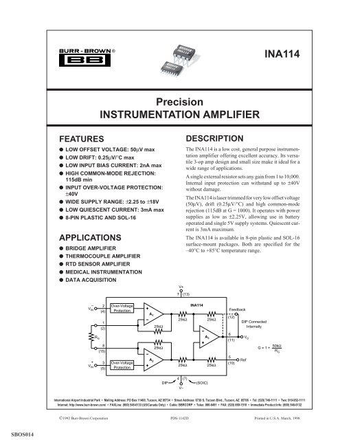
INA114 Precision INSTRUMENTATION AMPLIFIER
INA114 Precision INSTRUMENTATION AMPLIFIER
INA114 Precision INSTRUMENTATION AMPLIFIER

Create successful ePaper yourself
Turn your PDF publications into a flip-book with our unique Google optimized e-Paper software.
<strong>INA114</strong><br />
®<br />
<strong>INA114</strong><br />
<strong>INA114</strong><br />
FEATURES<br />
● LOW OFFSET VOLTAGE: 50µV max<br />
● LOW DRIFT: 0.25µV/°C max<br />
● LOW INPUT BIAS CURRENT: 2nA max<br />
● HIGH COMMON-MODE REJECTION:<br />
115dB min<br />
● INPUT OVER-VOLTAGE PROTECTION:<br />
±40V<br />
● WIDE SUPPLY RANGE: ±2.25 to ±18V<br />
● LOW QUIESCENT CURRENT: 3mA max<br />
● 8-PIN PLASTIC AND SOL-16<br />
APPLICATIONS<br />
<strong>Precision</strong><br />
<strong>INSTRUMENTATION</strong> <strong>AMPLIFIER</strong><br />
● BRIDGE <strong>AMPLIFIER</strong><br />
● THERMOCOUPLE <strong>AMPLIFIER</strong><br />
● RTD SENSOR <strong>AMPLIFIER</strong><br />
● MEDICAL <strong>INSTRUMENTATION</strong><br />
● DATA ACQUISITION<br />
DESCRIPTION<br />
The <strong>INA114</strong> is a low cost, general purpose instrumentation<br />
amplifier offering excellent accuracy. Its versatile<br />
3-op amp design and small size make it ideal for a<br />
wide range of applications.<br />
A single external resistor sets any gain from 1 to 10,000.<br />
Internal input protection can withstand up to ±40V<br />
without damage.<br />
The <strong>INA114</strong> is laser trimmed for very low offset voltage<br />
(50µV), drift (0.25µV/°C) and high common-mode<br />
rejection (115dB at G = 1000). It operates with power<br />
supplies as low as ±2.25V, allowing use in battery<br />
operated and single 5V supply systems. Quiescent current<br />
is 3mA maximum.<br />
The <strong>INA114</strong> is available in 8-pin plastic and SOL-16<br />
surface-mount packages. Both are specified for the<br />
–40°C to +85°C temperature range.<br />
V+<br />
7 (13)<br />
– 2 Over-Voltage<br />
<strong>INA114</strong><br />
V IN<br />
(4) Protection<br />
Feedback<br />
A 1<br />
(12)<br />
25kΩ<br />
25kΩ<br />
1<br />
25kΩ<br />
(2)<br />
6<br />
R G A 3 V O<br />
(11)<br />
8<br />
25kΩ<br />
(15)<br />
5<br />
A 2 Ref<br />
+ 3 Over-Voltage<br />
(10)<br />
V IN<br />
25kΩ<br />
25kΩ<br />
(5) Protection<br />
DIP Connected<br />
Internally<br />
G = 1 + 50kΩ<br />
R G<br />
DIP<br />
4<br />
V–<br />
(7)<br />
(SOIC)<br />
International Airport Industrial Park • Mailing Address: PO Box 11400, Tucson, AZ 85734 • Street Address: 6730 S. Tucson Blvd., Tucson, AZ 85706 • Tel: (520) 746-1111 • Twx: 910-952-1111<br />
Internet: http://www.burr-brown.com/ • FAXLine: (800) 548-6133 (US/Canada Only) • Cable: BBRCORP • Telex: 066-6491 • FAX: (520) 889-1510 • Immediate Product Info: (800) 548-6132<br />
1<br />
<strong>INA114</strong><br />
©1992 Burr-Brown Corporation PDS-1142D Printed in U.S.A. March, 1998<br />
®<br />
SBOS014
SPECIFICATIONS<br />
ELECTRICAL<br />
At T A = +25°C, V S = ±15V, R L = 2kΩ, unless otherwise noted.<br />
<strong>INA114</strong>BP, BU<br />
<strong>INA114</strong>AP, AU<br />
PARAMETER CONDITIONS MIN TYP MAX MIN TYP MAX UNITS<br />
INPUT<br />
Offset Voltage, RTI<br />
Initial T A = +25°C ±10 + 20/G ±50 + 100/G ±25 + 30/G ±125 + 500/G µV<br />
vs Temperature T A = T MIN to T MAX ±0.1 + 0.5/G ±0.25 + 5/G ±0.25 + 5/G ±1 + 10/G µV/°C<br />
vs Power Supply V S = ±2.25V to ±18V 0.5 + 2/G 3 + 10/G ✻ ✻ µV/V<br />
Long-Term Stability ±0.2 + 0.5/G ✻ µV/mo<br />
Impedance, Differential 10 10 || 6 ✻ Ω || pF<br />
Common-Mode 10 10 || 6 ✻ Ω || pF<br />
Input Common-Mode Range ±11 ±13.5 ✻ ✻ V<br />
Safe Input Voltage ±40 ✻ V<br />
Common-Mode Rejection V CM = ±10V, ∆R S = 1kΩ<br />
G = 1 80 96 75 90 dB<br />
G = 10 96 115 90 106 dB<br />
G = 100 110 120 106 110 dB<br />
G = 1000 115 120 106 110 dB<br />
BIAS CURRENT ±0.5 ±2 ✻ ±5 nA<br />
vs Temperature ±8 ✻ pA/°C<br />
OFFSET CURRENT ±0.5 ±2 ✻ ±5 nA<br />
vs Temperature ±8 ✻ pA/°C<br />
NOISE VOLTAGE, RTI<br />
G = 1000, R S = 0Ω<br />
f = 10Hz 15 ✻ nV/√Hz<br />
f = 100Hz 11 ✻ nV/√Hz<br />
f = 1kHz 11 ✻ nV/√Hz<br />
f B = 0.1Hz to 10Hz 0.4 ✻ µVp-p<br />
Noise Current<br />
f=10Hz 0.4 ✻ pA/√Hz<br />
f=1kHz 0.2 ✻ pA/√Hz<br />
f B = 0.1Hz to 10Hz 18 ✻ pAp-p<br />
GAIN<br />
Gain Equation 1 + (50kΩ/R G ) ✻ V/V<br />
Range of Gain 1 10000 ✻ ✻ V/V<br />
Gain Error G = 1 ±0.01 ±0.05 ✻ ✻ %<br />
G = 10 ±0.02 ±0.4 ✻ ±0.5 %<br />
G = 100 ±0.05 ±0.5 ✻ ±0.7 %<br />
G = 1000 ±0.5 ±1 ✻ ±2 %<br />
Gain vs Temperature G = 1 ±2 ±10 ✻ ±10 ppm/°C<br />
50kΩ Resistance (1) ±25 ±100 ✻ ✻ ppm/°C<br />
Nonlinearity G = 1 ±0.0001 ±0.001 ✻ ±0.002 % of FSR<br />
G = 10 ±0.0005 ±0.002 ✻ ±0.004 % of FSR<br />
G = 100 ±0.0005 ±0.002 ✻ ±0.004 % of FSR<br />
G = 1000 ±0.002 ±0.01 ✻ ±0.02 % of FSR<br />
OUTPUT<br />
Voltage I O = 5mA, T MIN to T MAX ±13.5 ±13.7 ✻ ✻ V<br />
V S = ±11.4V, R L = 2kΩ ±10 ±10.5 ✻ ✻ V<br />
V S = ±2.25V, R L = 2kΩ ±1 ±1.5 ✻ ✻ V<br />
Load Capacitance Stability 1000 ✻ pF<br />
Short Circuit Current +20/–15 ✻ mA<br />
FREQUENCY RESPONSE<br />
Bandwidth, –3dB G = 1 1 ✻ MHz<br />
G = 10 100 ✻ kHz<br />
G = 100 10 ✻ kHz<br />
G = 1000 1 ✻ kHz<br />
Slew Rate V O = ±10V, G = 10 0.3 0.6 ✻ ✻ V/µs<br />
Settling Time, 0.01% G = 1 18 ✻ µs<br />
G = 10 20 ✻ µs<br />
G = 100 120 ✻ µs<br />
G = 1000 1100 ✻ µs<br />
Overload Recovery 50% Overdrive 20 ✻ µs<br />
POWER SUPPLY<br />
Voltage Range ±2.25 ±15 ±18 ✻ ✻ ✻ V<br />
Current V IN = 0V ±2.2 ±3 ✻ ✻ mA<br />
TEMPERATURE RANGE<br />
Specification –40 85 ✻ ✻ °C<br />
Operating –40 125 ✻ ✻ °C<br />
θ JA 80 ✻ °C/W<br />
✻ Specification same as <strong>INA114</strong>BP/BU.<br />
NOTE: (1) Temperature coefficient of the “50kΩ” term in the gain equation.<br />
The information provided herein is believed to be reliable; however, BURR-BROWN assumes no responsibility for inaccuracies or omissions. BURR-BROWN assumes<br />
no responsibility for the use of this information, and all use of such information shall be entirely at the user’s own risk. Prices and specifications are subject to change<br />
without notice. No patent rights or licenses to any of the circuits described herein are implied or granted to any third party. BURR-BROWN does not authorize or warrant<br />
any BURR-BROWN product for use in life support devices and/or systems.<br />
®<br />
<strong>INA114</strong> 2
PIN CONFIGURATIONS<br />
P Package<br />
R G<br />
V – IN<br />
V + IN<br />
V–<br />
1<br />
2<br />
3<br />
4<br />
U Package<br />
Top View<br />
8-Pin DIP<br />
8<br />
7<br />
6<br />
5<br />
R G<br />
V+<br />
V O<br />
Ref<br />
SOL-16 Surface-Mount<br />
Top View<br />
ELECTROSTATIC<br />
DISCHARGE SENSITIVITY<br />
This integrated circuit can be damaged by ESD. Burr-Brown<br />
recommends that all integrated circuits be handled with appropriate<br />
precautions. Failure to observe proper handling and<br />
installation procedures can cause damage.<br />
ESD damage can range from subtle performance degradation<br />
to complete device failure. <strong>Precision</strong> integrated circuits may<br />
be more susceptible to damage because very small parametric<br />
changes could cause the device not to meet its published<br />
specifications.<br />
NC<br />
R G<br />
NC<br />
V – IN<br />
V + IN<br />
NC<br />
V–<br />
NC<br />
1<br />
2<br />
3<br />
4<br />
5<br />
6<br />
7<br />
8<br />
16<br />
15<br />
14<br />
13<br />
12<br />
11<br />
10<br />
9<br />
NC<br />
R G<br />
NC<br />
V+<br />
Feedback<br />
V O<br />
Ref<br />
NC<br />
PACKAGE/ORDERING INFORMATION<br />
PACKAGE<br />
DRAWING TEMPERATURE<br />
PRODUCT PACKAGE NUMBER (1) RANGE<br />
<strong>INA114</strong>AP 8-Pin Plastic DIP 006 –40°C to +85°C<br />
<strong>INA114</strong>BP 8-Pin Plastic DIP 006 –40°C to +85°C<br />
<strong>INA114</strong>AU SOL-16 Surface-Mount 211 –40°C to +85°C<br />
<strong>INA114</strong>BU SOL-16 Surface-Mount 211 –40°C to +85°C<br />
NOTE: (1) For detailed drawing and dimension table, please see end of data<br />
sheet, or Appendix C of Burr-Brown IC Data Book.<br />
ABSOLUTE MAXIMUM RATINGS (1)<br />
Supply Voltage .................................................................................. ±18V<br />
Input Voltage Range .......................................................................... ±40V<br />
Output Short-Circuit (to ground) .............................................. Continuous<br />
Operating Temperature ................................................. –40°C to +125°C<br />
Storage Temperature..................................................... –40°C to +125°C<br />
Junction Temperature .................................................................... +150°C<br />
Lead Temperature (soldering, 10s) ............................................... +300°C<br />
NOTE: (1) Stresses above these ratings may cause permanent damage.<br />
3<br />
<strong>INA114</strong><br />
®
TYPICAL PERFORMANCE CURVES<br />
At T A = +25°C, V S = ±15V, unless otherwise noted.<br />
Gain (V/V)<br />
1k<br />
100<br />
10<br />
1<br />
GAIN vs FREQUENCY<br />
Common-Mode Rejection (dB)<br />
140<br />
120<br />
100<br />
80<br />
60<br />
40<br />
20<br />
COMMON-MODE REJECTION vs FREQUENCY<br />
G = 100, 1k<br />
G = 10<br />
G = 1k<br />
G = 100<br />
G = 10<br />
G = 1<br />
10 100 1k 10k 100k 1M<br />
Frequency (Hz)<br />
0<br />
10 100 1k 10k 100k 1M<br />
Frequency (Hz)<br />
Common-Mode Voltage (V)<br />
15<br />
10<br />
5<br />
0<br />
–5<br />
–10<br />
INPUT COMMON-MODE VOLTAGE RANGE<br />
vs OUTPUT VOLTAGE<br />
Limited by A 1<br />
+ Output Swing<br />
–<br />
V D/2<br />
+<br />
–<br />
V D/2<br />
+<br />
V CM<br />
(Any Gain)<br />
A 3 – Output<br />
Swing Limit<br />
Limited by A 2<br />
– Output Swing<br />
–15<br />
–15 –10 –5 0 5 10 15<br />
Output Voltage (V)<br />
Limited by A 2<br />
+ Output Swing<br />
V O<br />
A 3 + Output<br />
Swing Limit<br />
Limited by A 1<br />
– Output Swing<br />
Power Supply Rejection (dB)<br />
140<br />
120<br />
100<br />
80<br />
60<br />
40<br />
20<br />
POSITIVE POWER SUPPLY REJECTION<br />
vs FREQUENCY<br />
0<br />
10 100 1k 10k 100k 1M<br />
Frequency (Hz)<br />
G = 100<br />
G = 10<br />
G = 1<br />
G = 1000<br />
Power Supply Rejection (dB)<br />
140<br />
120<br />
100<br />
80<br />
60<br />
40<br />
20<br />
NEGATIVE POWER SUPPLY REJECTION<br />
vs FREQUENCY<br />
G = 10<br />
G = 1<br />
G = 100<br />
0<br />
10 100 1k 10k 100k 1M<br />
Frequency (Hz)<br />
G = 1000<br />
Input-Referred Noise Voltage (nV/√ Hz)<br />
1k<br />
100<br />
10<br />
1<br />
INPUT-REFERRED NOISE VOLTAGE<br />
vs FREQUENCY<br />
G = 100, 1000<br />
1 10 100<br />
1k<br />
Frequency (Hz)<br />
G = 1<br />
G = 10<br />
G = 1000<br />
BW Limit<br />
10k<br />
®<br />
<strong>INA114</strong> 4
TYPICAL PERFORMANCE CURVES (CONT)<br />
At T A = +25°C, V S = ±15V, unless otherwise noted.<br />
Settling Time (µs)<br />
Input Bias and Input Offset Current (nA)<br />
SETTLING TIME vs GAIN<br />
OFFSET VOLTAGE WARM-UP vs TIME<br />
±I B<br />
I OS<br />
1200<br />
6<br />
1000<br />
4<br />
G ≥ 100<br />
800<br />
2<br />
600<br />
0.01%<br />
0<br />
400<br />
0.1%<br />
–2<br />
200<br />
–4<br />
0<br />
–6<br />
1 10<br />
100 1000<br />
0 15 30 45 60 75 90 105 120<br />
Gain (V/V)<br />
Time from Power Supply Turn-on (s)<br />
INPUT BIAS AND INPUT OFFSET CURRENT<br />
vs TEMPERATURE<br />
INPUT BIAS CURRENT<br />
vs DIFFERENTIAL INPUT VOLTAGE<br />
2<br />
3<br />
2<br />
1<br />
1<br />
0<br />
–1<br />
–2<br />
–40<br />
–15 10 35 60 85<br />
Temperature (°C)<br />
Offset Voltage Change (µV)<br />
Input Bias Current (mA)<br />
0<br />
–1<br />
–2<br />
–3<br />
–45<br />
G = 1<br />
G = 10<br />
G = 100<br />
G = 1000<br />
–30 –15 0 15 30 45<br />
Differential Overload Voltage (V)<br />
Input Bias Current (mA)<br />
3<br />
2<br />
1<br />
0<br />
–1<br />
–2<br />
–3<br />
–45<br />
Over-Voltage<br />
Protection<br />
One Input<br />
INPUT BIAS CURRENT<br />
vs COMMON-MODE INPUT VOLTAGE<br />
Normal<br />
Operation<br />
|I b1 | + |I b2 |<br />
Both Inputs<br />
One Input<br />
Over-Voltage<br />
Protection<br />
Both Inputs<br />
–30 –15 0 15 30 45<br />
Common-Mode Voltage (V)<br />
Peak-to-Peak Amplitude (V)<br />
32<br />
28<br />
24<br />
20<br />
16<br />
12<br />
8<br />
4<br />
0<br />
10<br />
MAXIMUM OUTPUT SWING vs FREQUENCY<br />
G = 1, 10<br />
G = 100<br />
G = 1000<br />
100 1k 10k 100k 1M<br />
Frequency (Hz)<br />
5<br />
<strong>INA114</strong><br />
®
TYPICAL PERFORMANCE CURVES (CONT)<br />
At T A = +25°C, V S = ±15V, unless otherwise noted.<br />
1.0<br />
SLEW RATE vs TEMPERATURE<br />
30<br />
OUTPUT CURRENT LIMIT vs TEMPERATURE<br />
Slew Rate (V/µs)<br />
0.8<br />
0.6<br />
0.4<br />
0.2<br />
Short Circuit Current (mA)<br />
25<br />
20<br />
15<br />
+|I CL |<br />
–|I CL |<br />
0<br />
–75<br />
–50 –25 0 25 50 75 100<br />
125<br />
10<br />
–40<br />
–15 10 35 60<br />
85<br />
Temperature (°C)<br />
Temperature (°C)<br />
2.8<br />
QUIESCENT CURRENT vs TEMPERATURE<br />
2.6<br />
QUIESCENT CURRENT AND POWER DISSIPATION<br />
vs POWER SUPPLY VOLTAGE<br />
120<br />
Quiescent Current (mA)<br />
2.6<br />
2.4<br />
2.2<br />
2.0<br />
Quiescent Current (mA)<br />
2.5<br />
2.4<br />
2.3<br />
2.2<br />
2.1<br />
Power Dissipation<br />
Quiescent Current<br />
100<br />
80<br />
60<br />
40<br />
20<br />
Power Dissipation (mW)<br />
1.8<br />
–75<br />
–50 –25 0 25 50 75 100<br />
Temperature (°C)<br />
125<br />
2.0<br />
0<br />
0<br />
±3 ±6 ±9 ±12 ±15 ±18<br />
Power Supply Voltage (V)<br />
16<br />
14<br />
POSITIVE SIGNAL SWING vs TEMPERATUE (R L = 2kΩ)<br />
V S = ±15V<br />
–16<br />
–14<br />
NEGATIVE SIGNAL SWING vs TEMPERATUE (R L = 2kΩ)<br />
V S = ±15V<br />
Output Voltage (V)<br />
12<br />
10<br />
8<br />
6<br />
4<br />
2<br />
V S = ±11.4V<br />
V S = ±2.25V<br />
Output Voltage (V)<br />
–12<br />
–10<br />
–8<br />
–6<br />
–4<br />
–2<br />
V S = ±11.4V<br />
V S = ±2.25V<br />
0<br />
–75<br />
–50 –25 0 25 50 75 100<br />
125<br />
0<br />
–75<br />
–50 –25 0 25 50 75 100<br />
125<br />
Temperature (°C)<br />
Temperature (°C)<br />
®<br />
<strong>INA114</strong> 6
TYPICAL PERFORMANCE CURVES (CONT)<br />
At T A = +25°C, V S = ±15V, unless otherwise noted.<br />
LARGE SIGNAL RESPONSE, G = 1 SMALL SIGNAL RESPONSE, G = 1<br />
+10V<br />
+100mV<br />
0<br />
0<br />
–10V<br />
–200mV<br />
LARGE SIGNAL RESPONSE, G = 1000 SMALL SIGNAL RESPONSE, G = 1000<br />
+10V<br />
+200mV<br />
0<br />
0<br />
–10V<br />
–200mV<br />
INPUT-REFERRED NOISE, 0.1 to 10Hz<br />
0.1µV/div<br />
1 s/div<br />
7<br />
<strong>INA114</strong><br />
®
APPLICATION INFORMATION<br />
Figure 1 shows the basic connections required for operation<br />
of the <strong>INA114</strong>. Applications with noisy or high impedance<br />
power supplies may require decoupling capacitors close to<br />
the device pins as shown.<br />
The output is referred to the output reference (Ref) terminal<br />
which is normally grounded. This must be a low-impedance<br />
connection to assure good common-mode rejection. A resistance<br />
of 5Ω in series with the Ref pin will cause a typical<br />
device to degrade to approximately 80dB CMR (G = 1).<br />
SETTING THE GAIN<br />
Gain of the <strong>INA114</strong> is set by connecting a single external<br />
resistor, R G :<br />
G = 1 +<br />
50 kΩ<br />
R G<br />
(1)<br />
Commonly used gains and resistor values are shown in<br />
Figure 1.<br />
The 50kΩ term in equation (1) comes from the sum of the<br />
two internal feedback resistors. These are on-chip metal film<br />
resistors which are laser trimmed to accurate absolute val-<br />
ues. The accuracy and temperature coefficient of these<br />
resistors are included in the gain accuracy and drift specifications<br />
of the <strong>INA114</strong>.<br />
The stability and temperature drift of the external gain<br />
setting resistor, R G , also affects gain. R G ’s contribution to<br />
gain accuracy and drift can be directly inferred from the gain<br />
equation (1). Low resistor values required for high gain can<br />
make wiring resistance important. Sockets add to the wiring<br />
resistance which will contribute additional gain error (possibly<br />
an unstable gain error) in gains of approximately 100 or<br />
greater.<br />
NOISE PERFORMANCE<br />
The <strong>INA114</strong> provides very low noise in most applications.<br />
For differential source impedances less than 1kΩ, the INA103<br />
may provide lower noise. For source impedances greater<br />
than 50kΩ, the INA111 FET-input instrumentation amplifier<br />
may provide lower noise.<br />
Low frequency noise of the <strong>INA114</strong> is approximately<br />
0.4µVp-p measured from 0.1 to 10Hz. This is approximately<br />
one-tenth the noise of “low noise” chopper-stabilized amplifiers.<br />
V+<br />
0.1µF<br />
Pin numbers are<br />
for DIP packages.<br />
7<br />
– 2 Over-Voltage<br />
<strong>INA114</strong><br />
V IN<br />
Protection<br />
A 1<br />
25kΩ<br />
25kΩ<br />
1<br />
25kΩ<br />
6<br />
R G A 3<br />
8<br />
25kΩ<br />
5<br />
A<br />
+<br />
2<br />
3 Over-Voltage<br />
V IN<br />
25kΩ<br />
25kΩ<br />
Protection<br />
+ –<br />
V O = G • (V IN – V IN )<br />
G = 1 + 50kΩ<br />
R G<br />
Load<br />
+<br />
V O<br />
–<br />
4<br />
0.1µF<br />
DESIRED R G<br />
NEAREST 1% R G<br />
GAIN (Ω) (Ω)<br />
1 No Connection No Connection<br />
2 50.00k 49.9k<br />
5 12.50k 12.4k<br />
10 5.556k 5.62k<br />
20 2.632k 2.61k<br />
50 1.02k 1.02k<br />
100 505.1 511<br />
200 251.3 249<br />
500 100.2 100<br />
1000 50.05 49.9<br />
2000 25.01 24.9<br />
5000 10.00 10<br />
10000 5.001 4.99<br />
V–<br />
Also drawn in simplified form:<br />
V<br />
– IN<br />
R G <strong>INA114</strong> V O<br />
V<br />
+<br />
Ref<br />
IN<br />
FIGURE 1. Basic Connections.<br />
®<br />
<strong>INA114</strong> 8
OFFSET TRIMMING<br />
The <strong>INA114</strong> is laser trimmed for very low offset voltage and<br />
drift. Most applications require no external offset adjustment.<br />
Figure 2 shows an optional circuit for trimming the<br />
output offset voltage. The voltage applied to Ref terminal is<br />
summed at the output. Low impedance must be maintained<br />
at this node to assure good common-mode rejection. This is<br />
achieved by buffering trim voltage with an op amp as<br />
shown.<br />
Microphone,<br />
Hydrophone<br />
etc.<br />
47kΩ<br />
47kΩ<br />
<strong>INA114</strong><br />
–<br />
V IN<br />
R G<br />
+<br />
V IN<br />
<strong>INA114</strong><br />
Ref<br />
V O<br />
V+<br />
100µA<br />
1/2 REF200<br />
Thermocouple<br />
10kΩ<br />
<strong>INA114</strong><br />
OPA177<br />
±10mV<br />
Adjustment Range<br />
10kΩ<br />
100Ω<br />
100Ω<br />
<strong>INA114</strong><br />
100µA<br />
1/2 REF200<br />
FIGURE 2. Optional Trimming of Output Offset Voltage.<br />
INPUT BIAS CURRENT RETURN PATH<br />
The input impedance of the <strong>INA114</strong> is extremely high—<br />
approximately 10 10 Ω. However, a path must be provided for<br />
the input bias current of both inputs. This input bias current<br />
is typically less than ±1nA (it can be either polarity due to<br />
cancellation circuitry). High input impedance means that<br />
this input bias current changes very little with varying input<br />
voltage.<br />
Input circuitry must provide a path for this input bias current<br />
if the <strong>INA114</strong> is to operate properly. Figure 3 shows various<br />
provisions for an input bias current path. Without a bias<br />
current return path, the inputs will float to a potential which<br />
exceeds the common-mode range of the <strong>INA114</strong> and the<br />
input amplifiers will saturate. If the differential source resistance<br />
is low, bias current return path can be connected to one<br />
input (see thermocouple example in Figure 3). With higher<br />
source impedance, using two resistors provides a balanced<br />
input with possible advantages of lower input offset voltage<br />
due to bias current and better common-mode rejection.<br />
INPUT COMMON-MODE RANGE<br />
The linear common-mode range of the input op amps of the<br />
<strong>INA114</strong> is approximately ±13.75V (or 1.25V from the<br />
power supplies). As the output voltage increases, however,<br />
the linear input range will be limited by the output voltage<br />
swing of the input amplifiers, A 1 and A 2 . The commonmode<br />
range is related to the output voltage of the complete<br />
amplifier—see performance curve “Input Common-Mode<br />
Range vs Output Voltage.”<br />
V–<br />
Center-tap provides<br />
bias current return.<br />
FIGURE 3. Providing an Input Common-Mode Current Path.<br />
A combination of common-mode and differential input<br />
signals can cause the output of A 1 or A 2 to saturate. Figure<br />
4 shows the output voltage swing of A 1 and A 2 expressed in<br />
terms of a common-mode and differential input voltages.<br />
Output swing capability of these internal amplifiers is the<br />
same as the output amplifier, A 3 . For applications where<br />
input common-mode range must be maximized, limit the<br />
output voltage swing by connecting the <strong>INA114</strong> in a lower<br />
gain (see performance curve “Input Common-Mode Voltage<br />
Range vs Output Voltage”). If necessary, add gain after the<br />
<strong>INA114</strong> to increase the voltage swing.<br />
Input-overload often produces an output voltage that appears<br />
normal. For example, an input voltage of +20V on one input<br />
and +40V on the other input will obviously exceed the linear<br />
common-mode range of both input amplifiers. Since both<br />
input amplifiers are saturated to nearly the same output<br />
voltage limit, the difference voltage measured by the output<br />
amplifier will be near zero. The output of the <strong>INA114</strong> will<br />
be near 0V even though both inputs are overloaded.<br />
INPUT PROTECTION<br />
The inputs of the <strong>INA114</strong> are individually protected for<br />
voltages up to ±40V. For example, a condition of –40V on<br />
one input and +40V on the other input will not cause<br />
damage. Internal circuitry on each input provides low series<br />
impedance under normal signal conditions. To provide<br />
equivalent protection, series input resistors would contribute<br />
excessive noise. If the input is overloaded, the protection<br />
circuitry limits the input current to a safe value (approximately<br />
1.5mA). The typical performance curve “Input Bias<br />
Current vs Common-Mode Input Voltage” shows this input<br />
9<br />
<strong>INA114</strong><br />
®
current limit behavior. The inputs are protected even if no<br />
power supply voltage is present.<br />
OUTPUT VOLTAGE SENSE (SOL-16 package only)<br />
The surface-mount version of the <strong>INA114</strong> has a separate<br />
output sense feedback connection (pin 12). Pin 12 must be<br />
connected to the output terminal (pin 11) for proper operation.<br />
(This connection is made internally on the DIP version<br />
of the <strong>INA114</strong>.)<br />
The output sense connection can be used to sense the output<br />
voltage directly at the load for best accuracy. Figure 5 shows<br />
how to drive a load through series interconnection resistance.<br />
Remotely located feedback paths may cause instability.<br />
This can be generally be eliminated with a high<br />
frequency feedback path through C 1 . Heavy loads or long<br />
lines can be driven by connecting a buffer inside the feedback<br />
path (Figure 6).<br />
V D2<br />
V+<br />
V CM – G • V D<br />
2<br />
<strong>INA114</strong><br />
Over-Voltage<br />
Protection<br />
A 1<br />
25kΩ<br />
25kΩ<br />
25kΩ<br />
R G<br />
G = 1 + 50kΩ<br />
R G<br />
V O = G • V D<br />
A 3<br />
25kΩ<br />
V D2<br />
25kΩ<br />
V CM<br />
Over-Voltage<br />
Protection<br />
A 2<br />
25kΩ<br />
V CM + G • V D<br />
2<br />
V–<br />
FIGURE 4. Voltage Swing of A 1 and A 2 .<br />
Surface-mount package<br />
version only.<br />
Surface-mount package<br />
version only.<br />
V IN<br />
–<br />
V IN<br />
+<br />
R G<br />
<strong>INA114</strong><br />
Output<br />
Sense<br />
Ref<br />
C 1<br />
1000pF<br />
Load<br />
V IN<br />
–<br />
V IN<br />
+<br />
R G<br />
Output<br />
Sense<br />
<strong>INA114</strong><br />
Ref<br />
180Ω<br />
OPA633<br />
R L<br />
I L : ±100mA<br />
Equal resistance here preserves<br />
good common-mode rejection.<br />
FIGURE 5. Remote Load and Ground Sensing.<br />
FIGURE 6. Buffered Output for Heavy Loads.<br />
V IN<br />
–<br />
V IN<br />
+<br />
Shield is driven at the<br />
common-mode potential.<br />
100Ω<br />
OPA602<br />
22.1kΩ<br />
22.1kΩ<br />
511Ω<br />
For G = 100<br />
R G = 511Ω // 2(22.1kΩ)<br />
effective R G = 505Ω<br />
<strong>INA114</strong><br />
Ref<br />
V O<br />
FIGURE 7. Shield Driver Circuit.<br />
®<br />
<strong>INA114</strong> 10
V+ V+<br />
Equal line resistance here creates<br />
a small common-mode voltage<br />
which is rejected by <strong>INA114</strong>.<br />
1<br />
REF200<br />
100µA<br />
RTD<br />
R G<br />
<strong>INA114</strong><br />
V O<br />
2<br />
Ref<br />
3<br />
R Z<br />
Resistance in this line causes<br />
a small common-mode voltage<br />
which is rejected by <strong>INA114</strong>.<br />
V O = 0V at R RTD = R Z<br />
FIGURE 8. RTD Temperature Measurement Circuit.<br />
V+<br />
2<br />
10.0V<br />
6<br />
REF102<br />
R1<br />
27k Ω<br />
R4<br />
80.6k Ω<br />
4<br />
K<br />
1N4148<br />
(1)<br />
Cu<br />
Cu<br />
R2<br />
5.23k Ω<br />
(2)<br />
R7<br />
1MΩ<br />
<strong>INA114</strong><br />
Ref<br />
V O<br />
R3<br />
100Ω<br />
R5<br />
50Ω<br />
R6<br />
100Ω<br />
Zero Adj<br />
SEEBECK<br />
ISA COEFFICIENT R 2 R 4<br />
TYPE MATERIAL (µV/°C) (R 3 = 100Ω) (R 5 + R 6 = 100Ω)<br />
E Chromel 58.5 3.48kΩ 56.2kΩ<br />
Constantan<br />
J Iron 50.2 4.12kΩ 64.9kΩ<br />
Constantan<br />
K Chromel 39.4 5.23kΩ 80.6kΩ<br />
Alumel<br />
T Copper 38.0 5.49kΩ 84.5kΩ<br />
Constantan<br />
NOTES: (1) –2.1mV/°C at 200µA. (2) R 7 provides down-scale burn-out indication.<br />
FIGURE 9. Thermocouple Amplifier With Cold Junction Compensation.<br />
11<br />
<strong>INA114</strong><br />
®
2.8kΩ<br />
RA<br />
LA<br />
R G/2<br />
<strong>INA114</strong><br />
V O<br />
2.8kΩ<br />
Ref<br />
G = 10<br />
RL<br />
390kΩ<br />
390kΩ<br />
1/2<br />
OPA2604<br />
10kΩ<br />
1/2<br />
OPA2604<br />
FIGURE 10. ECG Amplifier With Right-Leg Drive.<br />
+10V<br />
–<br />
V IN<br />
+<br />
R G<br />
<strong>INA114</strong><br />
Ref R 1<br />
V O<br />
Bridge<br />
G = 500<br />
C 1<br />
0.1µF<br />
1MΩ<br />
R G<br />
100Ω<br />
<strong>INA114</strong><br />
Ref<br />
V O<br />
OPA602<br />
1<br />
f –3dB =<br />
2πR 1 C 1<br />
= 1.59Hz<br />
FIGURE 11. Bridge Transducer Amplifier.<br />
FIGURE 12. AC-Coupled Instrumentation Amplifier.<br />
–<br />
V IN<br />
+<br />
R G<br />
<strong>INA114</strong><br />
Ref<br />
R 1<br />
I B<br />
I O =<br />
V IN<br />
R<br />
• G<br />
A 1<br />
Load<br />
I O<br />
A 1<br />
OPA177<br />
OPA602<br />
OPA128<br />
I B<br />
Error<br />
±1.5nA<br />
1pA<br />
75fA<br />
FIGURE 13. Differential Voltage-to-Current Converter.<br />
®<br />
<strong>INA114</strong> 12
IMPORTANT NOTICE<br />
Texas Instruments and its subsidiaries (TI) reserve the right to make changes to their products or to discontinue<br />
any product or service without notice, and advise customers to obtain the latest version of relevant information<br />
to verify, before placing orders, that information being relied on is current and complete. All products are sold<br />
subject to the terms and conditions of sale supplied at the time of order acknowledgment, including those<br />
pertaining to warranty, patent infringement, and limitation of liability.<br />
TI warrants performance of its semiconductor products to the specifications applicable at the time of sale in<br />
accordance with TI’s standard warranty. Testing and other quality control techniques are utilized to the extent<br />
TI deems necessary to support this warranty. Specific testing of all parameters of each device is not necessarily<br />
performed, except those mandated by government requirements.<br />
Customers are responsible for their applications using TI components.<br />
In order to minimize risks associated with the customer’s applications, adequate design and operating<br />
safeguards must be provided by the customer to minimize inherent or procedural hazards.<br />
TI assumes no liability for applications assistance or customer product design. TI does not warrant or represent<br />
that any license, either express or implied, is granted under any patent right, copyright, mask work right, or other<br />
intellectual property right of TI covering or relating to any combination, machine, or process in which such<br />
semiconductor products or services might be or are used. TI’s publication of information regarding any third<br />
party’s products or services does not constitute TI’s approval, warranty or endorsement thereof.<br />
Copyright © 2000, Texas Instruments Incorporated