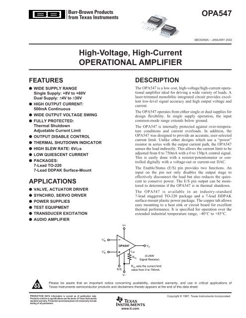
OPA547: High-Voltage,High-Current Operational Amplifier (Rev. A)
OPA547: High-Voltage,High-Current Operational Amplifier (Rev. A)
OPA547: High-Voltage,High-Current Operational Amplifier (Rev. A)

You also want an ePaper? Increase the reach of your titles
YUMPU automatically turns print PDFs into web optimized ePapers that Google loves.
<strong>OPA547</strong><br />
<strong>OPA547</strong><br />
<strong>OPA547</strong><br />
SBOS056A – JANUARY 2002<br />
<strong>High</strong>-<strong>Voltage</strong>, <strong>High</strong>-<strong>Current</strong><br />
OPERATIONAL AMPLIFIER<br />
FEATURES<br />
● WIDE SUPPLY RANGE<br />
Single Supply: +8V to +60V<br />
Dual Supply: ±4V to ±30V<br />
● HIGH OUTPUT CURRENT:<br />
500mA Continuous<br />
● WIDE OUTPUT VOLTAGE SWING<br />
● FULLY PROTECTED:<br />
Thermal Shutdown<br />
Adjustable <strong>Current</strong> Limit<br />
● OUTPUT DISABLE CONTROL<br />
● THERMAL SHUTDOWN INDICATOR<br />
● HIGH SLEW RATE: 6V/µs<br />
● LOW QUIESCENT CURRENT<br />
● PACKAGES:<br />
7-Lead TO-220<br />
7-Lead DDPAK Surface-Mount<br />
APPLICATIONS<br />
● VALVE, ACTUATOR DRIVER<br />
● SYNCHRO, SERVO DRIVER<br />
● POWER SUPPLIES<br />
● TEST EQUIPMENT<br />
● TRANSDUCER EXCITATION<br />
● AUDIO AMPLIFIER<br />
V+<br />
DESCRIPTION<br />
The <strong>OPA547</strong> is a low cost, high-voltage/high-current operational<br />
amplifier ideal for driving a wide variety of loads. A<br />
laser-trimmed monolithic integrated circuit provides excellent<br />
low-level signal accuracy and high output voltage and<br />
current.<br />
The <strong>OPA547</strong> operates from either single or dual supplies for<br />
design flexibility. In single supply operation, the input<br />
common-mode range extends below ground.<br />
The <strong>OPA547</strong> is internally protected against over-temperature<br />
conditions and current overloads. In addition, the<br />
<strong>OPA547</strong> was designed to provide an accurate, user-selected<br />
current limit. Unlike other designs which use a “power”<br />
resistor in series with the output current path, the <strong>OPA547</strong><br />
senses the load indirectly. This allows the current limit to be<br />
adjusted from 0 to 750mA with a 0 to 150µA control signal.<br />
This is easily done with a resistor/potentiometer or controlled<br />
digitally with a voltage-out or current-out DAC.<br />
The Enable/Status (E/S) pin provides two functions. An<br />
input on the pin not only disables the output stage to<br />
effectively disconnect the load but also reduces the quiescent<br />
to conserve power. The E/S pin output can be monitored<br />
to determine if the <strong>OPA547</strong> is in thermal shutdown.<br />
The <strong>OPA547</strong> is available in an industry-standard<br />
7-lead staggered TO-220 package and a 7-lead DDPAK<br />
surface-mount plastic power package. The copper tab allows<br />
easy mounting to a heat sink or circuit board for excellent<br />
thermal performance. It is specified for operation over the<br />
extended industrial temperature range, –40°C to +85°C.<br />
V IN<br />
–<br />
<strong>OPA547</strong><br />
V O<br />
V IN<br />
+<br />
I LIM<br />
R CL<br />
(0.25W<br />
Signal Resistor)<br />
E/S<br />
R CL sets the current limit<br />
value from 0 to 750mA.<br />
V–<br />
Please be aware that an important notice concerning availability, standard warranty, and use in critical applications of<br />
Texas Instruments semiconductor products and disclaimers thereto appears at the end of this data sheet.<br />
PRODUCTION DATA information is current as of publication date.<br />
Products conform to specifications per the terms of Texas Instruments<br />
standard warranty. Production processing does not necessarily include<br />
testing of all parameters.<br />
Copyright © 1997, Texas Instruments Incorporated<br />
www.ti.com
ABSOLUTE MAXIMUM RATINGS (1)<br />
Output <strong>Current</strong> ................................................................. See SOA Curve<br />
Supply <strong>Voltage</strong>, V+ to V– ................................................................... 60V<br />
Input <strong>Voltage</strong> ....................................................... (V–)–0.5V to (V+)+0.5V<br />
Input Shutdown <strong>Voltage</strong> ........................................................................ V+<br />
Operating Temperature .................................................. –40°C to +125°C<br />
Storage Temperature ..................................................... –55°C to +125°C<br />
Junction Temperature ...................................................................... 150°C<br />
Lead Temperature (soldering 10s) (2) .............................................. 300°C<br />
NOTE: (1) Stresses above these ratings may cause permanent damage. (2)<br />
Vapor-phase or IR reflow techniques are recommended for soldering the<br />
<strong>OPA547</strong>F surface mount package. Wave soldering is not recommended due to<br />
excessive thermal shock and “shadowing” of nearby devices.<br />
ELECTROSTATIC<br />
DISCHARGE SENSITIVITY<br />
This integrated circuit can be damaged by ESD. Texas Instruments<br />
recommends that all integrated circuits be handled with<br />
appropriate precautions. Failure to observe proper handling<br />
and installation procedures can cause damage.<br />
ESD damage can range from subtle performance degradation<br />
to complete device failure. Precision integrated circuits may<br />
be more susceptible to damage because very small parametric<br />
changes could cause the device not to meet its published<br />
specifications.<br />
PACKAGE/ORDERING INFORMATION<br />
SPECIFIED<br />
PACKAGE TEMPERATURE PACKAGE ORDERING TRANSPORT<br />
PRODUCT PACKAGE-LEAD DESIGNATOR (1) RANGE MARKING NUMBER MEDIA, QUANTITY<br />
<strong>OPA547</strong>T TO-220-7 KV –40°C to +85°C <strong>OPA547</strong>T <strong>OPA547</strong>T Tubes, 49<br />
<strong>OPA547</strong>F DDPAK-7 KTW –40°C to +85°C <strong>OPA547</strong>F <strong>OPA547</strong>F Tubes, 49<br />
" " " " <strong>OPA547</strong>F <strong>OPA547</strong>F/500 Tape and Reel, 500<br />
NOTES: (1) For the most current specifications and package information, refer to our web site at www.ti.com.<br />
PIN CONFIGURATIONS<br />
Top Front View<br />
7-Lead<br />
Stagger-Formed<br />
TO-220<br />
7-Lead<br />
DDPAK<br />
Surface-Mount<br />
1 2 3 4 5 6<br />
7<br />
1 2 3 4 5 6<br />
7<br />
+<br />
V IN I LIM V+ E/S<br />
–<br />
V IN V– V O<br />
+<br />
V IN I LIM V+ E/S<br />
–<br />
V IN V– V O<br />
NOTE: Tabs are electrically connected to V– supply.<br />
2<br />
www.ti.com<br />
<strong>OPA547</strong><br />
SBOS056A
ELECTRICAL CHARACTERISTICS<br />
At T CASE = +25°C, V S = ±30V and E/S pin open, unless otherwise noted.<br />
<strong>OPA547</strong>T, F<br />
PARAMETER CONDITION MIN TYP MAX UNITS<br />
OFFSET VOLTAGE<br />
Input Offset <strong>Voltage</strong> V CM = 0, I O = 0 ±1 ±5 mV<br />
vs Temperature T A = –40°C to +85°C ±25 µV/°C<br />
vs Power Supply V S = ±4V to ±30V 10 100 µV/V<br />
INPUT BIAS CURRENT (1)<br />
Input Bias <strong>Current</strong> (2) V CM = 0V –100 –500 nA<br />
vs Temperature ±0.5 nA/°C<br />
Input Offset <strong>Current</strong> V CM = 0V ±5 ±50 nA<br />
NOISE<br />
Input <strong>Voltage</strong> Noise Density, f = 1kHz 90 nV/√Hz<br />
<strong>Current</strong> Noise Density, f = 1kHz 200 fA/√Hz<br />
INPUT VOLTAGE RANGE<br />
Common-Mode <strong>Voltage</strong> Range: Positive Linear Operation (V+) –3 (V+) –2.3 V<br />
Negative Linear Operation (V–) –0.1 (V–) –0.2 V<br />
Common-Mode Rejection V CM = (V–) –0.1V to (V+) –3V 80 95 dB<br />
INPUT IMPEDANCE<br />
Differential 10 7 || 6 Ω || pF<br />
Common-Mode 10 9 || 4 Ω || pF<br />
OPEN-LOOP GAIN<br />
Open-Loop <strong>Voltage</strong> Gain, f = 10Hz V O = ±25V, R L = 1kΩ 100 115 dB<br />
V O = ±25V, R L = 50Ω 110 dB<br />
FREQUENCY RESPONSE<br />
Gain-Bandwidth Product R L = 50Ω 1 MHz<br />
Slew Rate G = 1, 50Vp-p, R L = 50Ω 6 V/µs<br />
Full Power Bandwidth See Typical Curve kHz<br />
Settling Time: ±0.1% G = –10, 50V Step 18 µs<br />
Total Harmonic Distortion + Noise, f = 1kHz R L = 50Ω, G = +3V, 1W Power 0.004 (3) %<br />
OUTPUT<br />
<strong>Voltage</strong> Output, Positive I O = 0.5A (V+) –2.2 (V+) –1.9 V<br />
Negative I O = –0.5A (V–) +1.6 (V–) +1.3 V<br />
Positive I O = 0.1A (V+) –1.8 (V+) –1.5 V<br />
Negative I O = –0.1A (V–) +1.2 (V–) +0.8 V<br />
Maximum Continuous <strong>Current</strong> Output: dc ±500 mA<br />
ac 500 mArms<br />
Leakage <strong>Current</strong>, Output Disabled, dc<br />
See Typical Curve<br />
Output <strong>Current</strong> Limit<br />
<strong>Current</strong> Limit Range 0 to ±750 mA<br />
<strong>Current</strong> Limit Equation I LIM = (5000)(4.75)/(31600Ω + R CL ) A<br />
<strong>Current</strong> Limit Tolerance (1) R CL = 31.6kΩ (I LIM = ±375mA), ±10 ±30 mA<br />
R L = 50Ω<br />
Capacitive Load Drive See Typical Curve (4)<br />
OUTPUT ENABLE /STATUS (E/S) PIN<br />
Shutdown Input Mode<br />
V E/S <strong>High</strong> (output enabled) E/S Pin Open or Forced <strong>High</strong> (V–) +2.4 V<br />
V E/S Low (output disabled) E/S Pin Forced Low (V–) +0.8 V<br />
I E/S <strong>High</strong> (output enabled) E/S Pin <strong>High</strong> –60 µA<br />
I E/S Low (output disabled) E/S Pin Low –65 µA<br />
Output Disable Time 1 µs<br />
Output Enable Time 3 ms<br />
Thermal Shutdown Status Output<br />
Normal Operation Sourcing 20µA (V–) +2.4 (V–) +3.5 V<br />
Thermally Shutdown Sinking 5µA, T J > 160°C (V–) +0.35 (V–) +0.8 V<br />
Junction Temperature, Shutdown +160 °C<br />
Reset from Shutdown +140 °C<br />
POWER SUPPLY<br />
Specified <strong>Voltage</strong> ±30 V<br />
Operating <strong>Voltage</strong> Range ±4 ±30 V<br />
Quiescent <strong>Current</strong> I LIM Connected to V–, I O = 0 ±10 ±15 mA<br />
Quiescent <strong>Current</strong>, Shutdown Mode I LIM Connected to V– ±4 mA<br />
TEMPERATURE RANGE<br />
Specified Range –40 +85 °C<br />
Operating Range –40 +125 °C<br />
Storage Range –55 +125 °C<br />
Thermal Resistance, θ JC<br />
7-Lead DDPAK, 7-Lead TO-220 f > 50Hz 2 °C/W<br />
7-Lead DDPAK, 7-Lead TO-220 dc 3 °C/W<br />
Thermal Resistance, θ JA<br />
7-Lead DDPAK, 7-Lead TO-220 No Heat Sink 65 °C/W<br />
NOTES: (1) <strong>High</strong>-speed test at T J = +25°C. (2) Positive conventional current flows into the input terminals. (3) See “Total Harmonic Distortion+Noise” in the Typical<br />
Characteristics section for additional power levels. (4) See “Small-Signal Overshoot vs Load Capacitance” in the Typical Characteristics section.<br />
<strong>OPA547</strong> 3<br />
SBOS056A<br />
www.ti.com
TYPICAL CHARACTERISTICS<br />
At T CASE = +25°C, V S = ±30V and E/S pin open, unless otherwise noted.<br />
Gain (dB)<br />
120<br />
100<br />
80<br />
60<br />
40<br />
20<br />
φ<br />
OPEN-LOOP GAIN AND PHASE<br />
vs FREQUENCY<br />
G<br />
R L = 50Ω<br />
0<br />
–45<br />
–90<br />
–135<br />
Phase (°)<br />
Input Bias <strong>Current</strong> (nA)<br />
–160<br />
–140<br />
–120<br />
–100<br />
–80<br />
–60<br />
–40<br />
INPUT BIAS CURRENT vs TEMPERATURE<br />
I B<br />
V S = ±5V<br />
V S = ±30V<br />
0<br />
–180<br />
–20<br />
–20<br />
1 10 100 1k 10k 100k 1M 10M<br />
Frequency (Hz)<br />
0<br />
–75 –50 –25 0 25 50 75 100 125 150<br />
Temperature (°C)<br />
<strong>Current</strong> Limit (mA)<br />
±600<br />
±500<br />
±400<br />
±300<br />
±200<br />
CURRENT LIMIT vs TEMPERATURE<br />
R CL = 15.9kΩ<br />
R CL = 31.6kΩ<br />
R CL = 63.4kΩ<br />
<strong>Current</strong> Limit (mA)<br />
±600<br />
±550<br />
±500<br />
±450<br />
+400<br />
±350<br />
±300<br />
±250<br />
CURRENT LIMIT vs SUPPLY VOLTAGE<br />
+I LIM<br />
–I LIM<br />
R CL = 15.9kΩ<br />
R CL = 31.6kΩ<br />
R CL = 63.4kΩ<br />
±100<br />
–75 –50 –25 0 25 50 75 100 125 150<br />
Temperature (°C)<br />
±200<br />
0 ±5 ±10 ±15 ±20 ±25 ±30<br />
Supply <strong>Voltage</strong> (V)<br />
400<br />
VOLTAGE NOISE DENSITY vs FREQUENCY<br />
±12<br />
QUIESCENT CURRENT vs TEMPERATURE<br />
V S = ±30V<br />
<strong>Voltage</strong> Noise (nV/√Hz)<br />
300<br />
200<br />
100<br />
0<br />
1 10 100 1k 10k 100k 1M<br />
Frequency (Hz)<br />
Quiescent <strong>Current</strong> (mA)<br />
I Q<br />
±10<br />
±8<br />
V S = ±5V<br />
±6<br />
V S = ±30V<br />
I Q Shutdown<br />
±4<br />
V S = ±5V<br />
±2<br />
–75 –50 –25 0 25 50 75 100 125 150<br />
Temperature (°C)<br />
4<br />
www.ti.com<br />
<strong>OPA547</strong><br />
SBOS056A
TYPICAL CHARACTERISTICS (Cont.)<br />
At T CASE = +25°C, V S = ±30V and E/S pin open, unless otherwise noted.<br />
100<br />
COMMON-MODE REJECTION vs FREQUENCY<br />
120<br />
POWER SUPPLY REJECTION<br />
vs FREQUENCY<br />
Common-Mode Rejection (dB)<br />
90<br />
80<br />
70<br />
60<br />
50<br />
40<br />
30<br />
Power Supply Rejection (dB)<br />
100<br />
80<br />
60<br />
40<br />
20<br />
–PSRR<br />
+PSRR<br />
20<br />
10 100 1k 10k 100k 1M<br />
Frequency (Hz)<br />
0<br />
1 10 100 1k 10k 100k 1M<br />
Frequency (Hz)<br />
50<br />
SMALL-SIGNAL OVERSHOOT<br />
vs LOAD CAPACITANCE<br />
105<br />
OPEN-LOOP GAIN, COMMON-MODE REJECTION,<br />
AND POWER SUPPLY REJECTION vs TEMPERATURE<br />
120<br />
40<br />
100<br />
A OL<br />
115<br />
Overshoot (%)<br />
3<br />
20<br />
G = +1<br />
G = –1<br />
CMRR (dB)<br />
95<br />
CMRR<br />
PSRR<br />
100<br />
PSRR, A OL (dB)<br />
10<br />
90<br />
95<br />
0<br />
0 2k 4k 6k 8k 10k 12k 14k 16k 18k 20k<br />
Load Capacitance (pF)<br />
85<br />
90<br />
–75 –50 –25 0 25 50 75 100 125 150<br />
Temperature (°C)<br />
Gain-Bandwidth Product (MHz)<br />
1.25<br />
1<br />
0.75<br />
0.5<br />
0.25<br />
SR–<br />
GAIN-BANDWIDTH PRODUCT AND<br />
SLEW RATE vs TEMPERATURE<br />
GBW<br />
SR+<br />
7.5<br />
7<br />
6.5<br />
6<br />
5.5<br />
Slew Rate (V/µs)<br />
THD+N (%)<br />
0.1<br />
0.01<br />
0.001<br />
R L = 50Ω<br />
G = +3<br />
TOTAL HARMONIC DISTORTION+NOISE<br />
vs FREQUENCY<br />
0.1W<br />
1W<br />
6.25W<br />
0<br />
5<br />
–75 –50 –25 0 25 50 75 100 125 150<br />
Temperature (°C)<br />
0.0001<br />
20 100 1k 10k 20k<br />
Frequency (Hz)<br />
<strong>OPA547</strong> 5<br />
SBOS056A<br />
www.ti.com
TYPICAL CHARACTERISTICS (Cont.)<br />
At T CASE = +25°C, V S = ±30V and E/S pin open, unless otherwise noted.<br />
3<br />
OUTPUT VOLTAGE SWING vs OUTPUT CURRENT<br />
2.5<br />
OUTPUT VOLTAGE SWING vs TEMPERATURE<br />
⏐V SUPPLY ⏐– ⏐V OUT ⏐ (V)<br />
2.5<br />
2<br />
1.5<br />
1<br />
0.5<br />
(V+) –V O<br />
⏐(V–) –V O ⏐<br />
⏐V SUPPLY ⏐ – ⏐V OUT ⏐ (V)<br />
2<br />
1.5<br />
1<br />
0.5<br />
I O = +100mA I O = +500mA<br />
I O = –500mA<br />
I O = –100mA<br />
0<br />
0 100 200 300 400 500 600<br />
Output <strong>Current</strong> (mA)<br />
0<br />
–75 –50 –25 0 25 50 75 100 125 150<br />
Temperature (°C)<br />
Output <strong>Voltage</strong> (Vp)<br />
30<br />
25<br />
20<br />
15<br />
10<br />
5<br />
MAXIMUM OUTPUT VOLTAGE SWING<br />
vs FREQUENCY<br />
Maximum Output<br />
<strong>Voltage</strong> Without<br />
Slew Rate Induced<br />
Distortion<br />
0<br />
1k 10k 100k 1M<br />
Frequency (Hz)<br />
Leakage <strong>Current</strong> (mA)<br />
1<br />
0.5<br />
0<br />
–0.5<br />
OUTPUT LEAKAGE CURRENT<br />
vs APPLIED OUTPUT VOLTAGE<br />
R CL<br />
= 31.6kΩ<br />
–1<br />
–40 –30 –20 –10 0 10 20 30<br />
Output <strong>Voltage</strong> (V)<br />
R CL<br />
= ∞<br />
R CL<br />
= 0<br />
R L<br />
= 10Ω<br />
V S<br />
= ±30V<br />
Output Disabled<br />
V E/S < (V–) + 0.8V<br />
Percent of <strong>Amplifier</strong>s (%)<br />
20<br />
18<br />
16<br />
14<br />
12<br />
10<br />
8<br />
6<br />
4<br />
Typical production<br />
distribution of<br />
packaged units.<br />
OFFSET VOLTAGE<br />
PRODUCTION DISTRIBUTION<br />
Percent of <strong>Amplifier</strong>s (%)<br />
25<br />
20<br />
15<br />
10<br />
5<br />
OFFSET VOLTAGE DRIFT<br />
PRODUCTION DISTRIBUTION<br />
Typical production<br />
distribution of<br />
packaged units.<br />
2<br />
0<br />
–5 –4 –3 –2 –1 0 1 2 3 4 5<br />
Offset <strong>Voltage</strong> (mV)<br />
0<br />
0 5 10 15 20 25 30 35 40 45 50 55 60 65 70<br />
Offset <strong>Voltage</strong> Drift (µV/°C)<br />
6<br />
www.ti.com<br />
<strong>OPA547</strong><br />
SBOS056A
TYPICAL CHARACTERISTICS (Cont.)<br />
At T CASE = +25°C, V S = ±35V and E/S pin open, unless otherwise noted.<br />
SMALL SIGNAL STEP RESPONSE<br />
G = 1, C L = 1000pF<br />
SMALL SIGNAL STEP RESPONSE<br />
G = 3, C L = 1000pF<br />
50mV/div<br />
50mV/div<br />
2µs/div<br />
2µs/div<br />
LARGE SIGNAL STEP RESPONSE<br />
G = 3, C L = 100pF, R L = 50Ω<br />
10V/div<br />
5µs/div<br />
<strong>OPA547</strong> 7<br />
SBOS056A<br />
www.ti.com
APPLICATIONS INFORMATION<br />
Figure 1 shows the <strong>OPA547</strong> connected as a basic noninverting<br />
amplifier. The <strong>OPA547</strong> can be used in virtually<br />
any op amp configuration.<br />
Power supply terminals should be bypassed with low series<br />
impedance capacitors. The technique shown, using a ceramic<br />
and tantalum type in parallel is recommended. Power<br />
supply wiring should have low series impedance.<br />
V+<br />
R 1<br />
V IN 3<br />
10µF<br />
+<br />
G = 1+ R 2<br />
R 1<br />
0.1µF (2)<br />
R 2<br />
5<br />
E/S<br />
7<br />
2<br />
<strong>OPA547</strong><br />
6<br />
1 I<br />
(1) LIM<br />
0.1µF (2)<br />
10µF<br />
+<br />
Z L<br />
V O<br />
With the <strong>OPA547</strong>, the simplest method for adjusting the<br />
current limit uses a resistor or potentiometer connected<br />
between the I LIM pin and V– according to the equation:<br />
R CL = (5000)(4.75) –31.6kΩ<br />
I LIM<br />
The low level control signal (0 to 150µA) also allows the<br />
current limit to be digitally controlled with a current-out or<br />
voltage-out DAC reference to V– according to the equations<br />
given in Figure 3.<br />
Figure 3 shows a simplified schematic of the internal circuitry<br />
used to set the current limit. Leaving the I LIM pin open<br />
programs the output current to zero, while connecting I LIM<br />
directly to V– programs the maximum output current limit,<br />
typically 750mA.<br />
SAFE OPERATING AREA<br />
Stress on the output transistors is determined both by the<br />
output current and by the output voltage across the conducting<br />
output transistor, V S – V O . The power dissipated by the<br />
output transistor is equal to the product of the output current<br />
and the voltage across the conducting transistor, V S – V O .<br />
The Safe Operating Area (SOA curve, Figure 2) shows the<br />
permissible range of voltage and current.<br />
V–<br />
NOTE: (1) I LIM<br />
connected to V– gives the maximum current<br />
limit, 750mA (peak). (2) Connect 0.1µF capacitors directly<br />
to package power supply pins.<br />
FIGURE 1. Basic Circuit Connections.<br />
POWER SUPPLIES<br />
The <strong>OPA547</strong> operates from single (+8V to +60V) or dual<br />
(±4V to ±30V) supplies with excellent performance. Most<br />
behavior remains unchanged throughout the full operating<br />
voltage range. Parameters which vary significantly with<br />
operating voltage are shown in the typical characteristics<br />
curves.<br />
Some applications do not require equal positive and negative<br />
output voltage swing. Power supply voltages do not need to<br />
be equal. The <strong>OPA547</strong> can operate with as little as 8V<br />
between the supplies and with up to 60V between the<br />
supplies. For example, the positive supply could be set to<br />
55V with the negative supply at –5V, or vice-versa.<br />
ADJUSTABLE CURRENT LIMIT<br />
The <strong>OPA547</strong> features an accurate, user-selected current<br />
limit. <strong>Current</strong> limit is set from 0 to 750mA by controlling the<br />
input to the I LIM pin. Unlike other designs which use a power<br />
resistor in series with the output current path, the <strong>OPA547</strong><br />
senses the load indirectly. This allows the current limit to be<br />
set with a 0 to 150µA control signal. In contrast, other<br />
designs require a limiting resistor to handle the full output<br />
current (750mA in this case).<br />
Output <strong>Current</strong> (mA)<br />
1k<br />
100<br />
Output current may<br />
be limited to less<br />
than 500mA—see text.<br />
SAFE OPERATING AREA<br />
<strong>Current</strong>-Limited<br />
Pulse Operation Only (
ducting output transistor. Power dissipation can be minimized<br />
by using the lowest possible power supply voltage<br />
necessary to assure the required output voltage swing.<br />
For resistive loads, the maximum power dissipation occurs<br />
at a dc output voltage of one-half the power supply voltage.<br />
Dissipation with ac signals is lower. Application Bulletin<br />
AB-039 explains how to calculate or measure power dissipation<br />
with unusual signals and loads.<br />
HEAT SINKING<br />
Most applications require a heat sink to assure that the<br />
maximum junction temperature (150°C) is not exceeded. The<br />
heat sink required depends on the power dissipated and on<br />
ambient conditions. Consult Application Bulletin AB-038 for<br />
information on determining heat sink requirements. The internal<br />
protection circuitry was designed to protect against<br />
overload conditions. It does not activate until the junction<br />
temperature reaches approximately 160°C and was not intended<br />
to replace proper heat sinking. Continuously running<br />
the <strong>OPA547</strong> into thermal shutdown will degrade reliability.<br />
The tab of the DDPAK surface-mount version should be<br />
soldered to a circuit board copper area for good heat dissipation.<br />
Figure 4 shows typical thermal resistance from<br />
junction to ambient as a function of the copper area.<br />
RESISTOR METHOD<br />
DAC METHOD (<strong>Current</strong> or <strong>Voltage</strong>)<br />
G = 5000<br />
V O<br />
G = 5000<br />
V O<br />
4.75V<br />
31.6kΩ<br />
4.75V<br />
31.6kΩ<br />
6<br />
7<br />
R CL<br />
0.01µF<br />
(optional, for noisy<br />
environments)<br />
6<br />
7<br />
D/A<br />
V–<br />
V–<br />
5000 (4.75V)<br />
R CL =<br />
– 31.6kΩ<br />
I LIM<br />
I DAC = I LIM /5000<br />
V DAC = (V–) + 4.75V – (31.6kΩ) (I LIM )/5000<br />
<strong>OPA547</strong> CURRENT LIMIT: 0 to 750mA<br />
DESIRED<br />
CURRENT LIMIT<br />
RESISTOR (1)<br />
(R CL )<br />
CURRENT DAC<br />
(I DAC )<br />
VOLTAGE DAC<br />
(V DAC )<br />
0mA<br />
100mA<br />
375mA<br />
500mA<br />
750mA<br />
I LIM Open<br />
205kΩ<br />
31.6kΩ<br />
15.8kΩ<br />
I LIM Shorted to V–<br />
0µA<br />
20µA<br />
75µA<br />
100µA<br />
150µA<br />
(V–) + 4.75V<br />
(V–) + 4.12V<br />
(V–) + 2.38V<br />
(V–) + 1.59V<br />
(V–) + 0.01V<br />
FIGURE 3. Adjustable <strong>Current</strong> Limit.<br />
NOTE: (1) Resistors are nearest standard 1% values.<br />
50<br />
THERMAL RESISTANCE vs<br />
CIRCUIT BOARD COPPER AREA<br />
Circuit Board Copper Area<br />
Thermal Resistance, θ JA (°C/W)<br />
40<br />
30<br />
20<br />
10<br />
<strong>OPA547</strong>F<br />
Surface Mount Package<br />
1oz copper<br />
0<br />
0 1 2 3 4 5<br />
Copper Area (inches 2 )<br />
<strong>OPA547</strong><br />
Surface Mount Package<br />
FIGURE 4. Thermal Resistance vs. Circuit Board Copper Area.<br />
<strong>OPA547</strong> 9<br />
SBOS056A<br />
www.ti.com
THERMAL PROTECTION<br />
The <strong>OPA547</strong> has thermal shutdown that protects the amplifier<br />
from damage. Activation of the thermal shutdown circuit<br />
during normal operation is an indication of excessive<br />
power dissipation or an inadequate heat sink. Depending on<br />
load and signal conditions, the thermal protection circuit<br />
may cycle on and off. This limits the dissipation of the<br />
amplifier but may have an undesirable effect on the load.<br />
The thermal protection activates at a junction temperature of<br />
approximately 160°C. However, for reliable operation junction<br />
temperature should be limited to 150°C. To estimate the<br />
margin of safety in a complete design (including heat sink),<br />
increase the ambient temperature until the thermal protection<br />
is activated. Use worst-case load and signal conditions. For<br />
good reliability, the thermal protection should trigger more<br />
than 35°C above the maximum expected ambient condition<br />
of your application. This produces a junction temperature of<br />
125°C at the maximum expected ambient condition.<br />
ENABLE/STATUS (E/S) PIN<br />
The Enable/Status Pin provides two functions: forcing this<br />
pin low disables the output stage, or, E/S can be monitored<br />
to determine if the <strong>OPA547</strong> is in thermal shutdown. One or<br />
both of these functions can be utilized on the same device<br />
using single or dual supplies. For normal operation (output<br />
enabled), the E/S pin can be left open or pulled high (at least<br />
+2.4V above the negative rail).<br />
Output Disable<br />
A unique feature of the <strong>OPA547</strong> is its output disable capability.<br />
This function not only conserves power during idle<br />
periods (quiescent current drops to approximately 4mA) but<br />
also allows multiplexing in low frequency (f
Output Disable and Thermal Shutdown Status<br />
As mentioned earlier, the <strong>OPA547</strong>’s output can be disabled<br />
and the disable status can be monitored simultaneously.<br />
Figures 9 and 10 provide examples using a single supply and<br />
dual supplies, respectively.<br />
OUTPUT STAGE COMPENSATION<br />
The complex load impedances common in power op amp<br />
applications can cause output stage instability. For normal<br />
operation output compensation circuitry is not typically<br />
required. However, if the <strong>OPA547</strong> is intended to be driven<br />
into current limit, a R/C network may be required. Figure 11<br />
shows an output series R/C compensation (snubber) network<br />
(3Ω in series with 0.01µF) which generally provides excellent<br />
stability. Some variations in circuit values may be<br />
required with certain loads.<br />
V+<br />
<strong>OPA547</strong><br />
E/S<br />
OUTPUT PROTECTION<br />
Reactive and EMF-generating loads can return load current<br />
to the amplifier, causing the output voltage to exceed<br />
the power supply voltage. This damaging condition can<br />
be avoided with clamp diodes from the output terminal to<br />
the power supplies as shown in Figure 11. Schottkey<br />
rectifier diodes with a 1A or greater continuous rating are<br />
recommended.<br />
V IN<br />
R 1<br />
5kΩ<br />
V+<br />
<strong>OPA547</strong><br />
V–<br />
R 2<br />
20kΩ<br />
D 2<br />
R<br />
G = – 2<br />
= –4<br />
R 1<br />
D 1<br />
3Ω<br />
(Carbon)<br />
0.01µF<br />
D 1 , D 2 : International Rectifier 11DQ06.<br />
Motor<br />
V–<br />
Open Drain<br />
(Output Disable)<br />
HCT<br />
(Thermal Status<br />
Shutdown)<br />
FIGURE 11. Motor Drive Circuit.<br />
FIGURE 9. Output Disable and Thermal Shutdown Status<br />
with a Single Supply.<br />
V+<br />
5V<br />
1<br />
6<br />
5V<br />
HCT or TTL In<br />
2<br />
1<br />
<strong>OPA547</strong><br />
6<br />
(1)<br />
5<br />
4<br />
E/S<br />
Zetex<br />
ZVN3310<br />
7.5kΩ<br />
1W<br />
2<br />
4N38<br />
Optocoupler<br />
5<br />
4<br />
TTL Out<br />
4N38<br />
Optocoupler<br />
V–<br />
NOTE: (1) Optional—may be required to limit leakage<br />
current of optocoupler at high temperatures.<br />
FIGURE 10. Output Disable and Thermal Shutdown Status with Dual Supplies.<br />
<strong>OPA547</strong> 11<br />
SBOS056A<br />
www.ti.com
VOLTAGE SOURCE APPLICATION<br />
Figure 12 illustrates how to use the <strong>OPA547</strong> to provide an<br />
accurate voltage source with only three external resistors.<br />
First, the current limit resistor, R CL , is chosen according to<br />
the desired output current. The resulting voltage at the I LIM<br />
pin is constant and stable over temperature. This voltage,<br />
V CL , is connected to the noninverting input of the op amp<br />
and used as a voltage reference, thus eliminating the need for<br />
an external reference. The feedback resistors are selected to<br />
gain V CL to the desired output voltage level.<br />
PROGRAMMABLE POWER SUPPLY<br />
A programmable power supply can easily be built using the<br />
<strong>OPA547</strong>. Both the output voltage and output current are<br />
user-controlled. Figure 13 shows a circuit using potentiometers<br />
to adjust the output voltage and current while Figure 14<br />
uses digital-to-analog converters. An LED tied to the E/S pin<br />
through a logic gate indicates if the <strong>OPA547</strong> is in thermal<br />
shutdown.<br />
R 1<br />
R 2<br />
V+<br />
V<br />
4.75V<br />
O<br />
= V CL<br />
(1 + R 2<br />
/R 1<br />
)<br />
31.6kΩ<br />
5000 (4.75V)<br />
V I O =<br />
CL<br />
31.6kΩ + R CL<br />
I LIM V–<br />
For Example:<br />
R CL<br />
0.01µF<br />
If I LIM = 375mA, R CL = 31.6kΩ (Optional, for noisy<br />
environments)<br />
31.6kΩ • 4.75V<br />
V CL = = 2.375V<br />
(31.6kΩ + 31.6kΩ)<br />
19<br />
Desired V O = 19V, G = = 8<br />
Uses voltage developed at I LIM pin<br />
2.375<br />
as a moderately accurate reference<br />
R 1 = 1kΩ and R 2 = 7kΩ<br />
voltage.<br />
FIGURE 12. <strong>Voltage</strong> Source.<br />
1kΩ<br />
+5V<br />
9kΩ<br />
+30V<br />
9kΩ<br />
G = 1 + = 10<br />
1kΩ<br />
Output<br />
Adjust<br />
14.7kΩ<br />
V+<br />
2 5<br />
6<br />
<strong>OPA547</strong><br />
0.8V to 2.5V<br />
7 E/S<br />
1 4<br />
I<br />
3 LIM<br />
4.7kΩ<br />
V–<br />
+5V<br />
0V to 4.75V<br />
1kΩ<br />
74HCT04<br />
V O = 0.8V to 25V (1)<br />
R ≥ 250Ω<br />
Thermal<br />
Shutdown Status<br />
(LED)<br />
<strong>Current</strong><br />
Limit<br />
Adjust<br />
20kΩ 0.01µF (2)<br />
NOTES: (1) For V O = 0V, V– = –1V.<br />
(2) Optional: Improves noise<br />
immunity.<br />
FIGURE 13. Resistor-Controlled Programmable Power Supply.<br />
12<br />
www.ti.com<br />
<strong>OPA547</strong><br />
SBOS056A
+10V<br />
1kΩ<br />
9kΩ<br />
V REF<br />
+5V<br />
OUTPUT ADJUST<br />
+30V<br />
G = 10<br />
V REF A<br />
R FB A<br />
+5V<br />
10pF<br />
1/2 DAC7800/1/2 (3) I OUT A<br />
DAC A<br />
AGND A<br />
V REF B<br />
R FB B<br />
10pF<br />
1/2 DAC7800/1/2 (3)<br />
I OUT B<br />
DAC B<br />
DGND<br />
AGND B<br />
1/2<br />
OPA2336<br />
1/2<br />
OPA2336<br />
<strong>OPA547</strong><br />
V–<br />
E/S<br />
74HCT04<br />
V O = 0.8 to 25V (1)<br />
I O = 0 to 750mA<br />
R ≥ 250Ω<br />
0.01µF (2) I LIM<br />
Thermal<br />
Shutdown Status<br />
(LED)<br />
CURRENT LIMIT ADJUST<br />
NOTES: (1) For V O = 0V, V– = –1V. (2) Optional, improves noise immunity. (3) Chose DAC780X based on<br />
digital interface: DAC7800 - 12-bit interface, DAC7801 - 8-bit interface + 4 bits, DAC7802 - serial interface.<br />
(4) Can use OPA2237, I O = 100mA to 750mA.<br />
FIGURE 14. Digitally-Controlled Programmable Power Supply.<br />
R 1<br />
R 2<br />
V IN1<br />
<strong>OPA547</strong><br />
AMP1<br />
I LIM<br />
E/S<br />
V E/S V IN2<br />
AMP2<br />
R 3<br />
R 4<br />
V O<br />
R C1<br />
R C2<br />
Close for high current<br />
(Could be open drain<br />
output of a logic gate).<br />
E/S<br />
V–<br />
FIGURE 16. Multiple <strong>Current</strong> Limit Values.<br />
FIGURE 15. Swap <strong>Amplifier</strong>.<br />
V E/S > (V–) +2.4V: Amp 1 is on, Amp 2 if off<br />
V O = –V IN1 R<br />
(<br />
2<br />
R 1<br />
)<br />
V E/S < (V–) +2.4V: Amp 2 is on, Amp 1 if off<br />
V O = –V IN2 R<br />
(<br />
4<br />
R 3<br />
)<br />
<strong>OPA547</strong> 13<br />
SBOS056A<br />
www.ti.com
PACKAGE DRAWINGS<br />
KV (R-PZFM-T7)<br />
MSOT011 – OCTOBER 1994<br />
PLASTIC FLANGE-MOUNT PACKAGE<br />
0.409 (10,39)<br />
0.399 (10,13)<br />
0.156 (3,96)<br />
0.146 (3,71)<br />
0.113 (2,87)<br />
0.103 (2,62)<br />
DIA<br />
0.181 (4,60)<br />
0.179 (4,55)<br />
0.055 (1,40)<br />
0.045 (1,14)<br />
0.147 (3,73)<br />
0.137 (3,48)<br />
0.335 (8,51)<br />
0.325 (8,25)<br />
0.692 (17,58)<br />
0.682 (17,32)<br />
0.822 (20,88)<br />
0.812 (20,62)<br />
1 7<br />
0.120 (3,05)<br />
0.110 (2,79)<br />
(see Note C)<br />
0.030 (0,76)<br />
0.026 (0,66)<br />
0.010 (0,25)<br />
M<br />
0.300 (7,62)<br />
0.050 (1,27)<br />
0.025 (0,64)<br />
0.012 (0,30)<br />
0.317 (8,06)<br />
0.297 (7,54)<br />
0.122 (3,10)<br />
0.102 (2,59)<br />
4040233/ B 01/95<br />
NOTES: A. All linear dimensions are in inches (millimeters).<br />
B. This drawing is subject to change without notice.<br />
C. Lead dimensions are not controlled within this area.<br />
D. All lead dimensions apply before solder dip.<br />
14<br />
www.ti.com<br />
<strong>OPA547</strong><br />
SBOS056A
PACKAGE DRAWINGS (Cont.)<br />
KTW (R-PSFM-G7)<br />
MPSF015 – AUGUST 2001<br />
PLASTIC FLANGE-MOUNT<br />
0.0625 (1,587)<br />
0.0585 (1,485)<br />
H<br />
0.410 (10,41)<br />
0.385 (9,78)<br />
0.303 (7,70)<br />
0.297 (7,54)<br />
–A–<br />
0.055 (1,40)<br />
0.045 (1,14)<br />
0.006<br />
–B–<br />
0.064 (1,63)<br />
0.056 (1,42)<br />
0.304 (7,72)<br />
0.296 (7,52)<br />
0.300 (7,62)<br />
0.252 (6,40)<br />
0.370 (9,40)<br />
0.187 (4,75)<br />
H<br />
0.330 (8,38)<br />
0.605 (15,37)<br />
0.595 (15,11)<br />
A<br />
0.179 (4,55)<br />
C<br />
0.012 (0,305)<br />
0.000 (0,00)<br />
0.019 (0,48)<br />
0.104 (2,64)<br />
0.096 (2,44)<br />
H<br />
0.017 (0,43)<br />
C<br />
F<br />
0.050 (1,27)<br />
0.034 (0,86)<br />
0.022 (0,57)<br />
C<br />
0.026 (0,66)<br />
0.014 (0,36)<br />
0°~3°<br />
0.010 (0,25) M B A M C M<br />
0.183 (4,65)<br />
0.170 (4,32)<br />
4201284/A 08/01<br />
NOTES: A. All linear dimensions are in inches (millimeters).<br />
B. This drawing is subject to change without notice.<br />
C. Lead width and height dimensions apply to the<br />
plated lead.<br />
D. Leads are not allowed above the Datum B.<br />
E. Stand–off height is measured from lead tip<br />
with reference to Datum B.<br />
F. Lead width dimension does not include dambar<br />
protrusion. Allowable dambar protrusion shall not<br />
cause the lead width to exceed the maximum<br />
dimension by more than 0.003”.<br />
G. Cross–hatch indicates exposed metal surface.<br />
H. Falls within JEDEC MO–169 with the exception<br />
of the dimensions indicated.<br />
<strong>OPA547</strong> 15<br />
SBOS056A<br />
www.ti.com
IMPORTANT NOTICE<br />
Texas Instruments Incorporated and its subsidiaries (TI) reserve the right to make corrections, modifications,<br />
enhancements, improvements, and other changes to its products and services at any time and to discontinue<br />
any product or service without notice. Customers should obtain the latest relevant information before placing<br />
orders and should verify that such information is current and complete. All products are sold subject to TI’s terms<br />
and conditions of sale supplied at the time of order acknowledgment.<br />
TI warrants performance of its hardware products to the specifications applicable at the time of sale in<br />
accordance with TI’s standard warranty. Testing and other quality control techniques are used to the extent TI<br />
deems necessary to support this warranty. Except where mandated by government requirements, testing of all<br />
parameters of each product is not necessarily performed.<br />
TI assumes no liability for applications assistance or customer product design. Customers are responsible for<br />
their products and applications using TI components. To minimize the risks associated with customer products<br />
and applications, customers should provide adequate design and operating safeguards.<br />
TI does not warrant or represent that any license, either express or implied, is granted under any TI patent right,<br />
copyright, mask work right, or other TI intellectual property right relating to any combination, machine, or process<br />
in which TI products or services are used. Information published by TI regarding third–party products or services<br />
does not constitute a license from TI to use such products or services or a warranty or endorsement thereof.<br />
Use of such information may require a license from a third party under the patents or other intellectual property<br />
of the third party, or a license from TI under the patents or other intellectual property of TI.<br />
Reproduction of information in TI data books or data sheets is permissible only if reproduction is without<br />
alteration and is accompanied by all associated warranties, conditions, limitations, and notices. Reproduction<br />
of this information with alteration is an unfair and deceptive business practice. TI is not responsible or liable for<br />
such altered documentation.<br />
Resale of TI products or services with statements different from or beyond the parameters stated by TI for that<br />
product or service voids all express and any implied warranties for the associated TI product or service and<br />
is an unfair and deceptive business practice. TI is not responsible or liable for any such statements.<br />
Mailing Address:<br />
Texas Instruments<br />
Post Office Box 655303<br />
Dallas, Texas 75265<br />
Copyright © 2002, Texas Instruments Incorporated