GI850 thru GI858 Fast Switching Plastic Rectifier
GI850 thru GI858 Fast Switching Plastic Rectifier
GI850 thru GI858 Fast Switching Plastic Rectifier

Create successful ePaper yourself
Turn your PDF publications into a flip-book with our unique Google optimized e-Paper software.
<strong>Fast</strong> <strong>Switching</strong> <strong>Plastic</strong> <strong>Rectifier</strong><br />
<strong>GI850</strong> <strong>thru</strong> <strong>GI858</strong><br />
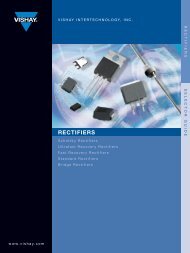
Vishay General Semiconductor<br />
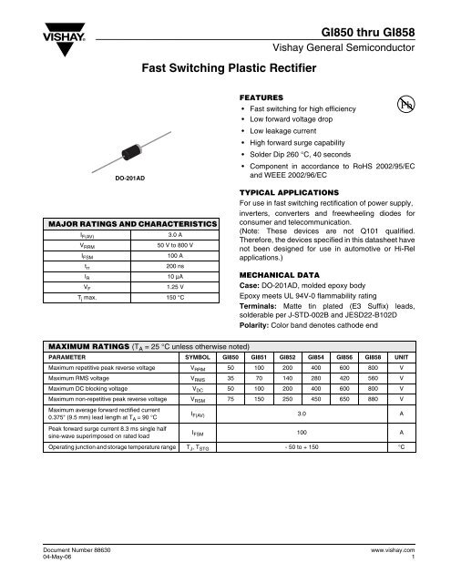
DO-201AD<br />
MAJOR RATINGS AND CHARACTERISTICS<br />
I F(AV)<br />
3.0 A<br />
V RRM<br />
50 V to 800 V<br />
I FSM<br />
100 A<br />
t rr<br />
200 ns<br />
I R 10 µA<br />
V F<br />
1.25 V<br />
T j max. 150 °C<br />
FEATURES<br />
• <strong>Fast</strong> switching for high efficiency<br />
• Low forward voltage drop<br />
• Low leakage current<br />
• High forward surge capability<br />
• Solder Dip 260 °C, 40 seconds<br />
• Component in accordance to RoHS 2002/95/EC<br />
and WEEE 2002/96/EC<br />
TYPICAL APPLICATIONS<br />
For use in fast switching rectification of power supply,<br />
inverters, converters and freewheeling diodes for<br />
consumer and telecommunication.<br />
(Note: These devices are not Q101 qualified.<br />
Therefore, the devices specified in this datasheet have<br />
not been designed for use in automotive or Hi-Rel<br />
applications.)<br />
MECHANICAL DATA<br />
Case: DO-201AD, molded epoxy body<br />
Epoxy meets UL 94V-0 flammability rating<br />
Terminals: Matte tin plated (E3 Suffix) leads,<br />
solderable per J-STD-002B and JESD22-B102D<br />
Polarity: Color band denotes cathode end<br />
MAXIMUM RATINGS (T A = 25 °C unless otherwise noted)<br />
PARAMETER SYMBOL <strong>GI850</strong> GI851 GI852 GI854 GI856 <strong>GI858</strong> UNIT<br />
Maximum repetitive peak reverse voltage V RRM 50 100 200 400 600 800 V<br />
Maximum RMS voltage V RMS 35 70 140 280 420 560 V<br />
Maximum DC blocking voltage V DC 50 100 200 400 600 800 V<br />
Maximum non-repetitive peak reverse voltage V RSM 75 150 250 450 650 880 V<br />
Maximum average forward rectified current<br />
0.375" (9.5 mm) lead length at T A = 90 °C<br />
I F(AV) 3.0 A<br />
Peak forward surge current 8.3 ms single half<br />
sine-wave superimposed on rated load<br />
I FSM 100 A<br />
Operating junction and storage temperature range T J , T STG - 50 to + 150 °C<br />
Document Number 88630<br />
04-May-06<br />
www.vishay.com<br />
1
<strong>GI850</strong> <strong>thru</strong> <strong>GI858</strong><br />
Vishay General Semiconductor<br />
ELECTRICAL CHARACTERISTICS (T A = 25 °C unless otherwise noted)<br />
PARAMETER TEST CONDITIONS SYMBOL <strong>GI850</strong> GI851 GI852 GI854 GI856 <strong>GI858</strong> UNIT<br />
Maximum<br />
instantaneous<br />
forward voltage<br />
at 3.0 A<br />
at 9.4 A, T J = 175 °C<br />
V F<br />
1.25<br />
1.10<br />
V<br />
Maximum DC reverse<br />
current at rated DC<br />
blocking voltage<br />
T A = 25 °C<br />
T A = 100 °C<br />
I R<br />
10<br />
150 150 200 250 300 500<br />
µA<br />
Maximum reverse<br />
recovery time<br />
Maximum reverse<br />
recovery time<br />
Typical junction<br />
capacitance<br />
at I F = 1.0 A, V R = 30 V,<br />
di/dt = 50 A/µs, I rr = 10 % I RM<br />
at I F = 1.0 A, V R = 30 V,<br />
di/dt = 50 A/µs, I rr = 10 % I RM<br />
t rr 200 ns<br />
I RM(REC) 2.0 A<br />
at 4.0 V, 1 MHz C J 28 pF<br />
THERMAL CHARACTERISTICS (T A = 25 °C unless otherwise noted)<br />
PARAMETER SYMBOL <strong>GI850</strong> GI851 GI852 GI854 GI856 <strong>GI858</strong> UNIT<br />
Typical thermal resistance (1)<br />
R θJA<br />
R θJL<br />
Note:<br />
(1) Thermal resistance from junction to ambient and from junction to lead at 0.375" (9.5 mm) lead length, with both leads equally heat sink<br />
22<br />
8.0<br />
°C/W<br />
ORDERING INFORMATION<br />
PREFERRED P/N UNIT WEIGHT (g) PREFERRED PACKAGE CODE BASE QUANTITY DELIVERY MODE<br />
GI856-E3/54 1.1 54 1400 13" Diameter Paper Tape & Reel<br />
GI856-E3/73 1.1 73 1000 Ammo Pack Packaging<br />
RATINGS AND CHARACTERISTICS CURVES<br />
(T A = 25 °C unless otherwise noted)<br />
Average Forward Rectified Current (A)<br />
8.0<br />
6.0<br />
4.0<br />
2.0<br />
TL = Lead Temperature<br />
L = 0.25" (6.3 mm)<br />
L = 0.375" (9.5 mm)<br />
Lead Length<br />
T A =Ambient Temperature<br />
0.375" (9.5 mm) Lead Length<br />
0<br />
30 50 70 90 110 130 150 170<br />
Temperature (°C)<br />
L=Lead Length<br />
0.8 x 0.8 x 0.40"<br />
(20 x 20 x 1 mm)<br />
Copper Heatsinks<br />
Peak Forward Surge Current (A)<br />
200<br />
100<br />
8.3 ms Single Half Sine-Wave<br />
TJ = 25 °C<br />
Non-Repetitive<br />
TJ = 150 °C<br />
TJ = 25 °C<br />
TJ<br />
Repetitive<br />
= 150 °C<br />
10<br />
1 10 100<br />
Number of Cycles at 60 Hz<br />
Figure 1. Forward Current Derating Curves<br />
Figure 2. Maximum Peak Forward Surge Current<br />
www.vishay.com<br />
2<br />
Document Number 88630<br />
04-May-06
<strong>GI850</strong> <strong>thru</strong> <strong>GI858</strong><br />
Vishay General Semiconductor<br />
100<br />
100<br />
Instantaneous Forward Current (A)<br />
10<br />
1<br />
0.1<br />
TJ = 25 °C<br />
Pulse Width = 300 µs<br />
1 % Duty Cycle<br />
Junction Capacitance (pF)<br />
TJ = 25 °C<br />
f = 1.0 MHz<br />
Vsig = 50 mVp-p<br />
0.01<br />
0.4 0.6 0.8 1.0 1.2 1.4 1.6 1.8<br />
Instantaneous Forward Voltage (V)<br />
Figure 3. Typical Instantaneous Forward Characteristics<br />
10<br />
1 10 100<br />
Reverse Voltage (V)<br />
Figure 5. Typical Junction Capacitance<br />
10<br />
Instantaneous Reverse Current (µA)<br />
1<br />
0.1<br />
TJ = 100 °C<br />
TJ = 50 °C<br />
TJ = 25 °C<br />
0.01<br />
0 20 40 60 80 100<br />
Percent of Rated Peak Reverse Voltage (%)<br />
Figure 4. Typical Reverse Characteristics<br />
PACKAGE OUTLINE DIMENSIONS in inches (millimeters)<br />
DO-201AD<br />
0.210 (5.3)<br />
0.190 (4.8)<br />
DIA.<br />
1.0 (25.4)<br />
MIN.<br />
0.375 (9.5)<br />
0.285 (7.2<br />
0.052 (1.32)<br />
0.048 (1.22)<br />
DIA.<br />
1.0 (25.4)<br />
MIN.<br />
Document Number 88630<br />
04-May-06<br />
www.vishay.com<br />
3