SUM110N04-2m7H N-Channel 40-V (D-S) 175_C MOSFET
SUM110N04-2m7H N-Channel 40-V (D-S) 175_C MOSFET
SUM110N04-2m7H N-Channel 40-V (D-S) 175_C MOSFET

Create successful ePaper yourself
Turn your PDF publications into a flip-book with our unique Google optimized e-Paper software.
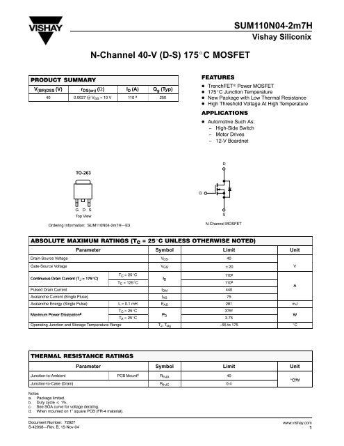
N-<strong>Channel</strong> <strong>40</strong>-V (D-S) <strong>175</strong>C <strong>MOSFET</strong><strong>SUM110N04</strong>-<strong>2m7H</strong>Vishay SiliconixPRODUCT SUMMARYV (BR)DSS (V) r DS(on) () I D (A) Q g (Typ)<strong>40</strong> 0.0027 @ V GS = 10 V 110 a 250FEATURES TrenchFET Power <strong>MOSFET</strong> <strong>175</strong>C Junction Temperature New Package with Low Thermal Resistance High Threshold Voltage At High TemperatureAPPLICATIONS Automotive Such As:− High-Side Switch− Motor Drives− 12-V BoardnetDTO-263GG D STop ViewOrdering Information: <strong>SUM110N04</strong>-<strong>2m7H</strong>—E3SN-<strong>Channel</strong> <strong>MOSFET</strong>ABSOLUTE MAXIMUM RATINGS (T C = 25C UNLESS OTHERWISE NOTED)Parameter Symbol Limit UnitDrain-Source Voltage V DS <strong>40</strong>Gate-Source Voltage V GS 20 VContinuous Drain Current (T J = <strong>175</strong>C)T C = 25CI D110 aT C = 125C110 a APulsed Drain Current I DM 4<strong>40</strong>Avalanche Current (Single Pluse) I AS 75Avalanche Energy (Single Pulse) L = 0.1 mH E AS 281 mJMaximum Power Dissipation bT C = 25CT A = 25CP D375 c3.75WOperating Junction and Storage Temperature Range T J , T stg −55 to <strong>175</strong> CTHERMAL RESISTANCE RATINGSParameter Symbol Limit UnitJunction-to-Ambient PCB Mount d R thJA <strong>40</strong>Junction-to-Case (Drain) R thJC 0.4C/WNotesa. Package limited.b. Duty cycle 1%.c. See SOA curve for voltage derating.d. When mounted on 1” square PCB (FR-4 material).Document Number: 72927S-42058—Rev. B, 15-Nov-04www.vishay.com1
<strong>SUM110N04</strong>-<strong>2m7H</strong>Vishay SiliconixSPECIFICATIONS (T J =25C UNLESS OTHERWISE NOTED)StaticParameter Symbol Test Condition Min Typ Max UnitDrain-Source Breakdown Voltage V (BR)DSS V DS = 0 V, I D = 250 A <strong>40</strong>Gate-Threshold Voltage V GS(th) V DS = V GS , I D = 250 A 3.4 4.5VGate-Body Leakage I GSS V DS = 0 V, V GS = 20 V 100 nAV DS = <strong>40</strong> V, V GS = 0 V 1Zero Gate Voltage Drain Current I DSSV DS = <strong>40</strong> V, V GS = 0 V, T J = 125C 50 AV DS = <strong>40</strong> V, V GS = 0 V, T J = <strong>175</strong>C 250On-State Drain Current a I D(on) V DS 5 V, V GS = 10 V 120 AV GS = 10 V, I D = 30 A 0.0022 0.0027Drain-Source On-State Resistance a r DS(on) V GS = 10 V, I D = 30 A, T J = 125C 0.0042 DS(on)V GS = 10 V, I D = 30 A, T J = <strong>175</strong>C 0.0052Forward Transconductance a g fs V DS = 15 V, I D = 30 A 30 SDynamic bInput Capacitance C iss 15720Output Capacitance C oss V GS = 0 V, V DS = 25 V, f = 1 MHz 1<strong>40</strong>0 pFReverse Transfer Capacitance C rss 800Gate Resistance R g f = 1.0 MHz 1.2 Total Gate Charge c Q g 250 375Gate-Source Charge c Q gs V DS = 30 V, V GS = 10 V, I D = 110 A 95 nCGate-Drain Charge c Q gdDS , GS , D57Turn-On Delay Time c t d(on) 50 75Rise Time c t r V DD = 30 V, R L = 0.27 150 225Turn-Off Delay Time c t d(off)I D 110 A, V GEN = 10 V, R g = 2.5 70 105Fall Time c t f 25 <strong>40</strong>nsSource-Drain Diode Ratings and Characteristics (T C = 25C) bContinuous Current I S 110Pulsed Current I SM 2<strong>40</strong>AForward Voltage a V SD I F = 85 A, V GS = 0 V 1.1 1.5 VReverse Recovery Time t rr 65 100 nsPeak Reverse Recovery Current I RM(REC) I F = 85 A, di/dt = 100 A/s 2.8 4.2 AReverse Recovery Charge Q rr 0.091 0.21 CNotesa. Pulse test; pulse width 300 s, duty cycle 2%.b. Guaranteed by design, not subject to production testing.c. Independent of operating temperature.Stresses beyond those listed under “Absolute Maximum Ratings” may cause permanent damage to the device. These are stress ratings only, and functional operationof the device at these or any other conditions beyond those indicated in the operational sections of the specifications is not implied. Exposure to absolute maximum ratingconditions for extended periods may affect device reliability.www.vishay.com2Document Number: 72927S-42058—Rev. B, 15-Nov-04
<strong>SUM110N04</strong>-<strong>2m7H</strong>Vishay SiliconixTYPICAL CHARACTERISTICS (25C UNLESS NOTED)250Output Characteristics250Transfer Characteristics200V GS = 10 thru 7 V200− Drain Current (A)1501006 V− Drain Current (A)150100I DI DT C = 125C504 V 5 V00 2 4 6 8 10V DS − Drain-to-Source Voltage (V)5025C−55C00 1 2 3 4 5 6 7V GS − Gate-to-Source Voltage (V)350TransconductanceT C = −55C0.005On-Resistance vs. Drain Current− Transconductance (S)g fs2802101<strong>40</strong>7025C125Cr DS(on) − On-Resistance ( )0.00<strong>40</strong>.0030.0020.001V GS = 10 V00 20 <strong>40</strong> 60 80 100I D − Drain Current (A)0.0000 20 <strong>40</strong> 60 80 100 120I D − Drain Current (A)20000Capacitance20Gate ChargeC − Capacitance (pF)16000120008000<strong>40</strong>00C ossC rssC iss− Gate-to-Source Voltage (V)V GS161284V DS = 30 VI D = 110 A00 8 16 24 32 <strong>40</strong>V DS − Drain-to-Source Voltage (V)00 100 200 300 <strong>40</strong>0 500Q g − Total Gate Charge (nC)Document Number: 72927S-42058—Rev. B, 15-Nov-04www.vishay.com3
<strong>SUM110N04</strong>-<strong>2m7H</strong>Vishay SiliconixTYPICAL CHARACTERISTICS (25C UNLESS NOTED)2.0On-Resistance vs. Junction Temperature100Source-Drain Diode Forward Voltage1.8V GS = 10 VI D = 30 Ar DS(on) − On-Resiistance(Normalized)1.61.41.21.00.8− Source Current (A)I S10T J = 150CT J = 25C0.60.4−50 −25 0 25 50 75 100 125 150 <strong>175</strong>T J − Junction Temperature (C)100.3 0.6 0.9 1.2V SD − Source-to-Drain Voltage (V)1000Avalanche Current vs. Time52Drain Source Breakdown vs.Junction Temperature10050I D = 10 mA(a)I Dav10I AV (A) @ T A = 25CV (BR)DSS (V)4846I AV (A) @ T A = 150C441420.10.00001 0.0001 0.001 0.01 0.1 1t in (Sec)<strong>40</strong>−50 −25 0 25 50 75 100 125 150 <strong>175</strong>T J − Junction Temperature (C)www.vishay.com4Document Number: 72927S-42058—Rev. B, 15-Nov-04
<strong>SUM110N04</strong>-<strong>2m7H</strong>Vishay SiliconixTHERMAL RATINGS300Maximum Avalanche and Drain Currentvs. Case Temperature1000Safe Operating Area a250*Limited by r DS(on)10 s100100 s− Drain Current (A)200150100− Drain Current (A)101 ms10 msdc, 100 msI D50Limited By PackageI D1T C = 25CSingle Pulse00 25 50 75 100 125 150 <strong>175</strong>T C − Case Temperature (C)0.10.1 1 10 100V DS − Drain-to-Source Voltage (V)*V GS minimum V GS at which r DS(on) is specified2Normalized Thermal Transient Impedance, Junction-to-CaseNormalized Effective TransientThermal Impedance10.1Duty Cycle = 0.50.20.050.02Single Pulse0.10.0110 −4 10 −3 10 −2 10 −1Square Wave Pulse Duration (sec)1Notesa. V GS minimum V GS at which r DS(on) iis specified.Vishay Siliconix maintains worldwide manufacturing capability. Products may be manufactured at one of several qualified locations. Reliability data for Silicon Technology andPackage Reliability represent a composite of all qualified locations. For related documents such as package/tape drawings, part marking, and reliability data, seehttp://www.vishay.com/ppg?72927.Document Number: 72927S-42058—Rev. B, 15-Nov-04www.vishay.com5