SUM110N04-2m7H N-Channel 40-V (D-S) 175_C MOSFET
SUM110N04-2m7H N-Channel 40-V (D-S) 175_C MOSFET
SUM110N04-2m7H N-Channel 40-V (D-S) 175_C MOSFET

Create successful ePaper yourself
Turn your PDF publications into a flip-book with our unique Google optimized e-Paper software.
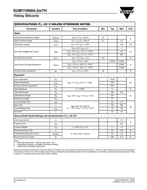
<strong>SUM110N04</strong>-<strong>2m7H</strong>Vishay SiliconixSPECIFICATIONS (T J =25C UNLESS OTHERWISE NOTED)StaticParameter Symbol Test Condition Min Typ Max UnitDrain-Source Breakdown Voltage V (BR)DSS V DS = 0 V, I D = 250 A <strong>40</strong>Gate-Threshold Voltage V GS(th) V DS = V GS , I D = 250 A 3.4 4.5VGate-Body Leakage I GSS V DS = 0 V, V GS = 20 V 100 nAV DS = <strong>40</strong> V, V GS = 0 V 1Zero Gate Voltage Drain Current I DSSV DS = <strong>40</strong> V, V GS = 0 V, T J = 125C 50 AV DS = <strong>40</strong> V, V GS = 0 V, T J = <strong>175</strong>C 250On-State Drain Current a I D(on) V DS 5 V, V GS = 10 V 120 AV GS = 10 V, I D = 30 A 0.0022 0.0027Drain-Source On-State Resistance a r DS(on) V GS = 10 V, I D = 30 A, T J = 125C 0.0042 DS(on)V GS = 10 V, I D = 30 A, T J = <strong>175</strong>C 0.0052Forward Transconductance a g fs V DS = 15 V, I D = 30 A 30 SDynamic bInput Capacitance C iss 15720Output Capacitance C oss V GS = 0 V, V DS = 25 V, f = 1 MHz 1<strong>40</strong>0 pFReverse Transfer Capacitance C rss 800Gate Resistance R g f = 1.0 MHz 1.2 Total Gate Charge c Q g 250 375Gate-Source Charge c Q gs V DS = 30 V, V GS = 10 V, I D = 110 A 95 nCGate-Drain Charge c Q gdDS , GS , D57Turn-On Delay Time c t d(on) 50 75Rise Time c t r V DD = 30 V, R L = 0.27 150 225Turn-Off Delay Time c t d(off)I D 110 A, V GEN = 10 V, R g = 2.5 70 105Fall Time c t f 25 <strong>40</strong>nsSource-Drain Diode Ratings and Characteristics (T C = 25C) bContinuous Current I S 110Pulsed Current I SM 2<strong>40</strong>AForward Voltage a V SD I F = 85 A, V GS = 0 V 1.1 1.5 VReverse Recovery Time t rr 65 100 nsPeak Reverse Recovery Current I RM(REC) I F = 85 A, di/dt = 100 A/s 2.8 4.2 AReverse Recovery Charge Q rr 0.091 0.21 CNotesa. Pulse test; pulse width 300 s, duty cycle 2%.b. Guaranteed by design, not subject to production testing.c. Independent of operating temperature.Stresses beyond those listed under “Absolute Maximum Ratings” may cause permanent damage to the device. These are stress ratings only, and functional operationof the device at these or any other conditions beyond those indicated in the operational sections of the specifications is not implied. Exposure to absolute maximum ratingconditions for extended periods may affect device reliability.www.vishay.com2Document Number: 72927S-42058—Rev. B, 15-Nov-04