TFDU4203 Integrated Low Profile Transceiver Module for Telecom ...
TFDU4203 Integrated Low Profile Transceiver Module for Telecom ...
TFDU4203 Integrated Low Profile Transceiver Module for Telecom ...

You also want an ePaper? Increase the reach of your titles
YUMPU automatically turns print PDFs into web optimized ePapers that Google loves.
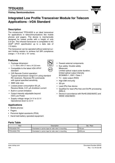
<strong>TFDU4203</strong>Vishay Semiconductors<strong>Integrated</strong> <strong>Low</strong> <strong>Profile</strong> <strong>Transceiver</strong> <strong>Module</strong> <strong>for</strong> <strong>Telecom</strong>Applications - IrDA StandardDescriptionThe miniaturized <strong>TFDU4203</strong> is an ideal transceiver<strong>for</strong> applications in telecommunications like mobilephones and pagers. The device is mechanicallydesigned <strong>for</strong> lowest profile with a height of only2.8 mm. The infrared transceiver is compatible to theIrDA ® IrPHY specification up to a data rate of115 kbit/s.The transceiver can be operated without external currentlimiting resistor to achieve full SIR compliance(range > 1 m in full ± 15° cone).18170Features• Package dimension:L 7.1 mm x W 4.7 mm x H 2.8 mm• Compatible to the latest IrDA IrPHYstandard• CIR Remote Control operation:Typical transmission range 8 m using standardRC-receivers. Receives RC-commandswith typical specified sensitivity.• SMD side view• <strong>Low</strong>est power consumption 65 µA,Receive Mode, 0.01 µA shutdown current• Built-in current limitation• Output intensity adjustable beyondIrDA <strong>Low</strong> Power• Supply voltage range 2.4 V to 5.5 VOperational down to 2.0 Ve3• Fewest external components• Eye safety: Double safetyMeasures:Limited optical output pulse duration,limited optical output intensityIEC60825-1, 2001: Class 1• Tri - state output (RXD)• High EMI immunity• SD pin• Lead (Pb)-free device• Qualified <strong>for</strong> lead (Pb)-free and Sn/Pb processing(MSL4)• Device in accordance with RoHS 2002/95/EC andWEEE 2002/96/ECApplications• Mobile phones• Pagers• Personal digital assistants (PDA)• Hand-held battery operated equipmentParts TablePart Description Qty / Reel<strong>TFDU4203</strong>-TR1 Orientated in carrier tape <strong>for</strong> side view in mounting 750 pcs<strong>TFDU4203</strong>-TR3 Orientated in carrier tape <strong>for</strong> side view in mounting 2250 pcswww.vishay.com194Document Number 82542Rev. 1.6, 04-Oct-06
<strong>TFDU4203</strong>Vishay SemiconductorsEye safety in<strong>for</strong>mationVirtual source size(<strong>TFDU4203</strong> only)Parameter Test Conditions Symbol Min Typ. Max UnitMethod: (1 - 1/e) encircledenergyd 2 mmCompatible to Class 1 operation of IEC 60825 or EN60825 with worst case IrDA SIR pulse pattern, 115.2 kbit/sElectrical Characteristics<strong>Transceiver</strong>Parameter Test Conditions Symbol Min Typ. Max UnitSupported data rates base band 9.6 115.2 kbit/sSupply voltage range operational down to 2.0 V V CC 2.4 5.5 VSupply current V CC = 2.4 V to 5.5 V, E e = 0,receive mode, full temperaturerangeI S 65 100 µASupply current, at V CCPIRED peak current transmitting<strong>Transceiver</strong> ‘power on‘ settlingtimeV CC = 2.4 V to 5.5 V, 10 klxsunlight, receive mode ortransmit mode,full temperature range,no signalV CC = 2.7 V 115.2 kbit/stransmission, receive mode,nose to nose operationI S 70 100 µAI S 1 mAshutdown mode, entireI Sshdown 0.02 1 µAtemperature rangeV CC = 5.5 V, 20 °C I Sshdown 10 nAI e = 40 mW/sr,I Str 360 mAno external resistorV CCP = 2.7 V, equivalent to SIRstandardtime from switching on V CCto established specifiedoperation1 mswww.vishay.com196Document Number 82542Rev. 1.6, 04-Oct-06
<strong>TFDU4203</strong>Vishay SemiconductorsOptoelectronic CharacteristicsReceiverTested <strong>for</strong> the following parameters (V CC = 2.4 V to 5.5 V, - 25 °C to + 85 °C, unless otherwise stated).Parameter Test Conditions Symbol Min Typ. Max UnitMinimum detection thresholdirradiance (logic high receiverinput irradiance)Maximum detection thresholdirradiance| α | ≤ ± 15 °,V CC = 2.0 V to 5.5 VE e, min 25(2.5)50(5)mW/m 2(µW/cm 2 )2.0 V, 25 °C tested E e, min 50 100 mW/m 2| α | ≤ ± 90 °, V CC = 5 V E e, max 3300(330)| α | ≤ ± 90 °, V CC = 3 V E e, max 8000(800)5000(500)15000(1500)W/cm 2(µW/cm 2 )W/cm 2(µW/cm 2 )Logic low receiver inputirradianceE e, max,low 4(0.4)mW/m 2(µW/cm 2 )Output voltage RXD active, C = 15 pF V OL 0 0.5 Vnon active, C = 15 pF V OH V CC - 0.5 VOutput current RXD V OL < 0.5 V 4 mARise time at load C = 15 pF, R = 2.2 kΩ t r 20 70 nsFall time at load C = 15 pF, R = 2.2 kΩ t f 20 70 nsRxd signal electrical outputpulse widthOutput delay time (RXD),leading edge optical input toelectrical outputJitter, leading edge of outputsignalOutput delay time (RXD), trailingedge optical input to electricaloutput2.4 kbit/s, input pulse width1.41 µs to 3/16 of bit duration115.2 kbit/s, input pulse width1.41 µs to 3/16 of bit durationt p 1.41 20 µst p 1.41 4.5 µsoutput level =t dl 1 2 µs0.5 x V CC at 40 mW/m 2over a period of 10 bit,115.2 kbit/st j 400 nsoutput level =t dt 6.5 µs0.5 x V CC at 40 mW/m 2Power on time, SD recovery0.1 1 mstimeLatency t L 100 200 µsDocument Number 82542Rev. 1.6, 04-Oct-06www.vishay.com197
<strong>TFDU4203</strong>Vishay SemiconductorsTransmitterParameter Test Conditions Symbol Min Typ. Max UnitLogic low shutdown inputV IL(TXD) - 0.5 0.15 x V CC Vvoltage *)Logic high shutdown inputV IH(TXD) 0.8 x V CC 6 Vvoltage *)Logic low transmitter inputV IL(TXD) 0.5 0.81 x V CC Vvoltage *)Logic high transmitter inputV IH(TXD) 0.8 x V CC 6 Vvoltage *)Optical output radiant intensity | α | ≤ ± 15 °, I F1 = 320 mA,I e 45 mW/srvoltage range 2.7 V to 5.5 V *)Internally current controlled **) ,Peak emission wavelength λ p 880 900 nmSpectral emission bandwidth 40 nmOptical rise/fall time115.2 kHz square wave signal200 ns(duty cycle 1 : 1)Optical output pulse duration input pulse duration 1.6 µs 1.5 1.6 1.7 µsOutput radiant intensity logic low level 0.04 µW/srOvershoot, optical 25 %Rising edge peak to peak jitter over a period of 10 bits,t j 0.2 µsindependent of in<strong>for</strong>mationcontent*) Recommended logic levels <strong>for</strong> minimum shutdown current. The CMOS decision level is 0.5 x V CC.** ) Add external resistor <strong>for</strong> V CC > 4 V to prevent thermal overload, see Fig. 3.Truth tableInputsOutputsSD TXD Optical input Irradiance mW/m 2 RXD Transmitterhigh x x floating 0low high x high I elow high ≥ 25 µs x high 0low low < 4 high 0low low > Min. Detection Threshold Irradiance x 0low low > Max. Detection Threshold Irradiance x 0Application HintsThe <strong>TFDU4203</strong> does not need any external componentswhen operated with a "clean" power supply. Ina more noisy ambient it is recommended to add acapacitor C1 (4.7 µF Tantalum) and a resistor R1(≤ 3 Ω) <strong>for</strong> noise suppression. In addition the capacitoris needed to prevent a pulse distortion when thepower supply is not able to generate the peak currentsor inductive wiring is used. A combination of atantalum with a ceramics capacitor will be efficient toattenuate both, RF and LF if RF noise is present. Thevalue is dependent on the power supply quality. Agood choice is between 4.7 µF and 10 µF.Shut downTo shut down the <strong>TFDU4203</strong> into a standby mode theSD pin has to be set active.LatencyThe receiver is in specified conditions after thedefined latency.In a UART related application after that time after thelast transmitted signal (IrDA specifies 500 µs maximum<strong>for</strong> low power applications and 10 ms maximum<strong>for</strong> standard) the receiver buffer of the UART must becleared. There<strong>for</strong>e the transceiver has to wait at leastthe specified latency after receiving the last bit be<strong>for</strong>estarting the transmission to be sure that the correspondingreceiver is in a defined state.For more application circuits, see IrDC Design Guideand TOIM4232 data sheet.www.vishay.com198Document Number 82542Rev. 1.6, 04-Oct-06
<strong>TFDU4203</strong>Vishay SemiconductorsRecommended Circuit DiagramSD8SDGND5, 6 GNDRXD3RXDTXDVccR1C1R27 TXD4 V CC1, 2 IRED Cathode18199Recommended Application Circuit ComponentsComponent Recommended Value Vishay Part NumberC1 4.7 µF, 16 V 293D 475X9 016B 2TR15 Ω maxThis is a recommendation <strong>for</strong> a combination to start with to exclude power supply effects.Optimum, from a costs point of view, to work without both.Temperature Derating DiagramAmbient Temperature (°C )9085807570656055502.0 2.5 3.0 3.5 4.0 4.5 5.0 5.5 6.018097Operating Voltage [V] at duty cycle 20 %Figure 1. Temperature Derating DiagramThe temperature derating diagram shows the maximumoperating temperature when the device is operatedwithout external current limiting resistor. A powerdissipating resistor of 2 Ω is recommended from thecathode of the IRED to Ground <strong>for</strong> supply voltagesabove 4 V. In that case the device can be operated upto 85 °C, too.Document Number 82542Rev. 1.6, 04-Oct-06www.vishay.com199
<strong>TFDU4203</strong>Vishay SemiconductorsRecommended Solder <strong>Profile</strong>sSolder <strong>Profile</strong> <strong>for</strong> Sn/Pb SolderingTemperature (°C)260240220200180160140120100806040200195352...4 °C/s240 °C max.160 °C max.120 s...180 s2...4 °C/s10 s max. at 230 °C90 s max.0 50 100 150 200 250 300 350Time/sFigure 2. Recommended Solder <strong>Profile</strong> <strong>for</strong> Sn/Pb solderingLead (Pb)-Free, Recommended Solder <strong>Profile</strong>The <strong>TFDU4203</strong> is a lead (Pb)-free transceiver andqualified <strong>for</strong> lead (Pb)-free processing. For lead (Pb)-free solder paste like Sn (3.0 - 4.0) Ag (0.5 - 0.9) Cu,there are two standard reflow profiles: Ramp-Soak-Spike (RSS) and Ramp-To-Spike (RTS). The Ramp-Soak-Spike profile was developed primarily <strong>for</strong> reflowovens heated by infrared radiation. With widespreaduse of <strong>for</strong>ced convection reflow ovens the Ramp-To-Spike profile is used increasingly. Shown below in figure3 and 4 are VISHAY's recommended profiles <strong>for</strong>use with the <strong>TFDU4203</strong> transceivers. For moredetails please refer to the application note“SMD Assembly Instructions”(http://www.vishay.com/docs/82602/82602.pdf).A ramp-up rate less than 0.9 °C/s is not recommended.Ramp-up rates faster than 1.3 °C/s coulddamage an optical part because the thermal conductivityis less than compared to a standard IC.Wave SolderingFor TFDUxxxx and TFBSxxxx transceiver deviceswave soldering is not recommended.StorageThe storage and drying processes <strong>for</strong> all VISHAYtransceivers (TFDUxxxx and TFBSxxx) are equivalentto MSL4.The data <strong>for</strong> the drying procedure is given on labelson the packing and also in the application note"Taping, Labeling, Storage and Packing"(http://www.vishay.com/docs/82601/82601.pdf).Temperature/°C19532Temperature/°C2752502252001751501251007550252802602402202001801601401201008060402002 °C...3 °C/sT ≥ 255 °C <strong>for</strong> 10 s....30 sT ≥ 217 °C <strong>for</strong> 70 s max90 s...120 s30 s max.70 s max.0 50 100 150 200 250 300 350Time/sFigure 3. Solder <strong>Profile</strong>, RSS RecommendationT peak = 260 °C max1.3 °C/sTime above 217 °C t ≤ 70 sTime above 250 °C t ≤ 40 sPeak temperature T peak = 260 °C< 4 °C/sFigure 4. RTS RecommendationT peak = 260 °C2 °C...4 °C/s< 2 °C/s00 50 100 150 200 250 300Time/sManual SolderingManual soldering is the standard method <strong>for</strong> lab use.However, <strong>for</strong> a production process it cannot be recommendedbecause the risk of damage is highlydependent on the experience of the operator. Nevertheless,we added a chapter to the above mentionedapplication note, describing manual soldering anddesoldering.www.vishay.com200Document Number 82542Rev. 1.6, 04-Oct-06
<strong>TFDU4203</strong>Vishay SemiconductorsPackage Dimensions19821Drawing-No.: 6.550-5185.01-4Issue: 5; 02.09.05Figure 5. Package drawing, <strong>TFDU4203</strong>Document Number 82542Rev. 1.6, 04-Oct-06www.vishay.com201
<strong>TFDU4203</strong>Vishay SemiconductorsReel DimensionsDrawing-No.: 9.800-5090.01-4Issue: 1; 29.11.0514017mm mm mm mm mm mm mmTape Width A max. N W 1 min. W 2 max. W 3 min. W 3 max.16 180 60 16.4 22.4 15.9 19.416 330 50 16.4 22.4 15.9 19.4www.vishay.com202Document Number 82542Rev. 1.6, 04-Oct-06
<strong>TFDU4203</strong>Vishay SemiconductorsTape Dimensions19820Drawing-No.: 9.700-5227.01-4Issue: 3; 03.09.99Figure 6. Tape drawing, <strong>TFDU4203</strong> <strong>for</strong> side view mountingDocument Number 82542Rev. 1.6, 04-Oct-06www.vishay.com203
VISHAY<strong>TFDU4203</strong>Vishay SemiconductorsOzone Depleting Substances Policy StatementIt is the policy of Vishay Semiconductor GmbH to1. Meet all present and future national and international statutory requirements.2. Regularly and continuously improve the per<strong>for</strong>mance of our products, processes, distribution and operatingsystems with respect to their impact on the health and safety of our employees and the public, as well astheir impact on the environment.It is particular concern to control or eliminate releases of those substances into the atmosphere which areknown as ozone depleting substances (ODSs).The Montreal Protocol (1987) and its London Amendments (1990) intend to severely restrict the use of ODSsand <strong>for</strong>bid their use within the next ten years. Various national and international initiatives are pressing <strong>for</strong> anearlier ban on these substances.Vishay Semiconductor GmbH has been able to use its policy of continuous improvements to eliminate the useof ODSs listed in the following documents.1. Annex A, B and list of transitional substances of the Montreal Protocol and the London Amendmentsrespectively2. Class I and II ozone depleting substances in the Clean Air Act Amendments of 1990 by the EnvironmentalProtection Agency (EPA) in the USA3. Council Decision 88/540/EEC and 91/690/EEC Annex A, B and C (transitional substances) respectively.Vishay Semiconductor GmbH can certify that our semiconductors are not manufactured with ozone depletingsubstances and do not contain such substances.We reserve the right to make changes to improve technical designand may do so without further notice.Parameters can vary in different applications. All operating parameters must be validated <strong>for</strong> eachcustomer application by the customer. Should the buyer use Vishay Semiconductors products <strong>for</strong> anyunintended or unauthorized application, the buyer shall indemnify Vishay Semiconductors against allclaims, costs, damages, and expenses, arising out of, directly or indirectly, any claim of personaldamage, injury or death associated with such unintended or unauthorized use.Vishay Semiconductor GmbH, P.O.B. 3535, D-74025 Heilbronn, GermanyDocument Number 82542Rev. 1.6, 04-Oct-06www.vishay.com204