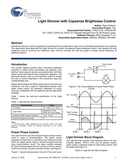
Light Dimmer with Capsense Brightness Control
Light Dimmer with Capsense Brightness Control
Light Dimmer with Capsense Brightness Control

You also want an ePaper? Increase the reach of your titles
YUMPU automatically turns print PDFs into web optimized ePapers that Google loves.
Abstract<br />
<strong>Light</strong> <strong>Dimmer</strong> <strong>with</strong> <strong>Capsense</strong> <strong>Brightness</strong> <strong>Control</strong><br />
Author: Petro Koblyuk<br />
Associated Project: Yes<br />
Associated Part Family: CY8C21x34, CY8C24x94<br />
GET FREE SAMPLES HERE (CY Sample Request Form for all Product Lines)<br />
Software Version: PSoC Designer 4.4<br />
Associated Application Notes: AN2302, AN2394, AN13943<br />
Sometimes there is a need to regulate the incandescent lamp brightness to gain more comfortable and pleasant room lighting.<br />
This Application Note describes the <strong>Light</strong> <strong>Dimmer</strong> for smooth incandescent lamp brightness control. User adjusts the lamp<br />
brightness level by touching the CapSense slider. <strong>Dimmer</strong> includes the LED bar graph to display actual brightness as<br />
additional feature.<br />
Introduction<br />
Triac <strong>Control</strong><br />
The modern lighting systems allow controlling brightness<br />
smoothly to obtain more comfortable and pleasant room<br />
lighting. Some popular devices use potentiometer <strong>with</strong> triac<br />
phase control technique for lamp brightness regulation. The<br />
proposed dimmer uses a touch-sensitive control to enable<br />
the user to control brightness in the convenient, easy and<br />
understandable way.<br />
110-220V,<br />
AC~<br />
Triac<br />
Lamp<br />
Design demonstrates the PSoC ability doing more than only<br />
<strong>Capsense</strong>: one chip is used for capacitance sensing, lamp<br />
power phase control, AC frequency calibration for worldwide<br />
use, multiplexed LED bar graph driving <strong>with</strong> night slight<br />
backlight.<br />
Table 1 shows the technical specification of the <strong>Light</strong><br />
<strong>Dimmer</strong>.<br />
Table 1. <strong>Light</strong> <strong>Dimmer</strong> Specifications<br />
Characteristic<br />
AC Supply<br />
Lamp Power<br />
CapSense Slider Overlay Thickness 1<br />
Quantity of <strong>Brightness</strong> Levels 17<br />
Value<br />
110 – 220 V, 47 – 63 Hz<br />
Depending on triac,<br />
200W for current design<br />
1 mm – 6 mm<br />
Notes<br />
1. The silicon glass, ABS, plexiglass can be used for overlay. The slider<br />
segments dimensions should be adjusted accordingly to the overlay<br />
thickness.<br />
Figure 2. The Timing Diagram of Lamp Power Phase<br />
<strong>Control</strong><br />
AC 110-220V<br />
AC<br />
Zero Crossing<br />
Triac Turning-<br />
On Pulses<br />
Lamp<br />
Waveform<br />
t<br />
t<br />
t<br />
t<br />
Power Phase <strong>Control</strong><br />
The <strong>Light</strong> <strong>Dimmer</strong> uses the principal of power phase control,<br />
which is easy in implementation. The phase control<br />
operation principle lies in controlling triac turning on phase<br />
<strong>with</strong>in AC supply period. Figure 1 shows the typical triac and<br />
lamp interconnection circuit. The delay variation between<br />
AC Zero Crossing signal and triac turning on time is used to<br />
control the amount of power provided to lamp, see Figure 2.<br />
Figure 1. Typical Interconnection Circuit of Triac and Lamp<br />
Delay 1 Delay 2 Delay 3<br />
<strong>Light</strong> <strong>Dimmer</strong> Block Diagram<br />
The <strong>Light</strong> <strong>Dimmer</strong> consists of the following blocks: AC zero<br />
crossing detector, PSoC’s CPU core for general control,<br />
power supply, CapSense slider for load power control, LED<br />
bar graph (see Figure 3).<br />
Figure 3. <strong>Light</strong> <strong>Dimmer</strong> Block Diagram<br />
January 10, 2008 Document No. 001-08990 Rev. *B (AN# is same as last 5 digits of doc #.) 1
Error! Reference source not found.<br />
AC~<br />
Lamp<br />
Triac <strong>Control</strong><br />
AC Zero<br />
Crossing<br />
Zero Crossing<br />
Power Supply<br />
220V AC to 5V DC<br />
Vcc<br />
PSoC<br />
triggering prevention when noised AC signal is close to zero,<br />
the D 4 limits the reverse voltage applied to Q 2 base-emitter<br />
junction, R 17 is zero-crossing detector pull-up. The zerocross<br />
detection operation is shown on Figure 4<br />
Figure 4. The Timing Diagram of “Zero Crossing” Signal<br />
110-220V, AC ~<br />
t<br />
User<br />
Interface<br />
<strong>Capsense</strong><br />
Slider<br />
LED Bar<br />
Graph<br />
Zero Crossing<br />
t<br />
<strong>Dimmer</strong> Hardware<br />
Figure 5 shows the <strong>Light</strong> <strong>Dimmer</strong> schematic. The R 4…R 7<br />
resistors are used for limiting of Q 2 base current, C 9 and<br />
R 4…R 7 form the LPF for zero-crossing detector false<br />
POWER BOARD<br />
Figure 5. <strong>Light</strong> <strong>Dimmer</strong> Schematic<br />
Power Supply<br />
J2<br />
1<br />
2<br />
AC main con<br />
F1<br />
FUSE<br />
D2<br />
1N4007<br />
C3<br />
4.7uF 400V<br />
+<br />
5<br />
4<br />
D<br />
U1<br />
B<br />
F<br />
3<br />
P<br />
B<br />
S 2<br />
S 1<br />
S<br />
LNK304<br />
8 C1<br />
0.1uF<br />
S 7<br />
R1 12k 1%<br />
R2<br />
2k 1%<br />
+ C2<br />
10uF 35V<br />
L1<br />
1mH 280mA<br />
D3<br />
UF4005<br />
D1<br />
1N4007<br />
R3<br />
3.3k<br />
+ C4<br />
100uF<br />
+11.5V<br />
+5V<br />
U2 LP2950/TO92<br />
3<br />
1<br />
IN OUT<br />
D<br />
N<br />
G<br />
C5<br />
2<br />
1uF<br />
C6<br />
1uF<br />
VCC<br />
C7<br />
0.1uF<br />
J1<br />
Lamp con<br />
Q1<br />
MAC15<br />
1<br />
2 R5 107k 0.5W<br />
C8<br />
0.47uF<br />
Triac <strong>Control</strong><br />
R10<br />
10E<br />
Triac<strong>Control</strong><br />
AC Zero Crossing Detector<br />
R4 107k 0.5W<br />
R6 107k 0.5W<br />
R7 107k 0.5W<br />
C9<br />
470pF<br />
VCC<br />
R17 4.7k<br />
D4<br />
LL4148<br />
ZeroCrossing<br />
Q2<br />
BC847<br />
CAPSENSE BOARD<br />
CapSense Slider<br />
SEGMENT1<br />
SEGMENT2<br />
SEGMENT3<br />
SEGMENT4<br />
SEGMENT5<br />
SEGMENT6<br />
SEGMENT7<br />
SEGMENT8<br />
SEGMENT9<br />
LED Bargraph<br />
0 X 1<br />
X 2<br />
X<br />
D<br />
D<br />
D<br />
E<br />
E<br />
E<br />
L<br />
L<br />
L<br />
R11<br />
R12<br />
255E<br />
255E<br />
D20 LED D11 LED<br />
D5 LED D8 LED<br />
R24<br />
R15<br />
R18<br />
R19<br />
R20<br />
R21<br />
R22<br />
R23<br />
R16<br />
R13<br />
255E<br />
D15 LED<br />
D12 LED<br />
X 3<br />
D<br />
E<br />
L<br />
1k<br />
1k<br />
1k<br />
1k<br />
1k<br />
1k<br />
1k<br />
1k<br />
1k<br />
R14<br />
255E<br />
D19 LED<br />
D16 LED<br />
sl0<br />
sl1<br />
sl2<br />
sl3<br />
sl4<br />
sl5<br />
sl6<br />
sl7<br />
sl8<br />
LED Y0<br />
LED Y1<br />
PSoC's CPU Core<br />
LED Y3<br />
LED Y2<br />
LED Y1<br />
LED Y0<br />
ZeroCrossing<br />
Triac<strong>Control</strong><br />
R26<br />
C10<br />
0.1uF<br />
VCC<br />
2 1 0 9 8 7 6 5<br />
3 3 3 2 2 2 2 2<br />
V ss V dd<br />
1<br />
P 0[3] P 0[5] P 0[7] P 0[6] P 0[4] P 0[2]<br />
2<br />
P0[1]<br />
3<br />
P2[7]<br />
4<br />
P2[5]<br />
U3<br />
5<br />
P2[3]<br />
CY8C21434<br />
6<br />
P2[1]<br />
7<br />
P3[3]<br />
8<br />
P3[1]<br />
P1[7]<br />
2k<br />
P 1[5] P 1[3] P 1[1] V ss P 1[0] P 1[2] P 1[4] P 1[6]<br />
9 0 1 2 3 4 5 6<br />
1<br />
1 1 1 1 1<br />
24<br />
P0[0]<br />
23<br />
P2[6]<br />
22<br />
P2[4]<br />
21<br />
P2[2]<br />
20<br />
P2[0]<br />
19<br />
P3[2]<br />
18<br />
P3[0]<br />
XRES 17<br />
sl8<br />
sl7<br />
LED X3<br />
sl6<br />
sl5<br />
sl4<br />
LED X2<br />
LED X1<br />
sl3<br />
sl2<br />
sl1<br />
LED X0<br />
sl0<br />
D6 LED<br />
D9 LED<br />
D13 LED<br />
D17 LED<br />
D7 LED<br />
D10 LED<br />
D14 LED<br />
D18 LED<br />
LED Y2<br />
LED Y3<br />
C13<br />
0.1uF<br />
C L<br />
S<br />
D A<br />
S<br />
January 10, 2008 Document No. 001-08990 Rev. *B (AN# is same as last 5 digits of doc #.) 2
Error! Reference source not found.<br />
Power Supply<br />
A dimmer power supply is implemented using the<br />
transformer-free switching DC-DC regulator, type LNK304<br />
from Power Integrations [1]. The F 1 self-recovered fuse<br />
serves two functions: it protects from possible over<br />
currents and its resistance (about 8 Ohms) limits the C 3<br />
inrush current at power-on. The values of R 1-R 2 divider<br />
define the U 1 regulator output voltage, it is about 11.5 V.<br />
The U 1 output voltage can vary <strong>with</strong> input voltage change<br />
and load current variations. Usage of CapSense requires<br />
stable PSoC power supply [2]. That is why the additional<br />
U 2 linear regulator has been used to form the clear 5 V<br />
supply.<br />
Triac <strong>Control</strong><br />
Triac is driven by short pulses for power consumption<br />
optimization. These pulses are generated by PSoC and<br />
are differentiated by C 8R 10 network. Triac is turned on by<br />
series from 3 pulses, see Figure 6. At full brightness triac<br />
turning on time is some delayed from zero-crossing event<br />
to guarantee reaching the minimum triac turning on<br />
voltage. This scheme provides stable operation if AC<br />
mains signal is noised.<br />
Figure 6. The Timing Diagram of Triac <strong>Control</strong><br />
duration and 170us interval between them. After 3 pulses<br />
generation PWM disables itself and is re-enabled by<br />
following zero-crossing interrupt.<br />
LED Bar Graph <strong>Control</strong><br />
<strong>Dimmer</strong> uses multiplexed LED control to drive 16 LED<br />
using only 8 PSoC’s pins. LEDs control occurs on four<br />
phases. On each phase only one appropriate LEDs row is<br />
turned-on. The row switching time base is formed by CSD<br />
sensor scanning time taking into account that scanning<br />
time is constant. The LED control state machine switches<br />
each row after each slider segment scanning for getting<br />
high refresh rate (about 250Hz) and it prevents the visible<br />
bar graph flickering. In each LED scanning cycle all LED<br />
are turned on for 3 us by using the software delay routine<br />
for providing low-intensity night backlight for all LED.<br />
Lamp <strong>Light</strong> Intensity Linear <strong>Control</strong><br />
The incandescent lamp power is not linearly proportional<br />
to the triac turning on delay (see Figure 7) due sinusoidal<br />
AC mains current waveform nature.<br />
Figure 7. Lamp Power vs. Triac Turning on Delay<br />
Lamp<br />
Power, %<br />
110-220V, AC ~<br />
t<br />
100<br />
Zero Crossing<br />
t<br />
50<br />
Threshold<br />
110-220V, AC ~<br />
Zero Crossing<br />
Triac <strong>Control</strong><br />
340µs<br />
170µs<br />
3 pulses<br />
Note: In Figure 6 the “Triac <strong>Control</strong>” signal at minimal<br />
delay i.e. at the maximum brightness level is shown.<br />
<strong>Dimmer</strong> Firmware<br />
t<br />
t<br />
t<br />
0<br />
T/8<br />
T/4<br />
3T/8<br />
T/2<br />
Note: In Figure 7 the “T“ is equal to AC mains period.<br />
The human eye has logarithmic visible brightness vs. lamp<br />
brightness; also lamp visible brightness is non-linear<br />
function from applied voltage RMS value via variation<br />
lamp resistance due lamp coil temperature change.<br />
To provide linear visual lamp brightness change, a nonlinear<br />
lookup table (baConst array in C code) has been<br />
used. This table has 17 entries and Figure 8 shows a<br />
lookup table graph. Customers can adapt this table per<br />
need.<br />
t<br />
Triac <strong>Control</strong><br />
The controllable delay between zero-crossing signal and<br />
triac turning on is used for lamp brightness control. The<br />
delay is generated by PWM8 user module for low-jitter<br />
operation. The both edges of zero-crossing signal are<br />
used for interrupt triggering. The interrupt handler restarts<br />
the PWM <strong>with</strong> appropriate period value, depends on<br />
required delay. Initially PWM generates a first pulse <strong>with</strong><br />
delay, set by expected brightness level. Once delay<br />
interval expiration, the PWM registers are reloaded for<br />
generation series triac turning on pulses <strong>with</strong> 340us pulse<br />
January 10, 2008 Document No. 001-08990 Rev. *B (AN# is same as last 5 digits of doc #.) 3
Error! Reference source not found.<br />
T delay<br />
T/2<br />
3T/8<br />
connectors, located at the opposite board sides. The PCB<br />
Gerber files are provided in the supporting archive<br />
together <strong>with</strong> PSoC project can be used for PCB routing<br />
reference. Figure 9 shows different <strong>Light</strong> <strong>Dimmer</strong> photos.<br />
Figure 9. <strong>Light</strong> <strong>Dimmer</strong> Photos<br />
a) Front View<br />
T/4<br />
T/8<br />
0<br />
0<br />
1<br />
2 3 4 5 6 7 8 9 10 11 12 13 14 15 16<br />
N slid<br />
b) Back View<br />
Figure 8. Triac Turning on Delay vs. Slider Position<br />
AC Mains Frequency Calibration<br />
There are several frequency AC standards in the world;<br />
some countries use 50Hz frequency, other 60Hz. For<br />
dimmer operation ability worldwide <strong>with</strong>out any manual<br />
adjustments, the additional calibration procedure is<br />
implemented. This procedure measures the actual AC<br />
mains frequency and calculates a scale coefficient to<br />
transform the lookup table array in the actual triac turning<br />
on delay values. The calibration procedure is initiated<br />
once after dimmer power up.<br />
Calibration takes in three stages. At first stage the duration<br />
of AC half period is measured using a CSD UM counter<br />
block. The 32 measurements are taken, averaged value is<br />
calculated. For this purpose a CSD is manually<br />
reconfigured by re-routing counter enable signal from<br />
comparator bus to zero-cross detector output.<br />
At the second stage the scale coefficient is calculated as<br />
relation of measured period (T C) to expected period (T C50)<br />
for 50Hz AC:<br />
K<br />
T<br />
T<br />
C<br />
= Equation 1<br />
C 50<br />
At third stage the triac turning on delay table (baConst) are<br />
scaled by coefficient K.<br />
<strong>Dimmer</strong> Mechanical Construction<br />
The dimmer is composed from two boards. The LED array<br />
and <strong>Capsense</strong> slider are placed on the first board, only<br />
SMT components are placed on this board. The reverse<br />
mount LEDs were placed in the slider segments.<br />
The power supply, zero-crossing detector, triac and screw<br />
power/lamp connectors were placed on second board. All<br />
through hole components were located on this board as<br />
well. The boards were connected together using 2<br />
Safety Warnings<br />
c) Side View<br />
The <strong>Light</strong> <strong>Dimmer</strong> does not have galvanic isolation from<br />
AC Mains Line. Plastic overlay should have thickness<br />
more than 2mm for user electrical shock preventing.<br />
Please newer touch PCB or dimmer components when<br />
supply voltage is applied. For device debugging and<br />
testing, please use the isolation transformer or galvanically<br />
isolated scope probes.<br />
Possible Modifications<br />
Some customers are willing optimizing the dimmer price<br />
for cost sensitive applications. The most expensive part is<br />
switching DC-DC converter. To reduce BOM amount, the<br />
power supply can be redesigned by using the simplest<br />
capacitive current source, see<br />
January 10, 2008 Document No. 001-08990 Rev. *B (AN# is same as last 5 digits of doc #.) 4
Error! Reference source not found.<br />
Figure 10.<br />
Figure 10. Simplified Power Supply<br />
C1<br />
0.47uF 400V<br />
R1<br />
47 Ohm 0.5W<br />
J1<br />
1<br />
2<br />
3<br />
4<br />
- +<br />
D1<br />
BRIDGE<br />
1<br />
VCC<br />
6.8V<br />
up to 20 mA<br />
AC<br />
D2<br />
6.8V<br />
+ C2<br />
470uF 25V<br />
2<br />
In this case the total current consumption should be<br />
reduced to 25mA by supplying smaller currents to LED<br />
array and reduction the LED amount. The C 1 capacitor<br />
value should be selected accordingly for AC voltage (110<br />
or 220V), the provided value was intended for 220V<br />
supply.<br />
Note: for successful passing of EMC tests a AC Mains<br />
filter can be required if radiated noise due triac turning on<br />
is too large.<br />
Alternative <strong>Dimmer</strong> Applications<br />
Originally, dimmer has been designed for incandescent<br />
lamps control. Without any modifications device can be<br />
used for control speed of universal motors in various<br />
applications, as electric drill, pumps, air-conditioners,<br />
kitchen machines, etc. That is good chance to replace the<br />
potentiometers <strong>with</strong> capsense control.<br />
Appendix<br />
1) LNK304 datasheet,<br />
http://www.powerint.com/linktnproduct.htm<br />
2) CSD UM datasheet<br />
January 10, 2008 Document No. 001-08990 Rev. *B (AN# is same as last 5 digits of doc #.) 5
Error! Reference source not found.<br />
About the Author (optional)<br />
Name:<br />
Title:<br />
Petro Koblyuk<br />
Application engineer<br />
Background: Petro graduated from National<br />
University “Lviv Polytechnica”<br />
(Ukraine) in specialty ‘computer<br />
systems’ in 2001. Working in the<br />
Ukraine Solution Center since 2005.<br />
Contact:<br />
Petro.Koblyuk@cypressua.com<br />
Document subject-specific trademark information, if any.<br />
Example - PSoC is a registered trademark of Cypress Semiconductor Corp. "Programmable System-on-Chip," PSoC Designer, and PSoC<br />
Express are trademarks of Cypress Semiconductor Corp. All other trademarks or registered trademarks referenced herein are the property of<br />
their respective owners.<br />
The blue bar and the information below it are placed at the bottom portion of the page.<br />
Cypress Semiconductor<br />
198 Champion Court<br />
San Jose, CA 95134-1709<br />
Phone: 408-943-2600<br />
Fax: 408-943-4730<br />
http://www.cypress.com/<br />
© Cypress Semiconductor Corporation, 2007. The information contained herein is subject to change <strong>with</strong>out notice. Cypress Semiconductor<br />
Corporation assumes no responsibility for the use of any circuitry other than circuitry embodied in a Cypress product. Nor does it convey or imply any<br />
license under patent or other rights. Cypress products are not warranted nor intended to be used for medical, life support, life saving, critical control or<br />
safety applications, unless pursuant to an express written agreement <strong>with</strong> Cypress. Furthermore, Cypress does not authorize its products for use as<br />
critical components in life-support systems where a malfunction or failure may reasonably be expected to result in significant injury to the user. The<br />
inclusion of Cypress products in life-support systems application implies that the manufacturer assumes all risk of such use and in doing so indemnifies<br />
Cypress against all charges.<br />
This Source Code (software and/or firmware) is owned by Cypress Semiconductor Corporation (Cypress) and is protected by and subject to worldwide<br />
patent protection (United States and foreign), United States copyright laws and international treaty provisions. Cypress hereby grants to licensee a<br />
personal, non-exclusive, non-transferable license to copy, use, modify, create derivative works of, and compile the Cypress Source Code and derivative<br />
works for the sole purpose of creating custom software and or firmware in support of licensee product to be used only in conjunction <strong>with</strong> a Cypress<br />
integrated circuit as specified in the applicable agreement. Any reproduction, modification, translation, compilation, or representation of this Source<br />
Code except as specified above is prohibited <strong>with</strong>out the express written permission of Cypress.<br />
Disclaimer: CYPRESS MAKES NO WARRANTY OF ANY KIND, EXPRESS OR IMPLIED, WITH REGARD TO THIS MATERIAL, INCLUDING, BUT<br />
NOT LIMITED TO, THE IMPLIED WARRANTIES OF MERCHANTABILITY AND FITNESS FOR A PARTICULAR PURPOSE. Cypress reserves the<br />
right to make changes <strong>with</strong>out further notice to the materials described herein. Cypress does not assume any liability arising out of the application or<br />
use of any product or circuit described herein. Cypress does not authorize its products for use as critical components in life-support systems where a<br />
malfunction or failure may reasonably be expected to result in significant injury to the user. The inclusion of Cypress’ product in a life-support systems<br />
application implies that the manufacturer assumes all risk of such use and in doing so indemnifies Cypress against all charges.<br />
Use may be limited by and subject to the applicable Cypress software license agreement.<br />
January 10, 2008 Document No. 001-08990 Rev. *B (AN# is same as last 5 digits of doc #.) 6