Three-Level Shunt Active Filter Compensating Harmonics and ...
Three-Level Shunt Active Filter Compensating Harmonics and ...
Three-Level Shunt Active Filter Compensating Harmonics and ...

You also want an ePaper? Increase the reach of your titles
YUMPU automatically turns print PDFs into web optimized ePapers that Google loves.
<strong>Three</strong>-<strong>Level</strong> <strong>Shunt</strong> <strong>Active</strong> <strong>Filter</strong> <strong>Compensating</strong><br />
<strong>Harmonics</strong> <strong>and</strong> Reactive Power<br />
L. Zellouma <strong>and</strong> S. Saad<br />
Laboratoire des Systèmes Electromécaniques,<br />
University of Badji Mokhtar-Annaba-Algeria<br />
Emails: saadsalah2006@yahoo.fr, zellouma13@yahoo.fr<br />
Abstract — In this paper, the three-level inverter is used as<br />
a shunt active power filter, making use of the multilevel<br />
inverter advantages of better total harmonic distortion,<br />
reduced semiconductor switches ratings <strong>and</strong> reduced<br />
switching losses. This inverter is based on typical PWM <strong>and</strong><br />
is employed as active powers filter (APF) used to<br />
compensate reactive power <strong>and</strong> suppress harmonics drawn<br />
from a nonlinear load. Most previously reported three-phase<br />
active power filters are based on two-level inverters, which<br />
are suitable for low voltage systems.<br />
In this paper, topologies <strong>and</strong> control schemes are proposed<br />
for three-level three-phase active power filters.<br />
The paper presents the principles of operation <strong>and</strong> design<br />
criteria for both the power <strong>and</strong> control circuits. Finally, the<br />
viability of the proposed scheme is validated with computer<br />
simulation using Matlab. The obtained results showed that<br />
source current is sinusoidal <strong>and</strong> in phase with source<br />
voltage. The proposed solution has achieved a low total<br />
harmonic distortion demonstrating the effectiveness of the<br />
presented method.<br />
schemes are simple to implement.<br />
The PWM technique is employed to generate the inverter<br />
switching signals <strong>and</strong> p-q theory [11, 12] for harmonic<br />
current identification. MATLAB power system blocks are<br />
used to carry out the simulation work.<br />
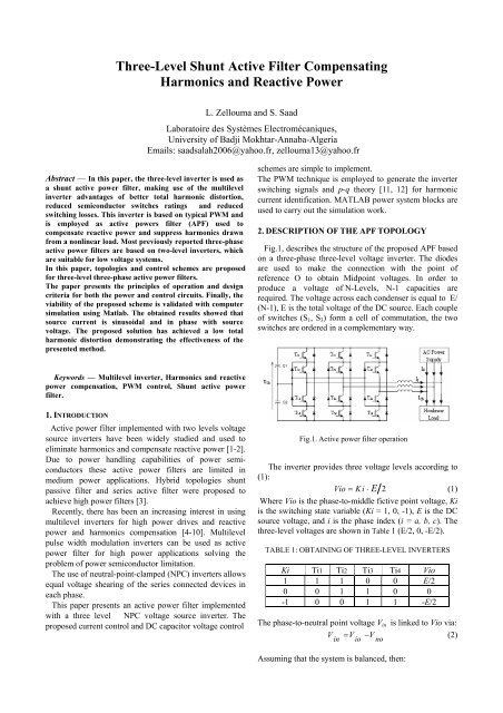
2. DESCRIPTION OF THE APF TOPOLOGY<br />
Fig.1, describes the structure of the proposed APF based<br />
on a three-phase three-level voltage inverter. The diodes<br />
are used to make the connection with the point of<br />
reference O to obtain Midpoint voltages. In order to<br />
produce a voltage of N-<strong>Level</strong>s, N-1 capacities are<br />
required. The voltage across each condenser is equal to E/<br />
(N-1), E is the total voltage of the DC source. Each couple<br />
of switches (S 1 , S 3 ) form a cell of commutation, the two<br />
switches are ordered in a complementary way.<br />
Keywords — Multilevel inverter, <strong>Harmonics</strong> <strong>and</strong> reactive<br />
power compensation, PWM control, <strong>Shunt</strong> active power<br />
filter.<br />
1. INTRODUCTION<br />
<strong>Active</strong> power filter implemented with two levels voltage<br />
source inverters have been widely studied <strong>and</strong> used to<br />
eliminate harmonics <strong>and</strong> compensate reactive power [1-2].<br />
Due to power h<strong>and</strong>ling capabilities of power semiconductors<br />
these active power filters are limited in<br />
medium power applications. Hybrid topologies shunt<br />
passive filter <strong>and</strong> series active filter were proposed to<br />
achieve high power filters [3].<br />
Recently, there has been an increasing interest in using<br />
multilevel inverters for high power drives <strong>and</strong> reactive<br />
power <strong>and</strong> harmonics compensation [4-10]. Multilevel<br />
pulse width modulation inverters can be used as active<br />
power filter for high power applications solving the<br />
problem of power semiconductor limitation.<br />
The use of neutral-point-clamped (NPC) inverters allows<br />
equal voltage shearing of the series connected devices in<br />
each phase.<br />
This paper presents an active power filter implemented<br />
with a three level NPC voltage source inverter. The<br />
proposed current control <strong>and</strong> DC capacitor voltage control<br />
Fig.1. <strong>Active</strong> power filter operation<br />
The inverter provides three voltage levels according to<br />
(1):<br />
Vio = K i ⋅ E 2<br />
(1)<br />
Where Vio is the phase-to-middle fictive point voltage, Ki<br />
is the switching state variable (Ki = 1, 0, -1), E is the DC<br />
source voltage, <strong>and</strong> i is the phase index (i = a, b, c). The<br />
three-level voltages are shown in Table 1 (E/2, 0, -E/2).<br />
TABLE 1: OBTAINING OF THREE-LEVEL INVERTERS<br />
Ki Ti1 Ti2 Ti3 Ti4 Vio<br />
1 1 1 0 0 E/2<br />
0 0 1 1 0 0<br />
-1 0 0 1 1 -E/2<br />
The phase-to-neutral point voltage V in is linked to Vio via:<br />
V = V − V<br />
(2)<br />
in io no<br />
Assuming that the system is balanced, then:
V + V + V = 0<br />
(3)<br />
an bn cn<br />
By substituting (3) in (2), the equation presented below is<br />
obtained:<br />
( )<br />
1<br />
V = V + V + V<br />
(4)<br />
no 3 ao bo co<br />
The expressions of instantaneous inverter phase output<br />
voltages are obtained by replacing (4) in (2):<br />
⎡V<br />
⎤<br />
an ⎡ 2/3 −1/3 −1/3⎤<br />
⎡V<br />
⎤<br />
ao<br />
⎢ ⎥<br />
V = ⎢−1/3 2/3 −1/3⎥<br />
⎢ ⎥<br />
⋅ V<br />
⎢ bn ⎥ bo<br />
⎢<br />
⎥ ⎢ ⎥<br />
⎢V<br />
−1/3 −1/3 2/3<br />
⎣ V<br />
cn<br />
⎥⎦ ⎣<br />
⎦ ⎢⎣ co<br />
⎥⎦<br />
The line to line voltages are determined by the following<br />
equation:<br />
⎡V<br />
⎤<br />
ab ⎡ 1 −1 0⎤<br />
⎡V<br />
⎤<br />
ao<br />
⎢ ⎥<br />
V = ⎢ 0 1 −1⎥<br />
⎢ ⎥<br />
⋅ V<br />
⎢ bc ⎥ ⎢ ⎥ ⎢ bo ⎥<br />
⎢V<br />
−1 0 1<br />
⎣ V<br />
ca<br />
⎥⎦ ⎣ ⎦ ⎢⎣ co<br />
⎥⎦<br />
3. REFERENCE CURRENT CALCULATION<br />
Several methods were proposed for the identification of<br />
the harmonic current references. Mainly, the methods<br />
based on the FFT (Fast Fourier Transformation) in the<br />
frequency domain <strong>and</strong> the methods based on instantaneous<br />
power calculation in the time domain. In this study, the p-<br />
q theory method is used allowing the compensation of<br />
harmonic currents, reactive power <strong>and</strong> unbalanced<br />
currents.<br />
The reference currents (harmonic currents)<br />
identification is based on α-β transformation to obtain real<br />
<strong>and</strong> imaginary powers.<br />
The voltages (V S1 , V S2 , V S3 ) <strong>and</strong> currents (I S1 , I S2 , I S3 )<br />
are transformed to bi-phase system according to the<br />
following equation:<br />
X<br />
⎡ 1 1 ⎤<br />
1<br />
⎡ X<br />
⎢ − −<br />
⎥ ⎤<br />
1<br />
⎡ α ⎤ 2 2 2 ⎢<br />
X<br />
⎥<br />
⎢ 2<br />
X<br />
⎥=<br />
⎢<br />
⎥<br />
β 3 3 3<br />
⎢ ⎥<br />
⎣ ⎦ ⎢<br />
⎥<br />
0<br />
⎢X<br />
⎥<br />
3<br />
⎢<br />
⎣<br />
−<br />
2 2<br />
⎥<br />
⎦<br />
⎣ ⎦<br />
The instantaneous active <strong>and</strong> reactive powers of the<br />
system are calculated as follows:<br />
p<br />
⎛V<br />
V ⎞⎡I<br />
⎤<br />
⎡ ⎤ sα<br />
sβ<br />
α<br />
⎢<br />
q<br />
⎥ = ⎜<br />
−Vsβ V<br />
⎟⎢<br />
sα I<br />
⎥<br />
β<br />
⎣ ⎦ ⎝ ⎠⎣ ⎦<br />
(5)<br />
(6)<br />
(7)<br />
(8)<br />
Instantaneous powers are composed from a constant<br />
part <strong>and</strong> a variable part corresponding to fundamental <strong>and</strong><br />
harmonic currents respectively.<br />
⎡Ihα<br />
⎤ 1 ⎡Vsα −Vsβ⎤⎡p%<br />
⎤<br />
⎢ 2 2<br />
I<br />
⎥ =<br />
h β Vsα<br />
+ V<br />
⎢<br />
sβ<br />
Vsβ V<br />
⎥⎢<br />
sα<br />
q<br />
⎥<br />
⎣ ⎦ ⎣ ⎦⎣%<br />
⎦<br />
4. HARMONIC CURRENTS CONTROL USING<br />
PWM<br />
(9)<br />
This control implements initially a proportional<br />
controller which starts from the difference between the<br />
injected current (active filter current) <strong>and</strong> reference current<br />
(identified current) that determines the reference voltage<br />
of the inverter (modulating wave). This st<strong>and</strong>ard reference<br />
voltage is compared with two carrying triangular identical<br />
waves shifted one from other by a half period of chopping.<br />
The control of inverter arm constituting the filter is<br />
summarized in the two following stages.<br />
• Determination of the intermediate signals V i1 <strong>and</strong> V i2 .<br />
If error ≥ carrying 1 => V i1 = 1<br />
If error < carrying 1 => V i1 = 0<br />
If error ≥ carrying 2 => V i2 = 0<br />
If error < carrying 2 => V i2 =-1<br />
• Determination of control signals of the switches Tij (j<br />
= 1, 2, 3, 4).<br />
If (V i1 + V i2 ) = 1 => T i1 = 1, T i2 = 1, T i3 = 0, T i4 = 0<br />
If (V i1 + V i2 ) = 0 => T i1 = 0, T i2 = 1, T i3 = 1, T i4 = 0<br />
If (V i1 + V i2 ) = -1 => T i1 = 0, T i2 = 0, T i3 = 1, T i4 = 1<br />
The general block diagram of control currents is<br />
illustrated in Fig.2.<br />
Fig.2. PWM synoptic block diagram of currents control<br />
5. DC CAPACITOR VOLTAGE CONTROL<br />
The capacitors (C1<strong>and</strong> C2) average voltage (Vdc1, Vdc2)<br />
has to be maintained at a fixed value. The main cause of<br />
its variation is the active filter switching losses <strong>and</strong> output<br />
filter.<br />
To ensure inverter permanent <strong>and</strong> continuous voltage<br />
supply, a controlled scheme is adopted as illustrated in<br />
Fig.3.
Fig.3. Dc voltage control block.<br />
6. SIMULATION<br />
The simulation is carried out using a program working<br />
in MATLAB Simulink environment. The simulation<br />
parameters are shown in table.2, presented below.<br />
Fig. 5. APF output voltage Vao.<br />
TABLE 2: SIMULATION PARAMETERS<br />
Supply: Vs, Rs, Ls<br />
DC Load: RDC, LDC<br />
<strong>Active</strong> <strong>Filter</strong>: E, Lf, C1,C2<br />
Iref Calculation : fo<br />
Switching frequency<br />
220 V, 0.01Ω, 0.1 mH.<br />
0.5Ω, 0.3 mH.<br />
1000 V, 0.2mH,3μF, 3μF<br />
65 HZ<br />
10 K HZ<br />
The obtained switching signals of the three-phase threelevel<br />
inverter are shown in the Fig.4.<br />
Fig. 6. APF output voltage Van.<br />
Fig. 7. <strong>Active</strong> filter current If.<br />
Fig. 4. Switching pulses of APF arm<br />
(S11, S12, S13, , S14)
Fig. 11. Supply current Is waveform after filtering<br />
Fig. 8. DC voltage of the condensers<br />
(Vdc1, Vdc2 <strong>and</strong> Total Vdc)<br />
Fig. 12. Source current spectrum with filter<br />
The load current obtained by simulation before the use of<br />
active filter is illustrated in Fig.9. This current is highly<br />
distorted <strong>and</strong> its THD calculated from the frequency<br />
spectrum shown in Fig.10 is equal to 15.66%.<br />
Fig.13. Power factor correction (Vs, Is)<br />
Fig. 9. Supply current Is waveform before filtering<br />
Fig. 10. Source current spectrum without filter<br />
7. RESULTS AND DISCUSSIONS<br />
<strong>Three</strong>-level shunt active power filter performances are<br />
related to current references quality, p-q theory is used for<br />
harmonic currents identification <strong>and</strong> calculation the<br />
obtained current is shown in Fig.7. This method is very<br />
important; it allows harmonic currents <strong>and</strong> reactive power<br />
compensation simultaneously, the obtained current <strong>and</strong><br />
voltage waveforms are in phase as illustrated in Fig.13.<br />
Fig.8 shows the results of the DC voltage Vdc1 <strong>and</strong> Vdc2<br />
across the capacitors C1 <strong>and</strong> C2 controlled by P controller,<br />
the obtained total Vdc voltage in constant showing the<br />
efficiency of the controlled scheme.<br />
Compared with the st<strong>and</strong>ard two-level inverter voltage<br />
waveform, from Fig.6 it can be concluded that the threelevel<br />
inverter contains less harmonic contents. The three<br />
level voltages are: 333.33 V, 500 V, <strong>and</strong> 666.66 V,<br />
corresponding respectively to Vdc/3, Vdc/2, <strong>and</strong> 2 Vdc/3,<br />
the DC voltage source (Vdc) is 1000V.
The three level active filter has imposed a sinusoidal<br />
source current waveform instantaneously as illustrated in<br />
Fig.11. The current THD is reduced from 15.66% to 1.3%<br />
as shown in the frequency current spectrum of Fig.11 <strong>and</strong><br />
12, respectively.<br />
CONCLUSION<br />
A theoretical study with simulatin of three-level shunt<br />
active power filter controlled with the PWM modulation<br />
was presented <strong>and</strong> analysed in this paper. The threelevel<br />
APF provides numerous advantages such as<br />
improvement of the supply current wave form, less<br />
harmonic distortion <strong>and</strong> its use in high power/medium<br />
voltage with a lower maximum device rating. The<br />
effectiveness of the proposed scheme is proved by<br />
simulation using MATLAB.<br />
REFERENCES<br />
[1] H. Akagi, “Utility applications of power electronics”<br />
in Conf. Proceedings of IPEC Yokohama 95, pp 19-22,<br />
1995.<br />
[2] H. Akagi, “Trend in <strong>Active</strong> Power Line Conditioners”,<br />
in IEEE Trans. On Ind. Electronics, Vol.9, N°3, pp. 263-<br />
268, August 1994.<br />
[3] Adel M. Al-Zamel <strong>and</strong> David A. Torrey “A three<br />
phase hybrid series passive/shunt active filter system”<br />
IEEE transactions on power electronics, pp.875-<br />
881,1999.<br />
[4] H. Akagi, A. Nabae, “Control strategy of active power<br />
filters using multiple voltage source PWM converters”,<br />
IEEE Trans. Ind. Appl. IA-22 (May/June), pp.460–465.<br />
1986<br />
[5] A. Nabae, I. Takahashi, H. Akagi, “A new neutralpoint-clamped<br />
PWM inverter”, IEEE Trans. Ind. Appl. 17<br />
September (5), pp. 518–523, 1981.<br />
[6] V. Aburto, M. Schneider, L. Moran, J.An. Dixon,<br />
“active power filter implemented with a three-level NPC<br />
voltage-source inverter”, IEEE Power Electronics<br />
Specialists Conference, pp.1121 – 1126, Jun 1997.<br />
[7] Jin. Taotao, Wen. Jun, K. Smedley, “Control <strong>and</strong><br />
topologies for three-phase three-level active power<br />
filters”, IEEE Applied Power Electronics Conference <strong>and</strong><br />
Exposition, pp. 655 – 664, March 2005.<br />
[8] A.M. Massoud, S.J inney, D.M. Grant, B.W.<br />
Williams, “Predictive Current Controlled <strong>Shunt</strong> <strong>Active</strong><br />
Power <strong>Filter</strong> Using <strong>Three</strong>-level Cascaded Type Inverter”,<br />
IEEE IET International Conference, pp.388 – 393, March<br />
2006.<br />
[9] B.-R. Lin, T.-Y. Yang, “<strong>Three</strong>-level voltage-source<br />
inverter for shunt active filter”, IEE, Electric Power<br />
Applications,pp.744–751,Nov.2004.<br />
[10] B.-R. Lin, H. K. Chiang, C.-H. Huang, “<strong>Three</strong>-phase<br />
three-level active power filter with a clamped capacitor<br />
topology”, IEE, Electric Power Applications, pp.513 –<br />
522, July 2006.<br />
[11] H. Akagi, Y. Kanazawa, A. Nabae, “Generalized<br />
theory of the instantaneous reactive power in three-phase<br />
circuits”, In proceedings of the 1985 international power<br />
electronics conference, Tokyo, Japan, pp.1375-1386,<br />
1983.<br />
[12] M. Gaiceau, “<strong>Active</strong> power compensator of the<br />
current harmonics based on the instantaneous power<br />
theory”, The annals of “dunarea de jos” University of<br />
Galati FASCLE III. ISSN 1221-454X, pp.23-28, 2005.