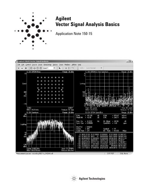
Agilent Vector Signal Analysis Basics - Agilent Technologies
Agilent Vector Signal Analysis Basics - Agilent Technologies
Agilent Vector Signal Analysis Basics - Agilent Technologies

Create successful ePaper yourself
Turn your PDF publications into a flip-book with our unique Google optimized e-Paper software.
<strong>Agilent</strong><br />
<strong>Vector</strong> <strong>Signal</strong> <strong>Analysis</strong> <strong>Basics</strong><br />
Application Note 150-15
Chapter 1<br />
<strong>Vector</strong> <strong>Signal</strong> Analyzer<br />
This application note serves as a primer on the vector signal analyzer (VSA).<br />
This chapter discusses VSA measurement concepts and theory of operation;<br />
Chapter 2 discusses VSA vector-modulation analysis and, specifically,<br />
digital-modulation analysis.<br />
Analog, swept-tuned spectrum analyzers use superheterodyne technology<br />
to cover wide frequency ranges; from audio, through microwave, to millimeter<br />
frequencies. Fast Fourier transform (FFT) analyzers use digital signal<br />
processing (DSP) to provide high-resolution spectrum and network analysis,<br />
but are limited to low frequencies due to the limits of analog-to-digital<br />
conversion (ADC) and signal processing technologies. Today’s wide-bandwidth,<br />
vector-modulated (also called complex or digitally modulated), time-varying<br />
signals benefit greatly from the capabilities of FFT analysis and other DSP<br />
techniques. VSAs combine superheterodyne technology with high speed<br />
ADCs and other DSP technologies to offer fast, high-resolution spectrum<br />
measurements, demodulation, and advanced time-domain analysis.<br />
A VSA is especially useful for characterizing complex signals such as<br />
burst, transient, or modulated signals used in communications, video,<br />
broadcast, sonar, and ultrasound imaging applications.<br />
Figure 1-1 shows a simplified block diagram of a VSA analyzer. The VSA<br />
implements a very different measurement approach than traditional<br />
swept analyzers; the analog IF section is replaced by a digital IF section<br />
incorporating FFT technology and digital signal processing. The traditional<br />
swept-tuned spectrum analyzer is an analog system; the VSA is fundamentally<br />
a digital system that uses digital data and mathematical algorithms to<br />
perform data analysis. For example, most traditional hardware functions,<br />
such as mixing, filtering, and demodulation, are accomplished digitally,<br />
as are many measurement operations. The FFT algorithm is used for<br />
spectrum analysis, and the demodulator algorithms are used for vector<br />
analysis applications.<br />
Analog data<br />
Digitized data stream<br />
t<br />
t<br />
FFT<br />
RF<br />
input<br />
Local<br />
oscilator<br />
IF<br />
input<br />
ADC<br />
LO<br />
90 degs<br />
Anti-alias<br />
filter Quadrature<br />
detector,<br />
digital filtering<br />
Digital IF<br />
and<br />
DSP techniques<br />
Time<br />
Demodulator<br />
Time domain<br />
t<br />
f<br />
Frequency domain<br />
Q<br />
I<br />
Modulation domain<br />
I<br />
Q<br />
0 code 15<br />
Code domain<br />
Figure 1-1. The vector signal analyzer digitizes the analog input signal and uses DSP technology<br />
to process and provide data outputs; the FFT algorithm produces frequency domain results,<br />
the demodulator algorithms produce modulation and code domain results<br />
2
A significant characteristic of the VSA is that it is designed to measure and<br />
manipulate complex data. In fact, it is called a vector signal analyzer because<br />
it has the ability to vector detect an input signal (measure the magnitude<br />
and phase of the input signal). You will learn about vector modulation and<br />
detection in Chapter 2. It is basically a measurement receiver with system<br />
architecture that is analogous to, but not identical to, a digital communications<br />
receiver. Though similar to an FFT analyzer, VSAs cover RF and microwave<br />
ranges, plus additional modulation-domain analysis capability. These<br />
advancements are made possible through digital technologies such as<br />
analog-to-digital conversion and DSP that include digital intermediate<br />
frequency (IF) techniques and fast Fourier transform (FFT) analysis.<br />
Because the signals that people must analyze are growing more complex, the<br />
latest generations of spectrum analyzers have moved to a digital architecture<br />
and often include many of the vector signal analysis capabilities previously<br />
found only in VSAs. Some analyzers digitize the signal at the instrument<br />
input, after some amplification, or after one or more downconverter stages.<br />
In any of these cases, phase as well as magnitude is preserved in order to<br />
perform true vector measurements. Capabilities are then determined by<br />
the digital signal processing capability inherent in the spectrum analyzer<br />
firmware or available as add-on software running either internally<br />
(measurement personalities) or externally (vector signal analysis software)<br />
on a computer connected to the analyzer.<br />
VSA measurement advantages<br />
<strong>Vector</strong> analysis measures dynamic signals and produces complex data results<br />
The VSA offers some distinct advantages over analog swept-tuned analysis.<br />
One of the major advantages of the VSA is its ability to better measure<br />
dynamic signals. Dynamic signals generally fall into one of two categories:<br />
time-varying or complex modulated. Time-varying are signals whose<br />
measured properties change during a measurement sweep (such as burst,<br />
gated, pulsed, or transient). Complex-modulated signals cannot be solely<br />
described in terms of simple AM, FM, or PM modulation, and include most<br />
of those used in digital communications, such as quadrature amplitude<br />
modulation (QAM).<br />
Swept analysis<br />
<strong>Vector</strong> analysis<br />
Time domain<br />
Fourier analysis<br />
Frequency domain<br />
Frequency<br />
resolution<br />
bandwidth<br />
IF filter<br />
A<br />
Start frequency<br />
Carrier<br />
Sweep span<br />
f<br />
Stop frequency<br />
0<br />
Time sampled data<br />
Time record<br />
t<br />
A<br />
Simulated parallel-filter processing<br />
f 1 f 2<br />
Frequency spectrum<br />
Display shows full<br />
spectral display<br />
f<br />
Figure 1-2. Swept-tuned analysis displays the instantaneous time response of a narrowband IF filter<br />
to the input signal. <strong>Vector</strong> analysis uses FFT analysis to transform a set of time domain samples into<br />
frequency domain spectra.<br />
3
A traditional swept-spectrum analyzer 1 , in effect, sweeps a narrowband<br />
filter across a range of frequencies, sequentially measuring one frequency at<br />
a time. Unfortunately, sweeping the input works well for stable or repetitive<br />
signals, but will not accurately represent signals that change during the<br />
sweep. Also, this technique only provides scalar (magnitude only) information,<br />
though some other signal characteristics can be derived by further analysis<br />
of spectrum measurements.<br />
The VSA measurement process simulates a parallel bank of filters and<br />
overcomes swept limitations by taking a “snapshot,” or time-record, of the<br />
signal; then processing all frequencies simultaneously. For example, if the<br />
input is a transient signal, the entire signal event is captured (meaning all<br />
aspects of the signal at that moment in time are digitized and captured);<br />
then used by the FFT to compute the “instantaneous” complex spectra<br />
versus frequency. This process can be performed in real-time, that is, without<br />
missing any part of the input signal. For these reasons, the VSA is sometimes<br />
referred to as a “dynamic signal analyzer” or a “real-time signal analyzer”.<br />
The VSA’s ability to track a fast-changing signal isn’t unlimited, however; it<br />
depends on the VSA’s computational capability.<br />
The VSA decreases measurement time<br />
Parallel processing yields another potential advantage for high-resolution<br />
(narrow resolution bandwidth) measurements; faster measurement time.<br />
If you’ve used a swept-tuned spectrum analyzer before, you already know<br />
that narrow resolution bandwidth (RBW) measurements of small frequency<br />
spans can be very time-consuming. Swept-tuned analyzers sweep frequencies<br />
from point to point slowly enough to allow the analog resolution bandwidth<br />
filters to settle. By contrast, the VSA measures across the entire frequency<br />
span at one time. However, there is analogous VSA settling time due to the<br />
digital filters and DSP. This means the VSA sweep speed is limited by data<br />
collection and digital processing time rather than analog filters. But this<br />
time is usually negligible when compared to the settling time of analog<br />
filters. For certain narrow bandwidth measurements, the VSA can complete<br />
a measurement up to 1000 times faster than conventional swept-tuned<br />
analyzers.<br />
In a swept-tuned spectrum analyzer, the physical bandwidth of the sweeping<br />
filter limits the frequency resolution. The VSA doesn’t have this limitation.<br />
Some VSAs can resolve signals that are spaced less than 100 µHz apart.<br />
Typically, VSA resolution is limited by source and analyzer frequency<br />
stability, as well as by the amount of time you are willing to devote to the<br />
measurement. Increasing the resolution also increases the time it takes to<br />
measure the signal (the length of the required time-record).<br />
Time-capture is a great tool for signal analysis and troubleshooting<br />
Another feature that is extremely useful is the time-capture capability.<br />
This allows you to record actual signals in their entirety without gaps, and<br />
replay them later for any type of data analysis. The full set of measurement<br />
features can be applied to the captured signal. For example, you could<br />
capture a transmitted digital communications signal and then perform<br />
both spectrum and vector-modulation analysis to measure signal quality<br />
or identify signal impairments.<br />
1. For more information on spectrum analyzers, see<br />
<strong>Agilent</strong> Application Note 150, Spectrum <strong>Analysis</strong><br />
<strong>Basics</strong>, literature number 5952-0292.<br />
4
DSP provides multi-domain measurements in one instrument<br />
The use of digital signal processing (DSP) also yields additional benefits;<br />
it provides time, frequency, modulation, and code domain measurement<br />
analysis in one instrument. Having these capabilities increases the analyzer’s<br />
value to you and improves the quality of your measurements. FFT analysis<br />
allows easy and accurate views of both time and frequency domain data.<br />
The DSP provides vector modulation analysis, including both analog and<br />
digital modulation analysis. The analog demodulator produces AM, FM<br />
and PM demodulation results, similar to that of a modulation analyzer,<br />
allowing you to view amplitude, frequency, and phase profiles versus time.<br />
The digital demodulator performs a broad range of measurements on many<br />
digital communications standards (such as W-CDMA, GSM, cdma2000, and<br />
more) and produces many useful measurement displays and signal-quality<br />
data.<br />
Although the VSA clearly provides important benefits, the conventional<br />
analog swept-tuned analyzers can provide higher frequency coverage and<br />
increased dynamic range capability.<br />
VSA measurement concepts and theory of operation<br />
As mentioned earlier, the VSA is fundamentally a digital system that<br />
uses DSP to perform spectrum analysis with FFTs, and uses demodulator<br />
algorithms to perform vector-modulation analysis. You may recall from<br />
Fourier analysis, that the FFT is a mathematical algorithm that operates on<br />
time-sampled data and provides time-to-frequency domain transformations.<br />
The analog signal must be digitized in the time-domain, then the FFT<br />
algorithm executes to compute the spectra. Conceptually, the VSA<br />
implementation is simple and straightforward: digitize the input signal,<br />
then compute the measurement results. See Figure 1-3. However, in<br />
practice, there are many factors that must be accounted for in order for<br />
the measurement to be meaningful and accurate. (For more information<br />
about FFT analysis, refer to the References section at the end of this<br />
application note.)<br />
1 kHz sine wave Digitzed 1kHz sine wave<br />
t<br />
.<br />
.<br />
.<br />
.<br />
. ..<br />
.<br />
.<br />
.<br />
.<br />
.<br />
.<br />
.<br />
.<br />
. .<br />
. .<br />
.<br />
.<br />
ADC .<br />
.<br />
.<br />
.<br />
. .<br />
.<br />
. FFT<br />
t<br />
. .<br />
Sampler and<br />
A/D converter<br />
Time record<br />
Fast Fourier transform<br />
(FFT) processing<br />
1 kHz spectrum<br />
f<br />
1 kHz<br />
Frequency spectrum<br />
Figure 1-3. 1 kHz FFT analysis example: digitize time-domain signal and use FFT analysis to convert<br />
it to the frequency domain<br />
5
If you are familiar with FFT analysis, you already know the FFT algorithm<br />
makes several assumptions about the signal it is processing. The algorithm<br />
doesn’t check to verify the validity of these assumptions for a given input,<br />
and it will produce invalid results, unless you or the instrument validates<br />
the assumptions. Fortunately, as you will learn in the following discussion,<br />
the <strong>Agilent</strong> VSA implementation was designed with FFT-based analysis in<br />
mind. It has many integrated features to eliminate potential error sources,<br />
plus enhancements that provide swept-tuned usability in an FFT-based<br />
analyzer.<br />
Figure 1-4 illustrates a general system block diagram of a VSA analyzer.<br />
Different manufacturers might use slightly different designs and, through<br />
DSP, many of the functions could occur at different places. Figure 1-4 shows<br />
a generalized diagram of the technique that <strong>Agilent</strong> uses in its VSAs. The<br />
VSA spectrum analysis measurement process includes these fundamental<br />
stages:<br />
1. <strong>Signal</strong> conditioning with frequency translation<br />
2. Analog-to-digital conversion<br />
3. Quadrature detection<br />
4. Digital filtering and resampling<br />
5. Data windowing<br />
6. FFT analysis (for vector modulation, blocks 5 and 6 are replaced<br />
with the demodulator block)<br />
The first stage of the measurement process is called signal conditioning.<br />
This stage includes several important functions that condition and optimize<br />
the signal for the analog-to-digital conversion and FFT analysis. The first<br />
function is AC and DC coupling. This option is necessary if you need to<br />
remove unwanted DC biases in the measurement setup. Next, the signal is<br />
either amplified or attenuated for optimal signal level into the mixer. The<br />
mixer stage provides frequency translation, or RF-to-IF downconversion,<br />
and mixes the signal down to the final IF. This operation is the same as<br />
the superheterodyne function of the swept-tuned analyzer and extends<br />
FFT analysis capabilities through microwave. In practice, it may take several<br />
downconversion stages to reach the final IF frequency. Some analyzers<br />
provide external IF input capability; by providing your own IF, you can<br />
extend the upper frequency range of the analyzer to match a receiver<br />
you provide.<br />
1 2 3 4 5 6<br />
RF<br />
input<br />
Attenuation<br />
AC/DC coupling<br />
gain amplifiers<br />
Local<br />
oscilator<br />
Mixer<br />
IF<br />
<strong>Signal</strong> conditioning<br />
Note: Actual VSA implementation<br />
may be different.<br />
IF<br />
ADC<br />
Anti-alias<br />
filter Quadrature<br />
detector<br />
Hardware<br />
implementation<br />
90 degs<br />
Digital<br />
LO<br />
DSP<br />
techniques<br />
I<br />
Q<br />
Digital<br />
decimating<br />
filters<br />
Sampled time<br />
data<br />
Sample<br />
memory<br />
Resampling<br />
(arbitary spans)<br />
Time data<br />
corrections<br />
Time-domain<br />
Window<br />
Demodulator<br />
Display<br />
FFT<br />
"Spectrum analysis"<br />
"<strong>Vector</strong> modulation<br />
analysis"<br />
Code-domain<br />
Modulation-domain<br />
Freq-domain<br />
Figure 1-4. <strong>Vector</strong> signal analyzer simplified block diagram<br />
6
The final stage of the signal conditioning process is extremely important to a<br />
sampled system and FFT analysis; signal alias protection. The anti-alias filter<br />
performs this function. An analyzer that does not have adequate protection<br />
from aliasing may show frequency components that are not part of the<br />
original signal. The sampling theorem states that if the signal is sampled<br />
at a rate greater than 2 times the highest significant frequency component<br />
present in the signal, the sampled signal can be reconstructed exactly.<br />
The minimum acceptable sample rate is called the Nyquist rate. Thus,<br />
f s > 2 (f max )<br />
where f s = sample rate<br />
f max = highest frequency component<br />
If the sampling theorem is violated, “aliasing” error products can result.<br />
Therefore, to prevent alias products for a given maximum frequency, there<br />
must not be significant signal energy above 1/2 the sample rate. Figure 1-5<br />
shows a set of sample points, which fit two different waveforms. The<br />
higher-frequency waveform violates the sampling theorem. Unless an<br />
anti-alias filter is used, the two frequencies will be indistinguishable when<br />
processed digitally.<br />
To prevent aliasing, two conditions must be satisfied:<br />
1. The input signal to the digitizer/sampler must be band limited. In other<br />
words, there must exist a maximum frequency (f max ) above which no<br />
frequency components are present.<br />
2. The input signal must be sampled at a rate that satisfies the sampling<br />
theorem.<br />
The solution to the aliasing problem seems simple enough. First you select<br />
the maximum frequency (f max ) that the analyzer will measure, then make<br />
sure the sampling frequency (f s ) is twice that frequency. This step satisfies<br />
condition number 2 and makes sure that the analyzer can accurately measure<br />
the frequencies of interest. Next you insert a low-pass filter (an anti-aliasing<br />
filter) to remove all frequencies above f max , thus ensuring that the<br />
measurement will exclude all frequencies except those you are interested<br />
in. This step satisfies condition number 1 and makes sure the signal is<br />
band limited.<br />
Actual<br />
signal<br />
Reconstructed "alias" signal<br />
Unwanted frequency components are<br />
folded onto the spectrum below cutoff.<br />
X(f)<br />
recovered alias<br />
spectrum follows<br />
dashed line.<br />
ADC sample<br />
points<br />
f s ( f s /2)<br />
0 f f f s f<br />
(a) Aliasing in the time-domain<br />
(b) Aliasing in the frequency-domain<br />
Figure 1-5. Aliasing products occur when the signal is undersampled. Undesirable frequencies<br />
appear under the alias of another (baseband) frequency<br />
7
There are two factors that complicate this simple anti-aliasing solution.<br />
The first, and easiest to address, is that the anti-alias filter has a finite roll<br />
off rate. As shown in figure 1-6, there is a transition band in practical filters<br />
between the passband and stopband. Frequencies within the transition<br />
band could produce alias frequencies. To avoid these alias products, the<br />
filter cutoff must be below the theoretical upper frequency limit of f s divided<br />
by 2. An easy solution to this problem is to oversample (sample above the<br />
Nyquist rate). Make the sampling frequency slightly above 2 times f max so<br />
that it is twice the frequency at which the stopband actually starts, not twice<br />
the frequency you are trying to measure. Many VSA implementations use<br />
a guard band to protect against displaying aliased frequency components.<br />
The FFT computes the spectral components out to 50% of f s (equivalently<br />
f s /2). A guard band, between approximately 40% to 50% of f s (or f s /2.56 to<br />
f s /2), is not displayed because it may be corrupted by alias components.<br />
However, when the analyzer computes the inverse FFT, the signals in the<br />
guard band are used to provide the most accurate time-domain results.<br />
The high-roll-off-rate filter, combined with the guard band, suppresses<br />
potential aliasing components, attenuating them well below the noise floor<br />
of the analyzer.<br />
The second complicating factor in alias protection (limited frequency<br />
resolution) is much harder to solve. First, an anti-alias filter that is designed<br />
for wide frequency spans (high sample rates) is not practical for measuring<br />
small resolution bandwidths for two reasons; it will require a substantial<br />
sample size (memory allocation) and a prohibitively large number of FFT<br />
computations (long measurement times). For example, at a 10 MHz sample<br />
rate, a 10 Hz resolution bandwidth measurement would require more than<br />
a 1 million point FFT, which translates into large memory usage and a long<br />
measurement time. This is unacceptable because the ability to measure<br />
small resolution bandwidths is one of the main advantages of the VSA.<br />
One way of increasing the frequency resolution is by reducing f s , but this is at<br />
the expense of reducing the upper-frequency limit of the FFT and ultimately<br />
the analyzer bandwidth. However, this is still a good approach because it<br />
allows you to have control over the resolution and frequency range of the<br />
analyzer. As the sample rate is lowered, the cut-off frequency of the anti-alias<br />
filter must also be lowered, otherwise aliasing will occur. One possible<br />
solution would be to provide an anti-aliasing filter for every span, or a filter<br />
with selectable cutoff frequencies. Implementing this scheme with analog<br />
filters would be difficult and cost prohibitive, but it is possible to add<br />
additional anti-alias filters digitally through DSP.<br />
Guard band<br />
Wideband<br />
input signal<br />
Passband Transition Stopband<br />
f<br />
( fs / 2.56 ) ( f s / 2 )<br />
Band limited<br />
analog signal<br />
ADC<br />
Anti-alias filter<br />
Figure 1-6. The anti-alias filter attenuates signals above fs/2. A guard band between 40% to 50%<br />
of fs is not displayed<br />
8
Digital decimating filters and resampling algorithms provide the solution<br />
to the limited frequency resolution problem, and it is the solution used<br />
in <strong>Agilent</strong> VSAs. Digital decimating filters and resampling perform the<br />
operations necessary to allow variable spans and resolution bandwidths.<br />
The digital decimating filters simultaneously decrease the sample rate and<br />
limit the bandwidth of the signal (providing alias protection). The sample<br />
rate into the digital filter is f s ; the sample rate out of the filter is f s /n, where<br />
“n” is the decimation factor and an integer value. Similarly, the bandwidth<br />
at the input filter is “BW,” and the bandwidth at the output of the filter<br />
is “BW/n”. Many implementations perform binary decimation (divide-by-2<br />
sample rate reduction), which means that the sample rate is changed by<br />
integer powers of 2, in 1/(2 n ) steps (1/2, 1/4, 1/8...etc). Frequency spans<br />
that result from “divide by 2 n ” are called cardinal spans. Measurements<br />
performed at cardinal spans are typically faster than measurements<br />
performed at arbitrary spans due to reduced DSP operations.<br />
The decimating filters allow the sample rate and span to be changed by<br />
powers of two. To obtain an arbitrary span, the sample rate must be made<br />
infinitely adjustable. This is done by means of a resampling or interpolation<br />
filter, which follows the decimation filters. For more details regarding<br />
resampling and interpolation algorithms, refer to the References section at<br />
the end of this application note.<br />
Even though the digital and resampling filters provide alias protection while<br />
reducing the sample rate, the analog anti-alias filter is still required, since<br />
the digital and resampling filters are, themselves, a sampled system which<br />
must be protected from aliasing. The analog anti-alias filter protects the<br />
analyzer at its widest frequency span with operation at f s . The digital filters<br />
follow the analog filter and provide anti-alias protection for the narrower,<br />
user-specified spans.<br />
The next complication that limits the ability to analyze small resolution<br />
bandwidths is caused by a fundamental property of the FFT algorithm itself;<br />
the FFT is inherently a baseband transform. This means that the frequency<br />
range of the FFT starts from 0 Hz (or DC) and extends to some maximum<br />
frequency, f s divided by 2. This can be a significant limitation in measurement<br />
situations where a small frequency band needs to be analyzed. For example,<br />
if an analyzer has a sample rate of 10 MHz, the frequency range would be<br />
0 Hz to 5 MHz (f s /2). If the number of time samples (N) were 1024, the<br />
frequency resolution would be 9.8 kHz (f s /N). This means that frequencies<br />
closer than 9.8 kHz could not be resolved.<br />
As just mentioned, you can control the frequency span by varying the sample<br />
rate, but the resolution is still limited because the start frequency of the<br />
span is DC. The frequency resolution can be arbitrarily improved, but<br />
at the expense of a reduced maximum frequency. The solution to these<br />
limitations is a process called band selectable analysis, also known as zoom<br />
operation or zoom mode. Zoom operation allows you to reduce the frequency<br />
span while maintaining a constant center frequency. This is very useful<br />
because it allows you to analyze and view small frequency components<br />
away from 0 Hz. Zooming allows you to focus the measurement anywhere<br />
within the analyzers frequency range (Figure 1-7).<br />
9
Zoom operation is a process of digital quadrature mixing, digital filtering,<br />
and decimating/resampling. The frequency span of interest is mixed with a<br />
complex sinusoid at the zoom span center frequency (f z ), which causes that<br />
frequency span to be mixed down to baseband. The signals are filtered and<br />
decimated/resampled for the specified span, all out-of-band frequencies<br />
removed. This is the band-converted signal at IF (or baseband) and is<br />
sometimes referred to as “zoom time” or “IF time”. That is, it is the timedomain<br />
representation of a signal as it would appear in the IF section of<br />
a receiver. Zoom measurements are discussed further in the “Time-domain<br />
display” section near the end of this chapter.<br />
Sample memory<br />
The output of the digital decimating filters represents a bandlimited, digital<br />
version of the analog input signal in time-domain. This digital data stream is<br />
captured in sample memory (Figure 1-4). The sample memory is a circular<br />
FIFO (first in, first out) buffer that collects individual data samples into<br />
blocks of data called time records, to be used by the DSP for further data<br />
processing. The amount of time required to fill the time record is analogous<br />
to the initial settling time in a parallel-filter analyzer. The time data collected<br />
in sample memory is the fundamental data used to produce all measurement<br />
results, whether in the frequency domain, time domain, or modulation domain.<br />
Time domain data corrections<br />
To provide more accurate data results, many VSAs implement time data<br />
correction capability through an equalization filter. In vector analysis, the<br />
accuracy of the time data is very important. Not only is it the basis for all of<br />
the demodulation measurements, but it is also used directly for measurements<br />
such as instantaneous power as a function of time. Correcting the time data<br />
is the last step in creating a nearly ideal bandlimiting signal path. While the<br />
digital filters and resampling algorithms provide for arbitrary bandwidths<br />
(sample rates and spans), the time-domain corrections determine the final<br />
passband characteristic of the signal path. Time-domain corrections would<br />
be unnecessary if the analog and digital signal paths could be made ideal.<br />
Time-domain corrections function as an equalization filter to compensate<br />
for passband imperfections. These imperfections come from many sources.<br />
The IF filters in the RF section, the analog anti-aliasing filter, the decimating<br />
filters, and the resampling filters all contribute to passband ripple and<br />
phase nonlinearities within the selected span.<br />
Broadband time-domain signal<br />
Digital LO frequency spectrum at f z<br />
Time-domain<br />
baseband<br />
Frequency-domain<br />
response<br />
(a)<br />
(b)<br />
0 Hz<br />
f z<br />
f max<br />
t<br />
(d)<br />
(e)<br />
0 Hz<br />
f z<br />
Frequency translated version of the zoom span<br />
–f 0 Hz<br />
start f stop<br />
Band selectable<br />
analysis<br />
(zoom-mode)<br />
(c)<br />
f start<br />
Zoom span<br />
f z<br />
f stop<br />
(Zoom span center frequency)<br />
(f)<br />
f start<br />
Spectrum display<br />
f z<br />
Analyzer display<br />
f stop<br />
Figure 1-7. Band-selectable analysis (or zoom mode): (a) measured broadband signal,<br />
(b) spectrum of the measured signal, (c) selected zoom span and center frequency,<br />
(d) digital LO spectrum (@ zoom center frequency), (e) frequency span mixed down to baseband,<br />
(f) display spectrum annotation is adjusted to show the correct span and center frequency<br />
10
The design of the equalization filter begins by extracting information about<br />
the analog signal path from the self-calibration data based on the instrument’s<br />
configuration. This is the data used to produce the frequency-domain<br />
correction output display. Once the analog correction vector has been<br />
computed, it is modified to include the effects of the decimating and<br />
resampling filters. The final frequency response computations cannot be<br />
performed until after you have selected the span, because that determines<br />
the number of decimating filter stages and resampling ratio. The composite<br />
correction vector serves as the basis for the design of the digital equalization<br />
filter that is applied to the time data.<br />
Data windowing - leakage and resolution bandwidth<br />
The FFT assumes that the signal it is processing is periodic from time record<br />
to time record. However most signals are not periodic in the time record<br />
and a discontinuity between time records will occur. Therefore, this FFT<br />
assumption is not valid for most measurements, so it must be assumed that<br />
a discontinuity exists. If the signal is not periodic in the time record, the<br />
FFT will not estimate the frequency components accurately. The resultant<br />
effect is called leakage and has the affect of spreading the energy from a<br />
single frequency over a broad range of frequencies. Analog swept-tuned<br />
spectrum analyzers will produce similar amplitude and spreading errors<br />
when the sweep speed is too fast for the bandwidth of the filter.<br />
Data windowing is the usual solution to the leakage problem. The FFT is<br />
not the cause of the error; the FFT is generating an “exact” spectrum for the<br />
signal in the time record. It is the non-periodic signal characteristics between<br />
time records that cause the error. Data windowing uses a window function<br />
to modify the time-domain data by forcing it to become periodic in the time<br />
record. In effect, it forces the waveform to zero at both ends of the time<br />
record. This is accomplished by multiplying the time record by a weighted<br />
window function. Windowing distorts the data in the time domain to improve<br />
accuracy in the frequency domain. See Figure 1-8.<br />
Original<br />
signal<br />
Sampled<br />
time record<br />
Window<br />
function<br />
X =<br />
Modified<br />
waveform<br />
Discontinuities in<br />
the time-record<br />
Log<br />
dB<br />
True<br />
spectrum<br />
Spectrum<br />
with leakage<br />
Log<br />
dB<br />
Reduced leakage<br />
spectrum<br />
f<br />
f<br />
Figure 1-8. Window functions reduce the leakage errors in the frequency domain by modifying the<br />
time domain waveform<br />
11
Analyzers automatically select the appropriate window filter based on<br />
assumptions of the user’s priorities, derived from the selected measurement<br />
type. However, if you want to manually change the window type, VSAs<br />
usually have several built-in window types that you can select from. Each<br />
window function, and the associated RBW filter shape, offers particular<br />
advantages and disadvantages. A particular window type may trade off<br />
improved amplitude accuracy and reduced “leakage” at the cost of reduced<br />
frequency resolution. Because each window type produces different<br />
measurement results (just how different depends on the characteristics<br />
of the input signal and how you trigger on it), you should carefully select<br />
a window type appropriate for the measurement you are trying to make.<br />
Table 1-1 summarizes four common window types and their uses.<br />
Table 1-1. Common window types and uses<br />
Window<br />
Uniform (rectangular, boxcar)<br />
Hanning<br />
Gaussian top<br />
Flat top<br />
Common uses<br />
Transient and self-windowing data<br />
General purpose<br />
High dynamic range<br />
High amplitude accuracy<br />
The window filter contributes to the resolution bandwidth<br />
In traditional swept-tuned analyzers, the final IF filter determines the<br />
resolution bandwidth. In the FFT analyzers, the window type determines<br />
the resolution bandwidth filter shape. And the window type, along with the<br />
time-record length, determines the width of the resolution bandwidth filter.<br />
Therefore, for a given window type, a change in resolution bandwidth will<br />
directly affect the time-record length. Conversely, any change to time-record<br />
length will cause a change in resolution bandwidth as shown in the following<br />
formula:<br />
RBW<br />
= normalized ENBW / T<br />
where<br />
ENBW = equivalent noise bandwidth<br />
RBW = resolution bandwidth<br />
T = time-record length<br />
Equivalent noise bandwidth (ENBW) is a figure of merit that compares the<br />
window filter to an ideal, rectangular filter. It is the equivalent bandwidth<br />
of a rectangular filter that passes the same amount (power) of white noise<br />
as the window. Table 1-2 lists the normalized ENBW values for several<br />
window types. To compute the ENBW, divide the normalized ENBW by<br />
the time-record length. For example, a Hanning window with a 0.5 second<br />
time-record length would have an ENBW of 3 Hz (1.5 Hz-s/0.5 s).<br />
Table 1-2. Normalized ENBW values<br />
Window type<br />
Flat Top<br />
Gaussian top<br />
Hanning<br />
Uniform<br />
Normalized ENBW<br />
3.819 Hz-s<br />
2.215 Hz-s<br />
1.500 Hz-s<br />
1.000 Hz-s<br />
12
Fast Fourier transform (FFT) analysis<br />
The signal is now ready for the FFT algorithm, but the way the FFT operates<br />
on the time-sampled data is not an intuitive process. The FFT is a recordoriented<br />
algorithm and operates on sampled data in a special way. Rather<br />
than acting on each data sample as the ADC converts it, the FFT waits<br />
until a number of samples (N) have been obtained (called a time record),<br />
then transforms the complete block. See Figure 1-9. In other words, a<br />
time record N samples long, is the input to the FFT, and the frequency<br />
spectrum N samples long, is the output.<br />
Sampling<br />
ADC<br />
f s<br />
. ∆ t ..<br />
.<br />
.<br />
.<br />
.<br />
.<br />
.<br />
.<br />
. .<br />
.<br />
.<br />
.<br />
. . .<br />
.<br />
.<br />
. .<br />
0 Samples N<br />
0<br />
Time record<br />
T<br />
N/f s<br />
Time<br />
record<br />
Window<br />
Time records<br />
1 2 ...n<br />
FFT<br />
Spectrum display<br />
∆ f<br />
0<br />
Lines (N/2)<br />
0 Frequency range (f s /2)<br />
f s = Sampling frequency N = Number of sample points<br />
n = Number of lines (or bins)<br />
(sampling rate) (*powers of 2)<br />
= (N/2) + 1<br />
t = 1/f s = Sample time<br />
T = Time record length<br />
= N x t = 1/ f<br />
Figure 1-9. Basic FFT relationships<br />
f = Frequency step<br />
= 1/T = f s /N<br />
The speed of the FFT comes from the symmetry or repeated sample values<br />
that fall out of restricting N to powers of 2. A typical record length for FFT<br />
analysis is 1024 (2 10 ) sample points. The frequency spectrum produced by<br />
the FFT is symmetrical about the sample frequency f s /2 (this value is called<br />
the folding frequency, f f ). Thus, the first half of the output record contains<br />
redundant information, so only the second half is retained, sample points<br />
0 thru N/2. This implies that the effective length of the output record is<br />
(N/2) + 1. You must add 1 to N/2 because the FFT includes the zero line,<br />
producing outputs from 0 Hz thru N/2 Hz inclusive. These are complex data<br />
points that contain both magnitude and phase information.<br />
In theory, the output of the FFT algorithm is (N/2) +1 frequency points,<br />
extending from 0 Hz to f f . In practice however, a guard band is used for alias<br />
protection, so not all of these points are normally displayed. As mentioned<br />
earlier, a guard band (between approximately 40% to 50% of f s ) is not<br />
displayed because it may be corrupted by alias components. For example,<br />
for a record length of 2048 samples, which produces 1025 unique complex<br />
frequency points, only 801 may actually be displayed.<br />
13
These frequency domain points are called lines, or bins, and are usually<br />
numbered from 0 to N/2. These bins are equivalent to the individual<br />
filter/detector outputs in a bank-of-filters analyzer. Bin 0 contains the DC<br />
level present in the input signal and is referred to as the DC bin. The bins are<br />
equally spaced in frequency, with the frequency step (∆f ) being the reciprocal<br />
of the measurement time-record length (T). Thus, ∆f = 1/T. The length of the<br />
time record (T) can be determined from the sample rate (f s ) and the number<br />
of sample points (N) in the time record as follows: T = N/f s . The frequency<br />
( f n ) associated with each bin is given by:<br />
f n = nf s /N<br />
where<br />
n is the bin number<br />
The frequency of the last bin contains the highest frequency, f s /2. Therefore,<br />
the frequency range of an FFT is 0 Hz to f s /2. Note that the highest FFT<br />
range is not f max , which is the upper-frequency limit of the analyzer, and<br />
may not be the same as the highest bin frequency.<br />
Real-time bandwidth<br />
Because the FFT analyzer cannot compute a valid frequency-domain<br />
result until at least one time record is acquired, the time-record length<br />
determines how long an initial measurement will take. For example, a 400-line<br />
measurement using a 1 kHz span requires a 400 ms time record; a 3200-line<br />
measurement requires a 3.2 s time record. This amount of data acquisition<br />
time is independent of the processing speed of the analyzer.<br />
After the time record has been captured, processing speed does become an<br />
issue. The amount of time it takes to compute the FFT, format, and display<br />
the data results, determines the processing speed and display update rate.<br />
Processing speed can be important for two reasons. First, higher processing<br />
speeds can translate to decreased overall measurement time. Second, the<br />
ability of an analyzer to measure dynamic signals is a function of the<br />
processing speed. The performance indicator is the real-time bandwidth<br />
(RTBW), which is the maximum frequency span that can be continuously<br />
processed without missing any event in the input signal.<br />
(a) Real time<br />
Digitized<br />
signal<br />
Time<br />
record 1<br />
Time<br />
record 2<br />
Time<br />
record 3<br />
Time<br />
record 4<br />
FFT 1 FFT 2 FFT 3<br />
(b) Not real-time<br />
These sections of the input signal<br />
are not processed<br />
Digitized<br />
signal<br />
Time<br />
record 1<br />
Time<br />
record 2<br />
Time<br />
record 3<br />
Time<br />
record 4<br />
FFT 1 FFT 2 FFT 3<br />
Input<br />
signal<br />
Time<br />
Figure 1-10. (a) Processing is “real-time” when the FFT processing time is ≤ the time-record<br />
length; no data is lost. (b) Input data is missed if the FFT processing time is greater than the<br />
time-record length<br />
14
In the analyzer, RTBW is the frequency span at which the FFT processing<br />
time equals the time-record length. There is no gap between the end of one<br />
time record and the start of the next. See Figure 1-10. For any frequency<br />
spans less than RTBW, no input data is lost. However, if you increase the<br />
span past the real-time bandwidth, the record length becomes shorter than<br />
the FFT processing time. When this occurs, the time records are no longer<br />
contiguous, and some data will be missed.<br />
Time-domain display<br />
The VSA lets you view and analyze time-domain data. The displayed<br />
time-domain data may look similar to an oscilloscope display, but you<br />
need to be aware that the data you’re viewing may be quite different. The<br />
time-domain display shows the time-data just before FFT processing. See<br />
Figure 1-4. Many VSAs provide two measurement modes, baseband and<br />
zoom. Depending on the measurement mode, the time-domain data you<br />
are viewing will be very different.<br />
Baseband mode provides time data similar to what you would view on a<br />
digital oscilloscope. Like the traditional digital signal oscilloscope (DSO),<br />
a VSA provides real-valued time data referenced to 0 time and 0 Hz (DC).<br />
However, the trace may appear distorted on the VSA, especially at high<br />
frequencies. This is because a VSA samples at a rate chosen to optimize FFT<br />
analysis, which, at the highest frequencies may only be 2 or 3 samples per<br />
period; great for the FFT, but not so good for viewing. In contrast, the DSO<br />
is optimized for time-domain analysis and usually oversamples the input. In<br />
addition, a DSO may provide additional signal reconstruction processing that<br />
enable the DSO to display a better time-domain representation of the actual<br />
input signal. Also, at maximum span, some signals (particularly square waves<br />
and transients) may appear to have excess distortion or ringing because of<br />
the abrupt frequency cut-off of the anti-alias filter. In this sense, DSOs are<br />
optimized for sample rate and time-domain viewing, not power accuracy<br />
and dynamic range.<br />
In zoom (or band selectable) mode, which is typically the default mode<br />
for a VSA, you are viewing the time waveform after it has been mixed and<br />
quadrature detected. Specifically, the time data you are viewing is the<br />
product of analog down conversion, IF filtering, digital quadrature mixing,<br />
and digital filtering/resampling, based on the specified center frequency<br />
and span. The result is a band-limited complex waveform that contains<br />
real and imaginary components and, in most cases, it looks different from<br />
what you would see on an oscilloscope display. This may be valuable<br />
information, depending on the intended use. For example, this could be<br />
interpreted as “IF time,” the time-domain signal that would be measured<br />
with an oscilloscope probing the signal in the IF section of a receiver.<br />
The digital LO and quadrature detector perform the zoom measurement<br />
function. In zoomed measurements, the selected frequency span is mixed<br />
down to baseband at the specified center frequency (f center ). To accomplish<br />
this, first the digital LO frequency is assigned the f center value. Then the input<br />
signal is quadrature detected; it is multiplied or mixed with the sine<br />
and cosine (quadrature) of the center frequency of the measurement span.<br />
The result is a complex (real and imaginary) time-domain waveform that is<br />
now referenced to f center , while the phase is still relative to the zero time<br />
trigger. Remember, the products of the mixing process are the sum and<br />
difference frequencies (signal – f center and signal + f center ). So the data<br />
is further processed by the low-pass filters to select only the difference<br />
15
frequencies. If the carrier frequency (f carrier ) is equal to f center , the<br />
modulation results are the positive and negative frequency sidebands centered<br />
about 0 Hz. However, the spectrum displays of the analyzer are annotated to<br />
show the correct center frequency and sideband frequency values.<br />
Figure 1-11 shows a 13.5 MHz sinewave measured in both baseband and<br />
zoom mode. The span for both measurements is 36 MHz and both start at<br />
0 Hz. The number of frequency points is set to 401. The left-hand time trace<br />
shows a sinewave at its true period of approximately 74 ns (1/13.5 MHz).<br />
The right-hand time trace shows a sinewave with a period of 222.2 ns<br />
(1/4.5 MHz). The 4.5 MHz sinewave is the difference between the 18 MHz<br />
VSA center frequency and the 13.5 MHz input signal.<br />
Real<br />
(<strong>Signal</strong> to fc) = (13.5 MHz to 18 MHz) = – 4.5 MHz<br />
13.5 MHz<br />
sinewave<br />
ADC<br />
f sample<br />
Ø<br />
Digital LO = fc<br />
90° phase shift<br />
Imaginary<br />
Quadrature detector<br />
(or Quadrature mixer)<br />
Baseband: reference to 0 Hz<br />
LO = 0 Hz, fc = 18 MHz, span 36 MHz<br />
Real values only<br />
Baseband signal = 13.5 MHz sinewave<br />
Zoom: reference to center frequency fc<br />
LO = 18 MHz, fc = 18 MHz, span 36 MHz<br />
Real and imaginary values<br />
Zoom signal = 4.5 MHz sinewave<br />
Figure 1-11. Baseband and zoom time data<br />
Summary<br />
This chapter presented a primer on the theory of operation and measurement<br />
concepts using a vector signal analyzer (VSA). We went though the<br />
system block diagram and described each function as it related to the<br />
FFT measurement process. You learned that the implementation used by<br />
the VSA is quite different from the conventional analog, swept-tuned analyzer.<br />
The VSA is primarily a digital system incorporating an all-digital IF, DSP,<br />
and FFT analysis. You learned that the VSA is a test and measurement<br />
solution providing time-domain, frequency-domain, modulation-domain<br />
and code-domain signal analysis capabilities.<br />
This chapter described the spectrum analysis capabilities of the VSA,<br />
implemented thorough FFT analysis. The fundamentals of FFT measurement<br />
theory and analysis were presented. The vector analysis measurement<br />
concepts and demodulator block, which include digital and analog modulation<br />
analysis, are described in Chapter 2.<br />
16
Chapter 2<br />
<strong>Vector</strong> Modulation<br />
<strong>Analysis</strong><br />
Introduction<br />
Chapter 1 was a primer on vector signal analyzers (VSA) and discussed<br />
VSA measurement concepts and theory of operation. It also described the<br />
frequency-domain, spectrum analysis measurement capability of the VSA,<br />
implemented through fast Fourier transform (FFT) analysis. This chapter<br />
describes the vector-modulation analysis and digital-modulation analysis<br />
measurement capability of the VSA. Some swept-tuned spectrum analyzers<br />
can also provide digital-modulation analysis by incorporating additional<br />
digital radio personality software. However, VSAs typically provide more<br />
measurement flexibility in terms of modulation formats and demodulator<br />
configuration, and provide a larger set of data results and display traces. The<br />
basic digital-modulation analysis concepts described in this chapter can also<br />
apply to swept-tuned analyzers that have the additional digital-modulation<br />
analysis software.<br />
The real power of the VSA is its ability to measure and analyze vectormodulated<br />
and digitally modulated signals. <strong>Vector</strong>-modulation analysis<br />
means the analyzer can measure complex signals, signals that have a real<br />
and imaginary component. Since digital communications systems use complex<br />
signals (I-Q waveforms), vector-modulation analysis is required to measure<br />
digitally-modulated signals. But vector-modulation analysis is not enough<br />
to measure today’s complicated digitally-modulated signals. You also need<br />
digital-modulation analysis. Digital-modulation analysis is needed to<br />
demodulate the RF modulated carrier signal into its complex components<br />
(the I-Q waveforms) so you can apply vector-modulation analysis. <strong>Vector</strong><br />
modulation analysis provides the numerical and visual tools to help quickly<br />
identify and quantify impairments to the I-Q waveforms. Digital-modulation<br />
analysis is also needed to detect and recover the digital data bits.<br />
Digital demodulation also provides modulation quality measurements. The<br />
technique used in <strong>Agilent</strong> VSAs (described later in this chapter) can expose<br />
very subtle signal variations, which translates into signal quality information<br />
not available from traditional modulation quality measurement methods.<br />
Various display formats and capabilities are used to view the baseband<br />
signal characteristics and analyze modulation quality. The VSA offers<br />
traditional display formats such as I-Q vector, constellation, eye, and trellis<br />
diagrams. The symbol/error summary table shows the actual recovered bits<br />
and valuable error data, such as error vector magnitude (EVM), magnitude<br />
error, phase error, frequency error, rho, and I-Q offset error. Other display<br />
formats, such as magnitude/phase error versus time, magnitude/phase error<br />
versus frequency, or equalization allow you to make frequency response<br />
and group delay measurements or see code-domain results. This is only<br />
a representative list of available display formats and capabilities. Those<br />
available in a VSA are dependent upon analyzer capability and the type of<br />
digital-modulation format being measured.<br />
17
The VSA, with digital modulation provides measurement support for<br />
multiple digital communication standards, such as GSM, EDGE, W-CDMA,<br />
and cdma2000. Measurements are possible on continuous or burst carriers<br />
(such as TDMA), and you can make measurements at baseband, IF, and RF<br />
locations throughout a digital communications system block diagram. There<br />
is no need for external filtering, coherent carrier signals, or symbol clock<br />
timing signals. The general-purpose design of the digital demodulator<br />
in the VSA also allows you to measure non-standard formats, allowing you<br />
to change user-definable digital parameters for customized test and analysis<br />
purposes.<br />
Another important measurement tool that vector-modulation analysis<br />
provides is analog-modulation analysis. For example, the <strong>Agilent</strong> 89600<br />
VSA provides analog-modulation analysis and produces AM, FM, and PM<br />
demodulation results, similar to what a modulation analyzer would produce,<br />
allowing you to view amplitude, frequency, and phase profiles versus time.<br />
These additional analog-demodulation capabilities can be used to troubleshoot<br />
particular problems in a digital communications transmitter. For example,<br />
phase demodulation is often used to troubleshoot instability at a particular<br />
LO frequency.<br />
The remainder of this chapter contains additional concepts to help you<br />
better understand vector-modulation analysis, digital-modulation analysis,<br />
and analog-modulation analysis.<br />
<strong>Vector</strong> modulation and digital modulation overview<br />
Let’s begin our discussion by reviewing vector modulation and digital<br />
modulation. Digital modulation is a term used in radio, satellite, and<br />
terrestrial communications to refer to modulation in which digital states are<br />
represented by the relative phase and/or amplitude of the carrier. Although<br />
we talk about digital modulation, you should remember that the modulation<br />
is not digital, but truly analog. Modulation is the amplitude, frequency, or<br />
phase modification of the carrier in direct proportion to the amplitude of<br />
the modulating (baseband) signal. See Figure 2-1. In digital modulation, it<br />
is the baseband modulating signal, not the modulation process, that is in<br />
digital form.<br />
Amplitude<br />
1 0 1 0<br />
t<br />
Digital data<br />
Digital baseband<br />
modulating signal<br />
Frequency<br />
t<br />
Phase<br />
t<br />
Amplitude & phase<br />
t<br />
Figure 2-1. In digital modulation, the information is contained in the relative phase, frequency, or<br />
amplitude of the carrier<br />
18
Depending on the particular application, digital modulation may modify<br />
amplitude, frequency, and phase simultaneously and separately. This type of<br />
modulation could be accomplished using conventional analog modulation<br />
schemes like amplitude modulation (AM), frequency modulation (FM), or<br />
phase modulation (PM). However, in practical systems, vector modulation<br />
(also called complex or I-Q modulation) is used instead. <strong>Vector</strong> modulation<br />
is a very powerful scheme because it can be used to generate any arbitrary<br />
carrier phase and magnitude. In this scheme, the baseband digital information<br />
is separated into two independent components: the I (In-phase) and Q<br />
(Quadrature) components. These I and Q components are then combined<br />
to form the baseband modulating signal. The most important characteristic<br />
of I and Q components is that they are independent components (orthogonal).<br />
You’ll learn more about I and Q components and why digital systems use<br />
them in the following discussion.<br />
Q - value<br />
(I ,Q ) 1 1<br />
Q (volts)<br />
Magnitude<br />
1<br />
(Q uadrature or<br />
imaginary part)<br />
θ Phase<br />
A discrete point on the I-Q diagram<br />
represents a digital state or symbol location<br />
–1<br />
I - value<br />
0 deg (carrier phase reference)<br />
1<br />
I (volts)<br />
(In-phase or<br />
real part)<br />
Figure 2-2. Digital modulation I-Q diagram<br />
–1<br />
An easy way to understand and view digital modulation is with the I-Q or<br />
vector diagram shown in Figure 2-2. In most digital communication systems,<br />
the frequency of the carrier is fixed so only phase and magnitude need to be<br />
considered. The unmodulated carrier is the phase and frequency reference,<br />
and the modulated signal is interpreted relative to the carrier. The phase and<br />
magnitude can be represented in polar or vector coordinates as a discrete<br />
point in the I-Q plane. See Figure 2-2. I represents the in-phase (phase<br />
reference) component and Q represents the quadrature (90° out of phase)<br />
component. You can also represent this discrete point by vector addition<br />
of a specific magnitude of in-phase carrier with a specific magnitude of<br />
quadrature carrier. This is the principle of I-Q modulation.<br />
19
By forcing the carrier to one of several predetermined positions in the I-Q<br />
plane, you can then transmit encoded information. Each position or state<br />
(or transitions between the states in some systems) represents a certain bit<br />
pattern that can be decoded at the receiver. The mapping of the states or<br />
symbols at each symbol timing instant (when the receiver interprets the<br />
signal) on the I-Q plane is referred to as a constellation diagram. See<br />
Figure 2-3. A symbol represents a grouping of the digital data bits; they<br />
are symbolic of the digital words they represent. The number of bits<br />
contained in each symbol, or bits-per-symbol (bpsym), is determined by<br />
the modulation format. For example, binary phase shift keying (BPSK)<br />
uses 1 bpsym, quadrature phase shift keying (QPSK) uses 2 bpsym, and<br />
8-state phase shift keying (8PSK) uses 3 bpsym. Theoretically, each state<br />
location on the constellation diagram should show as a single point, but<br />
a practical system suffers from various impairments and noise that cause<br />
a spreading of the states (a dispersal of dots around each state). Figure 2-3<br />
shows the constellation or state diagram for a 16 QAM (16-state quadrature<br />
amplitude modulation) format; note that there are 16 possible state locations.<br />
This format takes four bits of serial data and encodes them as single<br />
amplitude/phase states, or symbols. In order to generate this modulation<br />
format, the I and Q carriers each need to take four different levels of<br />
amplitude, depending on the code being transmitted.<br />
Constellation or state diagram<br />
Symbol mapping to IQ voltages<br />
0011<br />
0111<br />
Q (volts)<br />
0010 0001<br />
1<br />
0110 0101<br />
0000<br />
0100<br />
state: 0100<br />
symbol: 1<br />
I = 1 V<br />
Q = 0.5 V<br />
I<br />
1V<br />
0<br />
01 00<br />
serial bit stream<br />
00 01 11 01 00 10<br />
t<br />
–1<br />
1011<br />
1111<br />
0<br />
1010 1001<br />
1110 1101<br />
-1<br />
16 QAM<br />
1<br />
1000<br />
1100<br />
I (volts)<br />
–1V<br />
1V<br />
Q 0<br />
–1V<br />
symbol timing<br />
instants<br />
1 2 3 4<br />
symbols<br />
t<br />
t<br />
Figure 2-3. Each position, or state, in the constellation diagram represents a specific bit pattern<br />
(symbol) and symbol time<br />
In digital modulation, the signal moves among a limited number of<br />
symbols or states. The rate at which the carrier moves between points in<br />
the constellation is called the symbol rate. The more constellation states<br />
that are used, the lower the required symbol rate for a given bit rate. The<br />
symbol rate is important because it tells you the bandwidth required to<br />
transmit the signal. The lower the symbol rate, the less bandwidth required<br />
for transmission. For example, the 16QAM format, mentioned earlier, uses<br />
4 bits per symbol. If the radio transmission rate is 16 Mbps, then the symbol<br />
rate = 16 (Mbps) divided by 4 bits, or 4 MHz. This provides a symbol rate<br />
that is one-fourth the bit rate and a more spectrally efficient transmission<br />
bandwidth (4 MHz versus 16 MHz). For more detailed information about<br />
digital modulation, see the References section at the end of this application<br />
note.<br />
20
I-Q modulator<br />
The device used in digital communications to generate vector modulation<br />
is the I-Q modulator. The I-Q modulator puts the encoded digital I and Q<br />
baseband information onto the carrier. See Figure 2-4. The I-Q modulator<br />
generates signals in terms of I and Q components; fundamentally it is a<br />
hardware (or software) implementation of a rectangular to polar coordinate<br />
conversion.<br />
Rectangular<br />
coordinates<br />
Polar<br />
coordinates<br />
I baseband<br />
(In-phase component)<br />
Local oscillator<br />
(carrier frequency)<br />
90 deg.<br />
phase shift<br />
Σ<br />
Summing<br />
circuits<br />
Composite<br />
output signal<br />
(I-Q modulated carrier)<br />
Q baseband<br />
(Q uadrature component)<br />
Figure 2-4. I-Q modulator<br />
The I-Q modulator receives the I and Q baseband signals as inputs and<br />
mixes them with the same local oscillator (LO). Thus, I and Q are both<br />
upconverted to the RF carrier frequency. The I information amplitude<br />
modulates the carrier producing the in-phase component. The Q information<br />
amplitude modulates a 90-degree (orthogonal) phase shifted version of<br />
the carrier producing the quadrature component. These two orthogonal<br />
modulated carrier signals are summed together producing the composite<br />
I-Q modulated carrier signal. The main advantage of I-Q modulation is the<br />
symmetric ease of combining independent signal components into a single,<br />
composite signal, and later splitting the composite signal into its independent<br />
component parts.<br />
<strong>Signal</strong>s that are separated by 90 degrees are known as being orthogonal to<br />
each other, or in quadrature. The quadrature relationship between I and Q<br />
signals means that these two signals are truly independent. They are two<br />
independent components of the same signal. While changes of the Q input<br />
certainly alter the composite output signal, they do not change the I<br />
component at all. Similarly, changes of the I input have no effect on the<br />
Q signal.<br />
21
I-Q demodulator<br />
As you can see in Figure 2-5, the I-Q demodulator is a mirror image of the<br />
I-Q modulator shown in Figure 2-4. The I-Q demodulator recovers the original<br />
I and Q baseband signals from a composite I-Q modulated input signal.<br />
Polar<br />
coordinates<br />
Rectangular<br />
coordinates<br />
I baseband<br />
(In-phase component)<br />
Composite<br />
input signal<br />
(I-Q modulated carrier)<br />
Power<br />
splitter<br />
90 deg.<br />
phase shift<br />
Local oscillator<br />
(phase locked to the<br />
carrier frequency)<br />
Q baseband<br />
(Q uadrature component)<br />
Figure 2-5. I-Q demodulator (or quadrature detector)<br />
The first step in the demodulation process is to phase-lock the receiver<br />
LO to the transmitter carrier frequency. It is necessary that the receiver<br />
LO be phase-locked to the transmitter carrier (or mixer LO) to correctly<br />
recover the I and Q baseband components. Then, the I-Q modulated carrier<br />
is mixed with both an unshifted LO, and a 90 degree phase-shifted version<br />
of the LO, producing the original I and Q baseband signals or components.<br />
The I-Q demodulation process is fundamentally a polar to rectangular<br />
conversion. Normally, information cannot be plotted in a polar format and<br />
reinterpreted as rectangular values without doing a polar-to-rectangular<br />
conversion. See Figure 2-2. However, this conversion is exactly what is<br />
done by the in-phase and quadrature mixing processes performed by the<br />
I-Q demodulator.<br />
Why use I and Q?<br />
Digital modulation uses I and Q components because it provides a simple,<br />
efficient, and robust modulation method for generating, transmitting, and<br />
recovering digital data. Modulated signals in the I-Q domain provide many<br />
advantages:<br />
1. The I-Q implementation provides a method to create complex signals<br />
(both phase and amplitude change). Instead of using phase modulation,<br />
which is nonlinear and difficult to do well, the I-Q modulator simply<br />
modulates the amplitude of the carrier and its quadrature in a linear<br />
manner. Mixers with wide modulation bandwidths and good linearity are<br />
readily available. To produce a complex modulated signal, you only need<br />
to generate the baseband I and Q components of the signal. One key<br />
advantage of I-Q modulators is that the same modulator can be used to<br />
generate a variety of modulations from digital formats to RF pulses, or<br />
even radar chirps, for example.<br />
2. Demodulating the signal is also straightforward. Using an I-Q demodulator,<br />
it is simple, at least in principle, to recover the baseband signals.<br />
3. Looking at a signal in the I-Q plane often gives good insights about the<br />
signal. Effects like cross talk, data skew, compression, and AM-to-PM<br />
distortion, which are hard to visualize otherwise, are easy to see.<br />
22
Digital RF communication system concepts<br />
Figure 2-6 shows a generic, simplified block diagram of the basic<br />
architecture of a digital RF communications system that uses I-Q modulation.<br />
By understanding the fundamental concepts of this system, the operation<br />
of the VSA with vector modulation analysis may also be understood. In<br />
Figure 2-6, the system blocks enclosed by the dashed box show sections<br />
of the communications transmitter and receiver that can be measured and<br />
analyzed by the VSA with vector modulation analysis.<br />
Transmitter<br />
Voice<br />
input<br />
ADC<br />
Speech<br />
coding<br />
Processing/<br />
compression/<br />
error correction<br />
Symbol<br />
encoder<br />
I<br />
Q<br />
Baseband<br />
filters<br />
I<br />
Q<br />
IQ<br />
modulator<br />
IF LO<br />
DAC<br />
IF<br />
filter<br />
Upconverter<br />
RF LO<br />
Amplifier<br />
Receiver<br />
AGC<br />
Power<br />
control<br />
Down<br />
convert<br />
RF LO<br />
IF<br />
filter<br />
IQ<br />
demodulator<br />
IF LO<br />
I<br />
Q<br />
Baseband<br />
filters<br />
I<br />
Q<br />
Decode<br />
bits<br />
Adaption/<br />
process/<br />
decompress<br />
ADC<br />
Reconstrution<br />
filter<br />
Voice<br />
output<br />
May not represent actual<br />
radio system block diagram<br />
Figure 2-6. Digital RF communication system simplified block diagram<br />
Digital communication transmitter concepts<br />
The communications transmitter begins with speech coding (assuming<br />
voice transmission) which is the process of quantizing the analog signal<br />
and converting it into digital data (digitization). Then, data compression is<br />
applied to minimize the data rate and increase spectral efficiency. Channel<br />
coding and interleaving are common techniques used to improve signal<br />
integrity by minimizing the effects of noise and interference. Extra bits are<br />
often sent for error correction, or as training sequences, for identification<br />
or equalization. These techniques can also make synchronization (finding<br />
the symbol clock) easier for the receiver. The symbol encoder translates<br />
the serial bit stream into the appropriate I and Q baseband signals, each<br />
corresponding to the symbol mapping on the I-Q plane for the specific<br />
system. The symbol clock represents the frequency and exact timing of the<br />
transmission of the individual symbols. At the symbol clock transitions,<br />
the transmitted carrier is at the correct I-Q (or magnitude/phase) value to<br />
represent a specific symbol (a specific point on the constellation). The time<br />
interval between individual symbols is the symbol clock period, the reciprocal<br />
is the symbol clock frequency. The symbol clock phase is correct when the<br />
symbol clock is aligned with the optimum instant to detect the symbols.<br />
23
Once the I and Q baseband signals have been generated, they are filtered<br />
(band limited) to improve spectral efficiency. An unfiltered output of the<br />
digital radio modulator occupies a very wide bandwidth (theoretically,<br />
infinite). This is because the modulator is being driven by baseband I-Q<br />
square waves with fast transitions; fast transitions in the time domain equate<br />
to wide frequency spectra in the frequency domain. This is an unacceptable<br />
condition because it decreases the available spectrum to other users and<br />
causes signal interference to nearby users, called adjacent-channel-power<br />
interference. Baseband filtering solves the problem by limiting the spectrum<br />
and restricting interference with other channels. In effect, the filtering slows<br />
the fast transitions between states, thereby limiting the frequency spectrum.<br />
Filtering is not without tradeoffs, however; filtering also causes degradation<br />
to the signal and data transmission.<br />
The signal degradation is due to reduction of spectral content and the<br />
overshoot and finite ringing caused by the filters time (impulse) response.<br />
By reducing the spectral content, information is lost and it may make<br />
reconstructing the signal difficult, or even impossible, at the receiver. The<br />
ringing response of the filter may last so long so that it affects symbols that<br />
follow, causing intersymbol interference (ISI). ISI is defined as the extraneous<br />
energy from prior and subsequent symbols that interferes with the current<br />
symbol such that the receiver misinterprets the symbol. Thus, selecting the<br />
best filter becomes a design compromise between spectral efficiency and<br />
minimizing ISI. There is a common, special class of filters used in digital<br />
communication design called Nyquist filters. Nyquist filters are an optimal<br />
filter choice because they maximize data rates, minimize ISI, and limit<br />
channel bandwidth requirements. You will learn more about filters later in<br />
this chapter. To improve the overall performance of the system, filtering is<br />
often shared, or split, between the transmitter and the receiver. In that case,<br />
the filters must be as closely matched as possible and correctly implemented,<br />
in both transmitter and receiver, to minimize ISI. Figure 2-6 only shows one<br />
baseband filter, but in reality, there are two; one each for the I and Q channel.<br />
The filtered I and Q baseband signals are inputs to the I-Q modulator. The<br />
LO in the modulator may operate at an intermediate frequency (IF) or<br />
directly at the final radio frequency (RF). The output of the modulator is<br />
the composite of the two orthogonal I and Q signals at the IF (or RF). After<br />
modulation, the signal is upconverted to RF, if needed. Any undesirable<br />
frequencies are filtered out and the signal is applied to the output amplifier<br />
and transmitted.<br />
24
Digital communications receiver concepts<br />
The receiver is essentially an inverse implementation of the transmitter, but<br />
it is more complex to design. The receiver first downconverts the incoming<br />
RF signal to IF, then demodulates it. The ability to demodulate the signal<br />
and recover the original data is often difficult. The transmitted signal is<br />
often corrupted by such factors as atmospheric noise, competing signal<br />
interference, multipath, or fading.<br />
The demodulation process involves these general stages: carrier frequency<br />
recovery (carrier lock), symbol clock recovery (symbol lock), signal<br />
decomposition to I and Q components (I-Q demodulation), I and Q symbol<br />
detection, bit decoding and de-interleaving (decode bits), decompressing<br />
(expansion to original bit stream), and finally, digital to analog conversion<br />
(if required).<br />
The main difference between the transmitter and receiver is the need for<br />
carrier and symbol clock recovery. Both the symbol clock frequency and<br />
phase (or timing) must be correct in the receiver to demodulate the bits<br />
successfully and recover the transmitted information. For example, the<br />
symbol clock could be set to the correct frequency, but at the wrong phase.<br />
That is, if the symbol clock is aligned to the transitions between symbols,<br />
rather than the symbols themselves, demodulation will be unsuccessful.<br />
A difficult task in receiver design is to create carrier and symbol clock<br />
recovery algorithms. Some clock recovery techniques include measuring<br />
the modulation amplitude variations, or in systems with pulsed carriers,<br />
the power turn-on event can be used. This task can also be made easier<br />
when channel coding in the transmitter provides training sequences or<br />
synchronization bits.<br />
25
VSA digital modulation analysis concepts and theory of operation<br />
The VSA can be viewed as a measuring receiver. It is really an I-Q receiver<br />
employing techniques similar to most digital radio receivers for decoding<br />
digital modulations. However, the difference is that the VSA is designed<br />
for high accuracy parametric measurement and display of modulation<br />
characteristics. Moreover, the VSA is a measurement tool that can measure<br />
and analyze almost every aspect of a digital communications transmitter<br />
and receiver system.<br />
RF<br />
input<br />
LO<br />
Analog<br />
IF<br />
Anti-alias<br />
filter<br />
ADC<br />
Note: Actual VSA implementation<br />
may be different.<br />
Digital<br />
IF<br />
90 °<br />
Digital<br />
LO<br />
Quadrature detector,<br />
digital filter<br />
I<br />
Q<br />
IQ baseband<br />
time data<br />
Sample<br />
memory<br />
Re-sampled,<br />
corrected,<br />
time data<br />
Spectrum analysis<br />
FFT<br />
Demodulator<br />
Digital demod<br />
• Analog demod<br />
<strong>Vector</strong> modulation<br />
analysis<br />
Freq-domain<br />
Time-domain<br />
Code-domain<br />
Modulationdomain<br />
Display<br />
Figure 2-7. The VSA demodulator performs vector signal analysis, including digital and analog<br />
modulation analysis<br />
Figure 2-7 shows an <strong>Agilent</strong> 89600 VSA simplified system block diagram.<br />
You may notice that many of the VSA system blocks are analogous to the<br />
digital communication receiver shown in Figure 2-6. The RF input signal is<br />
downconverted, through several stages of superheterodyne mixing, to an<br />
IF that can be accurately digitized by the ADC. This digitized IF is then vector<br />
(quadrature) detected and digitally filtered; downconverted one last time<br />
to an I and Q baseband form (I-Q time data) and stored in RAM. From here,<br />
DSP algorithms demodulate the signal; recover the carrier and symbol clock<br />
and apply reconstructive filtering and decoding (recover the original bits).<br />
With this DSP software implementation, almost any modulation format can<br />
be demodulated.<br />
The VSA implementation is different from a radio receiver. The VSA deals<br />
with the sampled signals on a block basis; the radio receiver processes<br />
data serially, in real time. When you supply the VSA with radio receiver<br />
parameters, the VSA synthesizes the receiver via processing in the DSP.<br />
It provides all the functions of a receiver, down to making analog waveforms.<br />
Because the signal has been virtually digitized, it can be post-processed and<br />
viewed in any of the time, frequency, or modulation domains.<br />
26
VSA digital demodulator<br />
The heart of the digital demodulation process in the VSA is the digital<br />
demodulator. Figure 2-8 shows a simplified block diagram of the digital<br />
demodulator implementation used in the <strong>Agilent</strong> 89600 VSA. The digital<br />
demodulator is a general purpose demodulator that only requires a minimum<br />
of prior information about the input signal to perform demodulation, and<br />
can be used on a wide variety of modulation formats. The demodulator<br />
provides carrier lock, symbol clock recovery, and bit recovery (decodes the<br />
actual encoded 1s and 0s), and produces the I-Q measured waveforms. The<br />
demodulator also produces ideal I-Q waveforms that are synthesized from<br />
the actual recovered bits (called I-Q reference waveforms). The I-Q measured<br />
and I-Q reference waveforms are subtracted to produce I-Q error waveforms.<br />
The I-Q error waveforms are analyzed to generate the modulation quality<br />
data results, which can be viewed in various data formats and display outputs.<br />
Search<br />
length<br />
Pulse<br />
detection<br />
Freq error<br />
(shown in symbol table)<br />
Baseband<br />
filtering<br />
Result length<br />
I-Q<br />
time data<br />
BW<br />
filter<br />
Carrier and<br />
symbol lock<br />
Compensation<br />
Meas<br />
filter<br />
IQ meas time<br />
Span<br />
Center freq<br />
Amp<br />
droop<br />
I/Q<br />
offset<br />
α/BT<br />
Clock adjust<br />
Symbol rate<br />
Pts per sym<br />
Symbol<br />
timing<br />
recovery<br />
Symbol<br />
detector<br />
Reference<br />
generator<br />
Ref<br />
filter<br />
IQ ref time<br />
Symbol bits<br />
(shown in symbol table)<br />
IQ meas time<br />
Sync word<br />
Sync position<br />
Sync<br />
detector<br />
Error<br />
calc<br />
IQ mag error<br />
IQ phase error<br />
Error vector time/spectrum<br />
Oval items require user input<br />
for demodulator configuration.<br />
Rounded rectangular items are<br />
user adjustable inputs.<br />
IQ meas time<br />
IQ ref time<br />
–<br />
Σ<br />
+<br />
EVM<br />
Mag error<br />
Phase error<br />
I/Q offset<br />
Amp droop<br />
Shown in<br />
symbol table<br />
SNR (QAM only)<br />
Figure 2-8. Digital demodulator block diagram<br />
The demodulation process begins by configuring the demodulator. The<br />
demodulator must be configured to the specific digital modulation format<br />
to properly demodulate and analyze the signal. Most analyzers provide a set<br />
of standard presets, such as GSM, W-CDMA, cdma2000, or 802.11a/b/g,<br />
that automatically configure the demodulator for you. In those cases, you<br />
enter the center frequency, select a standard preset, and the analyzer can<br />
demodulate the signal. Some VSAs, like the <strong>Agilent</strong> 89600 VSA, give you<br />
additional capabilities through a general purpose, user-definable demodulator.<br />
This allows you to customize the demodulator configuration for non-standard<br />
formats or troubleshooting purposes. The demodulator block diagram<br />
shown in figure 2-8 shows the internal demodulator processes (enclosed<br />
in rectangular boxes) and the configuration parameters that you can set<br />
(enclosed by ovals or rounded rectangular boxes). The items enclosed by<br />
27
an oval identify configuration parameters that are required to define the<br />
demodulator for a measurement. The rounded rectangular boxes identify<br />
user-adjustable input parameters. At a minimum, the demodulator requires<br />
the modulation format (QPSK, FSK, and so forth), the symbol rate, the<br />
baseband filter type, and filter alpha/BT. This set of parameters is generally<br />
sufficient for the demodulator to lock to the signal and recover the symbols.<br />
The demodulator uses the configuration inputs and, through DSP, operates<br />
on the I-Q time data received in block format from the sample memory of<br />
the analyzer. The VSA can also receive I-Q time data from external hardware<br />
(such as an <strong>Agilent</strong> PSA or ESA Series spectrum analyzer or Infiniium 54800<br />
Series oscilloscope) or from a recorded file. The demodulator uses the<br />
supplied center frequency and symbol rate to lock to the carrier and recover<br />
the symbol clock from the modulated carrier. Note that the demodulator<br />
reference clock does not need to be locked with the source clock. The<br />
demodulator automatically provides carrier and symbol lock, you do not<br />
need to supply an external source clock input. The signal then goes through<br />
a compensation process that applies gain and phase correction. The<br />
compensation data (such as amplitude droop and I-Q offset error data)<br />
is stored and can be viewed in the error summary table. Digital baseband<br />
filtering is then applied to recover the baseband I-Q waveforms (I-Q<br />
Meas Time data). The recovered I-Q waveforms are applied to a symbol<br />
detector that attempts to determine what symbols were transmitted, based<br />
upon the specified modulation format. From this block of symbols, the<br />
serial data bits (1s and 0s) are decoded and recovered.<br />
The reference generator uses the detected symbols in conjunction with the<br />
modulation format, the symbol rate, and the specified filtering, to synthesize<br />
an ideal set of I-Q reference baseband waveforms (I-Q Ref Time data). Finally,<br />
the measured I/Q waveforms and reference I-Q waveforms are compared<br />
to produce a host of error characteristics (deviation from perfect) such as<br />
phase error, magnitude error, and error vector magnitude (EVM).<br />
I-Q measurement and I-Q reference signal<br />
The quality of an I-Q modulated signal can be analyzed by comparing the<br />
measured signal to an ideal reference signal. See Figure 2-9. The demodulator<br />
produces two waveforms: an I-Q measured waveform and an I-Q reference<br />
waveform. The I-Q measured waveform is the demodulated baseband I-Q data<br />
for the measured input signal, also called IQ Meas Time. The I-Q reference<br />
waveform is the baseband I-Q data that would result after demodulating the<br />
input signal if the input signal were ideal (contained no errors), also called<br />
IQ Ref Time.<br />
The I-Q reference waveform is mathematically derived from the I-Q measured<br />
waveform recovered data bits, providing that the original data sequence can<br />
be recovered. The I-Q reference waveform generation begins by recovering<br />
the actual symbol bits from the demodulated I-Q measured waveform, and<br />
then reconstructing a sequence of ideal I and Q states. These states are then<br />
treated as ideal impulses and are baseband filtered according to the reference<br />
channel filtering, producing an ideal I-Q reference waveform.<br />
The quality of the input signal can then be analyzed by comparing the<br />
I-Q measured waveform to the I-Q reference waveform. Subtracting the<br />
reference waveform from the measured waveform provides the error vector<br />
waveform, or I-Q error waveform. This technique can expose very subtle<br />
signal variations, which translates into signal quality information not<br />
available from traditional modulation quality measurement methods.<br />
28
Digital demodulator baseband filtering<br />
As mentioned earlier, baseband filtering is used in digital demodulation<br />
to limit bandwidth and reduce intersymbol interference. Also, just like the<br />
communication receiver, the digital demodulator baseband filtering must<br />
be configured to match the system under test to accurately demodulate the<br />
signal. This requires that both the filter type (such as Nyquist or Gaussian)<br />
and filter bandwidth coefficients (such as alpha or BT) match, as well.<br />
As shown in Figure 2-9, both the measured and reference I-Q waveforms have<br />
their own signal processing path and baseband filtering. The I-Q measured<br />
waveform must use baseband filtering that matches the receiver filtering of<br />
the system under test. This filter is called the measurement filter or Meas<br />
Filter. The I-Q reference waveform must use baseband filtering that matches<br />
the total system channel filtering, transmitter and receiver, of the system<br />
under test. This filter is called the reference filter or Ref Filter. The reference<br />
filter simulates the total channel filtering because it is used to synthesize the<br />
ideal I-Q signals that would be received by a “perfect” linear channel response.<br />
The demodulator must apply the total system channel filtering to accurately<br />
synthesize the reference I-Q waveform.<br />
Selecting the correct filtering<br />
In digital communications systems, baseband filtering may occur either at<br />
the transmitter or the receiver; or the filtering may be distributed between<br />
the transmitter and the receiver where half of the filtering is done in the<br />
transmitter and half is done in the receiver. This is an important concept<br />
that affects the filter type needed by the demodulator for the measured<br />
and reference I-Q waveforms. The Meas Filter of the analyzer represents<br />
baseband filtering in the system receiver and the Ref Filter represents<br />
baseband filtering in the entire system (total receiver and transmitter<br />
channel filtering).<br />
Baseband filter<br />
Transmitter<br />
I - Q data<br />
Root raised<br />
cosine filter<br />
DAC<br />
Modulator<br />
Measurement filter<br />
I-Q measured<br />
waveform<br />
VSA<br />
digital demodulator<br />
Root raised<br />
Detected<br />
Demodulator<br />
cosine filter<br />
bits<br />
Demodulated data from measured input signal<br />
Ideal/reference<br />
signal<br />
cos × cos<br />
generated<br />
Raised cosine filter<br />
I-Q reference<br />
waveform<br />
+ S<br />
I - Q error<br />
waveform<br />
Reference generator<br />
Reference filter<br />
Reference signal generation<br />
Figure 2-9. Selectable matching filters are used to represent filtering in transmitter and receiver.<br />
Detected bits are used, in conjunction with knowledge of modulation type and filtering, to determine<br />
ideal signal<br />
29
Selecting the correct demodulator baseband filtering may not be as<br />
straightforward and intuitive as you might think, especially for a distributed<br />
system. For example, consider a North American digital cellular (NADC)<br />
standard which uses distributed filtering; a root raised cosine filter is<br />
implemented in both the transmitter and receiver. See Figure 2-9. For<br />
the VSA demodulator, you would use a root raised cosine filter for the I-Q<br />
measured waveform (matching the receiver filtering in a system that includes<br />
a similar filter at the transmitter). For the I-Q reference waveform, you<br />
would use a raised cosine filter (matching the total system channel filtering).<br />
This is because the product of a sqrt (raised cosine) times a sqrt (raised<br />
cosine) is equal to a raised cosine filter.<br />
Table 2-1 shows some commonly used filter types and examples of analyzer<br />
measurement and reference filter selections based on the transmitter<br />
filter type.<br />
Table 2-1. Commonly used transmitter filter types and analyzer filters used<br />
If the transmitter The measure filter The reference filter<br />
filter is: should be: should be:<br />
Root raised cosine Root raised cosine Raised cosine<br />
Raised cosine None Raised cosine<br />
Gaussian None Gaussian<br />
Any type User defined User defined<br />
Filter alpha and BT bandwidth time product<br />
Another filter parameter that must accurately represent the system under<br />
test is the filter bandwidth coefficient, specified as the filter alpha or BT.<br />
Each filter type will have a filter bandwidth coefficient associated with it;<br />
Nyquist filters use alpha and Gaussian filters use BT. The demodulator<br />
uses the same alpha or BT value for both the measurement filter and the<br />
reference filter.<br />
30
There are many available filter types used in digital communications,<br />
depending on the intended application. Traditionally, the Nyquist (raised<br />
cosine) filter has been used because it minimizes ISI. Notice, in Figure 2-10,<br />
that the Nyquist filter impulse response has its peak amplitude at the symbol<br />
instant (t = 0) and is zero at all other surrounding symbol instants. That is,<br />
it crosses zero at integer multiples of the symbol period (1 divided by f s ).<br />
This means that Nyquist filtered symbols do not interfere with surrounding<br />
symbols (zero inter-symbol interference). Nyquist filters minimize ISI,<br />
however, there are applications when ISI is not the most important criteria.<br />
Two other commonly used filter types are the Gaussian and Chebyshev<br />
filters. The Gaussian filter does not have the best ISI characteristics, but it<br />
does have advantages in the balance of carrier power, occupied bandwidth,<br />
and symbol clock recovery. Gaussian filters are typically used in GSM<br />
(global system for mobile communications) wireless telephony systems.<br />
The Chebyshev filter has very sharp roll-off characteristics and is vital for<br />
reducing power leakage into adjacent channels. Chebyshev filters are often<br />
used in wireless telephony systems that use CDMA (code division multiple<br />
access) modulation schemes, like cdmaOne and cdma2000. There are many<br />
other filter types used in digital communications that are beyond the scope<br />
of this discussion (see the References section at the end of this application<br />
note for more information).<br />
Nyquist or raised cosine filter characteristics<br />
Frequency response<br />
H(f)<br />
α = 0<br />
α = 0.5<br />
Time impulse response<br />
H(t)<br />
Zero value at integer multiples<br />
of the symbol period (1/Fs).<br />
BW<br />
BW = Symbol rate • (1 + α)<br />
α = Alpha<br />
f s = Symbol rate<br />
α = 1<br />
f<br />
t<br />
0<br />
–2 –1 1 2<br />
(Symbol periods)<br />
fs fs f s f s<br />
t<br />
Symbol instants (at f s )<br />
Figure 2-10. Nyquist filters minimize inter-symbol interference (ISI)<br />
Alpha<br />
Alpha describes the sharpness of the Nyquist (raised cosine) filter. See<br />
Figure 2-10. Alpha is also called the roll-off or excess bandwidth factor.<br />
A higher value for alpha increases the bandwidth that is used in excess of<br />
the theoretical minimum. Modulation theory states that the minimum<br />
bandwidth needed to transmit a signal is equal to one half the symbol rate.<br />
However, to realize this system bandwidth would require a perfect brick-wall<br />
(rectangular shaped) filter, where alpha equals 0 and the occupied bandwidth<br />
equals the symbol rate. But a brick-wall filter is not realizable, so in practice,<br />
communication systems typically use a filter alpha of 0.3. An alpha value<br />
of 0.3 means that it will use 30 % more occupied BW than the theoretical<br />
minimum. This value does provide a good compromise between spectral<br />
efficiency and minimum ISI. The occupied bandwidth for a given alpha is<br />
approximately equal to the sample rate times (1 + alpha).<br />
31
BT, bandwidth time product<br />
Filter BT, bandwidth time product, is the corresponding filter coefficient<br />
used for Gaussian filters and describes the sharpness of the filter. Gaussian<br />
filters typically use BT values between 0.3 to 0.5.<br />
Measurement concepts<br />
Now that you have learned some digital modulation basics and VSA<br />
system theory, the next step is to learn about digital modulation analysis<br />
measurement results and trace displays. The following examples show the<br />
measurement results for a QPSK, quadrature phase shift keyed, modulated<br />
signal with a 50 ksym/s symbol rate and a root raised cosine baseband filter<br />
with alpha equal to 0.35. Quadrature means that the carrier signal shifts<br />
between phase states that are separated by 90 degrees. The signal shifts in<br />
increments of 90 degrees from 45 to 135, –45, or –135 degrees. QPSK has<br />
four available states. Each state is assigned a binary value from 0 to 3, which<br />
requires 2 bits per state, translating into 2 bits per symbol. Only two I and<br />
two Q values are needed to produce the four states, satisfying the 2 bits per<br />
state requirement.<br />
<strong>Vector</strong> (or IQ) diagrams<br />
The vector diagram, more commonly called an IQ diagram in digital<br />
modulation, shows the recovered complex, I-Q baseband signal at all<br />
moments in time. It shows the states and transitions between them as the<br />
signal moves from symbol to symbol in time. A vector drawn from the origin<br />
to a point on the vector diagram corresponds to the instantaneous voltage<br />
at that instant in time.<br />
Figure 2-11a shows an example IQ diagram for the QPSK modulated signal<br />
mentioned earlier. The IQ diagram shows the 4 ideal state locations (indicated<br />
by the crosshairs) positioned at 45, 135, –45, and –135 degrees, the detected<br />
symbols, and the transitions between the symbols. The IQ diagram gives you<br />
the peak-to-average voltage ratios and can be used to determine amplifier<br />
compression among other things.<br />
01<br />
<strong>Vector</strong> diagram<br />
or IQ diagram<br />
90°<br />
Q<br />
00<br />
Symbols<br />
State locations<br />
•<br />
Decision points<br />
I<br />
Constellation diagram<br />
90°<br />
Q<br />
01<br />
00<br />
–1 v<br />
Symbols outside the<br />
circle exceed error limits<br />
Symbol trajectory<br />
between states<br />
180 ° 0 ° (phase ref)<br />
I<br />
11 10<br />
270 °<br />
180°<br />
–1 v<br />
–1 v<br />
–1 v<br />
11 10<br />
270°<br />
0° (phase ref)<br />
(a) QPSK<br />
(b) QPSK<br />
Figure 2-11. QPSK vector and constellation diagrams<br />
32
Interpreting vector diagrams<br />
When viewing signals in the I-Q plane, keep in mind that you are looking<br />
at the signal amplitude and phase relative to the carrier. The unmodulated<br />
carrier is the phase reference (0 degrees). In Figure 2-11, each of the detected<br />
symbols modulate the carrier at differing amplitudes and phases relative<br />
to the unmodulated carrier, but at the same frequency as the carrier. If the<br />
detected symbols were at different frequencies than the unmodulated carrier,<br />
they would appear to move as they continuously gain or lose phase relative<br />
to the unmodulated carrier. Also, digital modulation is a 3-dimensional<br />
measurement, modulation in terms of its I (in-phase) and Q (quadrature)<br />
components versus time. The IQ diagram is only a 2-dimensional display, so<br />
the time parameter, which cannot be seen, is perpendicular to the I-Q plane<br />
(or CRT screen).<br />
Constellation Diagram<br />
Figure 2-11b shows the constellation diagram for the same QPSK signal. The<br />
constellation diagram shows the carrier magnitude and phase synchronous<br />
with the symbol clock. The measurement points are commonly referred to<br />
as detection decision points and represent the detected symbols. It is similar<br />
to the I-Q diagram, without showing the transition traces between states.<br />
Ideally all symbols should appear as a single point centered at the ideal<br />
state location (indicated by the crosshairs). The ideal state is where symbols<br />
occur if your signal is without error. However, signal impairments and other<br />
modulation errors cause deviations and the symbols will disperse and<br />
surround the ideal state location. The VSA allows you to put definable error<br />
limit circles around the ideal states. Showing the actual detected symbols<br />
versus the ideal states gives you a visual indication of the quality of your<br />
signal. Constellation diagrams help identify such signal impairments as<br />
amplitude imbalance, quadrature error, or phase noise.<br />
Error vector magnitude (EVM)<br />
The most widely used modulation quality metric in digital communications<br />
systems is error vector magnitude (EVM). The error vector is the vector<br />
difference at a given time between the ideal reference signal and the measured<br />
signal. See Figure 2-12. The error vector is a complex quantity that contains<br />
a magnitude and phase component. It is important not to confuse the<br />
magnitude of the error vector with the magnitude error, or the phase of<br />
the error vector with the phase error.<br />
Q<br />
I-Q<br />
magnitude<br />
error<br />
Error<br />
vector<br />
EVM [n] = I err[n] 2 + Q err[n] 2 I err<br />
where [n] = measurement at<br />
the symbol time<br />
I err = I ref - I meas<br />
Q err = Q ref - Q meas<br />
Q err<br />
I-Q measured<br />
Phase<br />
error<br />
I-Q reference<br />
Ø<br />
EVM<br />
Error vector<br />
phase<br />
I<br />
Figure 2-12. Error vector magnitude (EVM); difference between actual measured signal and ideal<br />
reference signal<br />
33
EVM is defined as the root mean square (rms) of the error vector over time<br />
at the instants of the symbol clock transitions. By convention, EVM is usually<br />
normalized to either the amplitude of the outermost symbol or the square<br />
root of the average symbol power. The EVM measurement and the various<br />
related data results are sensitive to any signal impairment that affects the<br />
magnitude and phase trajectory of a signal for any digital modulation format.<br />
This makes it an ideal measurement tool for troubleshooting communications<br />
system problems at baseband, IF, or RF sections of the radio.<br />
Figure 2-13 shows examples of the error vector time, error vector spectrum,<br />
I-Q magnitude error, and I-Q phase error modulation quality measurements<br />
that were defined in Figure 2-12. The error vector time data (display a)<br />
shows the error vector magnitude data in the time domain. This trace is the<br />
computed error vector magnitude between corresponding symbol points in<br />
the I-Q measured and I-Q reference signals. The error vector spectrum data<br />
(display b) shows the spectrum of the error vector time data. In other words,<br />
the analyzer derives the error vector time data, and then windows and FFTs<br />
this data to produce the error vector spectrum trace. This format can reveal<br />
the spectral content of the unwanted signals that drive the modulated carrier<br />
away from its ideal path. If those error components are deterministic, they<br />
will show up in the error vector spectrum trace as spectra. Measuring these<br />
spectra can give added insight into the nature and origin of these error<br />
signals. The I-Q magnitude error (display c) and I-Q phase error (display d)<br />
traces show the error between the I-Q measured and the I-Q reference<br />
signals. I-Q magnitude error displays the magnitude error and I-Q phase<br />
error displays the phase error.<br />
Figure 2-13. Display a, error vector time, shows the error vector magnitude at the symbol points.<br />
Display b, error vector spectrum, shows the frequency spectrum of the error vector time data. Display c,<br />
IQ mag error, is the magnitude difference between the measured and reference IQ waveforms. Display d,<br />
IQ phase error, is the phase difference between the measured and reference IQ waveforms.<br />
34
Symbol table/error summary<br />
The symbol table/error summary measurement results may be the most<br />
powerful of the digital demodulation tools. Here, demodulated bits can<br />
be seen along with error statistics for all of the demodulated symbols.<br />
For example, reviewing the rms EVM value can quickly help you assess<br />
modulation accuracy. Other valuable errors are also reported. Figure 2-14<br />
shows the symbol table/error summary data for the QPSK signal used<br />
previously. The marker readout shows the values for the highlighted bits<br />
in the symbol table, which represent symbol number 3 and has a value of<br />
2 (a binary value of “10”). Note that this agrees with the two bits per symbol<br />
required by QPSK modulation. The errors table shows the available statistical<br />
and error data for a QPSK modulated signal.<br />
Figure 2-14. The symbol table/error summary data provides the demodulated bits and error statistics<br />
for all the demodulated symbols<br />
We have now covered some of the fundamental modulation measurements,<br />
but there are many more qualitative displays and quantitative measurements<br />
available. You can find more information about them in the References section<br />
at the end of this application note.<br />
35
Analog Modulation <strong>Analysis</strong><br />
Another important measurement tool that vector modulation analysis may<br />
provide is analog modulation analysis. Analog modulation analysis produces<br />
AM, FM, and PM demodulation results, similar to what a modulation analyzer<br />
would output, allowing you to view amplitude, frequency, and phase profiles<br />
versus time. These analog modulation analysis capabilities enhance the<br />
digital modulation analysis capabilities, already available in a VSA, to<br />
provide a complete measurement solution to analyze digital communications<br />
systems. For example, you may use analog modulation to analyze intentional<br />
modulations like FSK (frequency shift keying), to analyze unintentional<br />
modulations like phase noise or AM-to-PM conversion, or to analyze singleshot<br />
signal parameters like frequency or phase settling, or pulse shaping.<br />
Demodulating a signal may seem complicated, but the fundamental<br />
characteristics of vector modulation and the I-Q modulation process<br />
make demodulation straightforward. Recall that the vector or IQ diagram<br />
(Figures 2-2 and 2-11) shows the instantaneous magnitude and phase of the<br />
modulated carrier relative to the unmodulated carrier, and that it was very<br />
useful to show digital modulation characteristics. However, it also provides<br />
an easy way to view analog modulation signal characteristics, such as<br />
AM, PM, and FM modulations, as shown in Figure 2-15. An unmodulated<br />
continuous wave (CW) signal would simply show as a single stationary point<br />
with constant magnitude and phase. An AM signal has its trajectory along a<br />
fixed line through the origin and only the magnitude of the signal changes.<br />
An FM signal is shown as a circle centered at the origin as its trajectory,<br />
with the instantaneous frequency deviation given by the rate of change of<br />
its phase. PM looks similar to FM, although, the relative change in phase is<br />
the controlling parameter. In vector modulation, in which both the amplitude<br />
and phase can change simultaneously, the vector trajectory changes in both<br />
magnitude and phase.<br />
∆ mag<br />
∆ phase<br />
Constant<br />
phase<br />
0 deg<br />
(reference)<br />
Constant<br />
magnitude<br />
Phase<br />
0 deg<br />
(reference)<br />
AM - magnitude change<br />
PM - phase change<br />
∆ mag & ∆ phase<br />
∆ frequency<br />
0 deg<br />
(reference)<br />
AM and PM - magnitude and phase change<br />
FM - frequency change<br />
0 deg<br />
(reference)<br />
Figure 2-15. Analog modulation characteristics in the I-Q plane on the I-Q diagram<br />
36
Traditionally, to view the carrier modulation waveforms (modulation<br />
envelope), you would remove the carrier by “detecting” and displaying the<br />
resultant waveform on an oscilloscope in amplitude-versus-time display.<br />
However, instead of thinking in terms of detecting the modulation on the<br />
carrier, in vector modulation, it is helpful to think of viewing the modulation<br />
as what is left after the carrier has been “shifted” or “downconverted” to<br />
0 Hz. An intuitive review of frequency shifting will show how amplitude<br />
and phase changes imparted on the carrier are “detected” using basic<br />
trigonometric identities<br />
Modulated carrier f c<br />
A(t) Cos [ 2π fct + Ø(t)]<br />
Cos [ 2π fct]<br />
90°<br />
–Sin [ 2π f c t]<br />
Incident<br />
real part<br />
F LO = f c<br />
Local oscillator<br />
Quadrature detector<br />
(I-Q demodulator)<br />
I(t)<br />
Quadrature<br />
Q(t)<br />
Imaginary part<br />
The modulated carrier is described by:<br />
AM<br />
FM & PM<br />
V(t) = A(t) Cos [ 2π fct + Ø(t)]<br />
where A(t) = Magnitude<br />
Ø(t) = Phase<br />
Detected AM = A(t) =<br />
I 2 (t ) + Q 2 (t)<br />
Detected PM = Ø(t) = tan –1 [Q(t)/I(t)]<br />
Detected FM = Derivative of PM = dØ/dt<br />
Figure 2-16. Modulation is measured by shifting the carrier frequency, fc, down to 0 Hz.<br />
When the digital LO frequency is equal to the modulated carrier frequency, the output of the<br />
quadrature detector, I(t) and Q(t) time-domain waveforms, is the modulation on the carrier<br />
As shown in Figure 2-16, the complex-modulated carrier signal, described by<br />
V(t) = A(t)Cos[2πf c t + Ø(t)] and frequency, f c , are inputted to the quadrature<br />
mixer (or quadrature detector) for frequency translation. To recover the<br />
baseband modulating signal, the carrier is first downconverted to baseband<br />
(0 Hz) by setting the LO frequency equal to f c . Then the baseband signals<br />
are low-pass filtered so only the difference frequencies remain. This process<br />
produces real I(t) and imaginary Q(t) time-domain waveforms that are the<br />
magnitude and phase difference between the modulated carrier signal and<br />
the unmodulated LO signal, referenced to the carrier. This is the carrier<br />
modulation in the form of I(t) and Q(t) components (rectangular coordinates),<br />
not in terms of magnitude, A(t), and phase, Ø(t). You may recall that the<br />
I-Q demodulator performs a polar to rectangular conversion. However,<br />
applying some math and simple trigonometric identities to the I(t) and Q(t)<br />
components allows us to extract the instantaneous amplitude, A(t), or phase,<br />
Ø(t), changes impressed on the carrier. This is the AM and PM modulation.<br />
37
The amplitude modulation, AM, is the variation of the carrier magnitude, A(t),<br />
versus time and is extracted from I(t) and Q(t) by taking the square root of<br />
the sum of the squares of I(t) and Q(t).<br />
AM = A(t) = sqrt[I 2 (t) + Q 2 (t)]<br />
Phase modulation, PM, is the phase variation, Ø(t), versus time and is equal<br />
to the arctangent of [Q(t) / I(t)]. Frequency modulation, FM, is the derivative<br />
of the phase shift verses time, dØ/dt. That is, FM is the derivative of PM:<br />
PM = Ø(t) = arctan[Q(t)/I(t)]<br />
FM = derivative of the PM = (dØ/dt)<br />
Starting with I(t) and Q(t) and applying basic trigonometric identities, we<br />
have done a first order demodulation of the carrier and are able to look<br />
at AM, PM, and FM modulation. In practice, analyzers use sophisticated<br />
demodulation algorithms that incorporate frequency and phase error<br />
correction routines so that intentional and unintentional modulation can<br />
be accurately separated from the carrier. Analog demodulation completely<br />
isolates the PM and FM from the AM. Likewise, AM is completely isolated<br />
from the PM and FM.<br />
Summary<br />
This chapter presented the basics of vector or digital modulation techniques<br />
and digital modulation analysis as implemented in a vector signal analyzer.<br />
We described digital (vector or I-Q) modulation and common digital<br />
modulation formats. The VSA architecture is similar to a digital<br />
communication system so we described the radio receiver and transmitter<br />
block diagrams noting the process of generating, transmitting, receiving<br />
and recovering the original digital information. We then looked at the VSA<br />
digital demodulator block and described each function and the related<br />
demodulation parameters necessary to properly demodulate your signal<br />
and make measurements. The VSA, with vector modulation analysis,<br />
provides powerful and specialized measurement capability that allows<br />
you to characterize and troubleshoot throughout the entire block diagram<br />
of a digital system (system using I and Q signals). The information you<br />
learned in this chapter will help you make informed decisions regarding<br />
measurement instrumentation requirements and the tools necessary to<br />
analyze your communication system. <strong>Vector</strong> modulation analysis is also<br />
available on swept-tuned spectrum analyzers that support additional radio<br />
personality software.<br />
The scope of this application note is limited to the fundamental concepts.<br />
If you would like more in-depth information, you can review the suggested<br />
reference materials in the References section at the end of this application<br />
note.<br />
38
References<br />
1. Robert A Witte. Spectrum and Network Measurements. Atlanta, GA:<br />
Noble Publishing Corporation, 2001.<br />
2. <strong>Agilent</strong> <strong>Technologies</strong> Company, The Fundamentals of <strong>Signal</strong> <strong>Analysis</strong>,<br />
Application Note 243,<br />
literature number 5952-8898E, Palo Alto, CA, July 1978.<br />
3. <strong>Agilent</strong> <strong>Technologies</strong> Company, Using <strong>Vector</strong> Modulation <strong>Analysis</strong><br />
in the Integration, Troubleshooting and Design of Digital RF<br />
Communications Systems, Application Note 89400-8,<br />
literature number 5091-8687E, Palo Alto, CA, July 1994.<br />
4. <strong>Agilent</strong> <strong>Technologies</strong> Company, Digital Modulation in Communications<br />
Systems - An Introduction, Application Note 1298,<br />
literature number 5965-7160E, Palo Alto, CA, July 1997.<br />
5. <strong>Agilent</strong> <strong>Technologies</strong> Company, Testing and Troubleshooting Digital RF<br />
Communications Transmitter Designs, Application Note 1313,<br />
literature number 5968-3578E, Palo Alto, CA, July 1999.<br />
6. <strong>Agilent</strong> <strong>Technologies</strong> Company, Testing and Troubleshooting Digital RF<br />
Communications Receiver Designs, Application Note 1314,<br />
literature number 5968-3579E, Palo Alto, CA, July 2002.<br />
39
Information Resources<br />
For the latest product and support<br />
information, including brochures,<br />
data sheets, manuals, application<br />
notes, and frequently asked<br />
questions, please visit our<br />
product Web pages at:<br />
www.agilent.com/find/spectrumanalyzers<br />
<strong>Agilent</strong> <strong>Technologies</strong>’ Test and Measurement<br />
Support, Services, and Assistance<br />
<strong>Agilent</strong> <strong>Technologies</strong> aims to maximize the value<br />
you receive, while minimizing your risk and problems.<br />
We strive to ensure that you get the test<br />
and measurement capabilities you paid for and<br />
obtain the support you need. Our extensive support<br />
resources and services can help you choose<br />
the right <strong>Agilent</strong> products for your applications<br />
and apply them successfully. Every instrument<br />
and system we sell has a global warranty.<br />
Support is available for at least five years beyond<br />
the production life of the product. Two concepts<br />
underlie <strong>Agilent</strong>’s overall support policy: “Our<br />
Promise” and “Your Advantage.”<br />
Our Promise<br />
Our Promise means your <strong>Agilent</strong> test and measurement<br />
equipment will meet its advertised performance<br />
and functionality. When you are<br />
choosing new equipment, we will help you with<br />
product information, including realistic performance<br />
specifications and practical recommendations<br />
from experienced test engineers. When<br />
you use <strong>Agilent</strong> equipment, we can verify<br />
that it works properly, help with product operation,<br />
and provide basic measurement assistance<br />
for the use of specified capabilities, at no extra<br />
cost upon request. Many self-help tools are available.<br />
Your Advantage<br />
Your Advantage means that <strong>Agilent</strong> offers<br />
a wide range of additional expert test and<br />
measurement services, which you can purchase<br />
according to your unique technical and business<br />
needs. Solve problems efficiently and gain a<br />
competitive edge by contracting with us for<br />
calibration, extra-cost upgrades, out-of-warranty<br />
repairs, and onsite education and training, as well<br />
as design, system integration, project management,<br />
and other professional engineering services.<br />
Experienced <strong>Agilent</strong> engineers and technicians<br />
worldwide can help you maximize your productivity,<br />
optimize the return on investment of your <strong>Agilent</strong><br />
instruments and systems, and obtain dependable<br />
measurement accuracy for the life of those products.<br />
<strong>Agilent</strong> Email Updates<br />
www.agilent.com/find/emailupdates<br />
Get the latest information on the products and<br />
applications you select.<br />
<strong>Agilent</strong> T&M Software and Connectivity<br />
<strong>Agilent</strong>’s Test and Measurement software and<br />
connectivity products, solutions and developer<br />
network allows you to take time out of connecting<br />
your instruments to your computer with tools<br />
based on PC standards, so you can focus on your<br />
tasks, not on your connections. Visit<br />
www.agilent.com/find/connectivity<br />
for more information.<br />
For more information on <strong>Agilent</strong><br />
<strong>Technologies</strong>’ products, applications or<br />
services, please contact your local <strong>Agilent</strong><br />
office. The complete list is available at:<br />
www.agilent.com/find/contactus<br />
Phone or Fax<br />
United States:<br />
(tel) 800 829 4444<br />
(fax) 800 829 4433<br />
Canada:<br />
(tel) 877 894 4414<br />
(fax) 905 282 6495<br />
China:<br />
(tel) 800 810 0189<br />
(fax) 800 820 2816<br />
Japan:<br />
(tel) (81) 426 56 7832<br />
(fax) (81) 426 56 7840<br />
Korea:<br />
(tel) (080) 769 0800<br />
(fax) (080)769 0900<br />
Latin America:<br />
(tel) (305) 269 7500<br />
Taiwan:<br />
(tel) 0800 047 866<br />
(fax) 0800 286 331<br />
Other Asia Pacific Countries:<br />
(tel) (65) 6375 8100<br />
(fax) (65) 6755 0042<br />
Email: tm_ap@agilent.com<br />
Product specifications and descriptions<br />
in this document subject to change<br />
without notice.<br />
© <strong>Agilent</strong> <strong>Technologies</strong>, Inc. 2004<br />
Printed in USA, July 14, 2004<br />
5989-1121EN