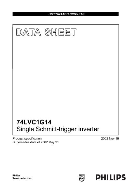
74LVC1G14 Single Schmitt-trigger inverter - Glacier
74LVC1G14 Single Schmitt-trigger inverter - Glacier
74LVC1G14 Single Schmitt-trigger inverter - Glacier

You also want an ePaper? Increase the reach of your titles
YUMPU automatically turns print PDFs into web optimized ePapers that Google loves.
INTEGRATED CIRCUITS<br />
DATA SHEET<br />
<strong>74LVC1G14</strong><br />
<strong>Single</strong> <strong>Schmitt</strong>-<strong>trigger</strong> <strong>inverter</strong><br />
Product specification<br />
Supersedes data of 2002 May 21<br />
2002 Nov 19
Philips Semiconductors<br />
Product specification<br />
<strong>Single</strong> <strong>Schmitt</strong>-<strong>trigger</strong> <strong>inverter</strong><br />
<strong>74LVC1G14</strong><br />
FEATURES<br />
• Wide supply voltage range from 1.65 to 5.5 V<br />
• High noise immunity<br />
• Complies with JEDEC standard:<br />
– JESD8-7 (1.65 to 1.95 V)<br />
– JESD8-5 (2.3 to 2.7 V)<br />
– JESD8B/JESD36 (2.7 to 3.6 V).<br />
• ±24 mA output drive (V CC = 3.0 V)<br />
• CMOS low power consumption<br />
• Latch-up performance exceeds 250 mA<br />
• Direct interface with TTL levels<br />
• Unlimited rise and fall times<br />
• Input accepts voltages up to 5 V<br />
• Multiple package options<br />
• ESD protection:<br />
HBM EIA/JESD22-A114-A exceeds 2000 V<br />
MM EIA/JESD22-A115-A exceeds 200 V.<br />
• Specified from −40 to +125 °C.<br />
DESCRIPTION<br />
The <strong>74LVC1G14</strong> is a high-performance, low-power,<br />
low-voltage, Si-gate CMOS device, superior to most<br />
advanced CMOS compatible TTL families.<br />
The input can be driven from either 3.3 or 5 V devices.<br />
This feature allows the use of this device in a mixed<br />
3.3 and 5 V environment.<br />
<strong>Schmitt</strong>-<strong>trigger</strong> action at the input makes the circuit<br />
tolerant for slower input rise and fall time.<br />
This device is fully specified for partial power-down<br />
applications using I off . The I off circuitry disables the output,<br />
preventing the damaging backflow current through the<br />
device when it is powered down.<br />
The <strong>74LVC1G14</strong> provides the inverting buffer function with<br />
<strong>Schmitt</strong>-<strong>trigger</strong> action.<br />
QUICK REFERENCE DATA<br />
Ground = 0 V; T amb =25°C; t r =t f ≤2.5 ns.<br />
SYMBOL PARAMETER CONDITIONS TYPICAL UNIT<br />
t PHL /t PLH propagation delay A to Y V CC = 1.8 V; C L = 30 pF; R L =1kΩ 4.1 ns<br />
V CC = 2.5 V; C L = 30 pF; R L = 500 Ω 2.8 ns<br />
V CC = 3.3 V; C L = 50 pF; R L = 500 Ω 3.0 ns<br />
V CC = 5.0 V; C L = 50 pF; R L = 500 Ω 2.2 ns<br />
C I input capacitance 5 pF<br />
C PD power dissipation capacitance per buffer notes 1 and 2 15.4 pF<br />
Notes<br />
1. C PD is used to determine the dynamic power dissipation (P D in µW).<br />
P D =C PD × V 2 CC × f i × N+Σ(C L × V 2 CC × f o ) where:<br />
f i = input frequency in MHz;<br />
f o = output frequency in MHz;<br />
C L = output load capacitance in pF;<br />
V CC = supply voltage in Volts;<br />
N = total switching outputs;<br />
Σ(C L × V 2 CC × f o ) = sum of the outputs.<br />
2. The condition is V I = GND to V CC .<br />
2002 Nov 19 2
Philips Semiconductors<br />
Product specification<br />
<strong>Single</strong> <strong>Schmitt</strong>-<strong>trigger</strong> <strong>inverter</strong><br />
<strong>74LVC1G14</strong><br />
FUNCTION TABLE<br />
See note 1.<br />
INPUT<br />
A<br />
L<br />
H<br />
OUTPUT<br />
Y<br />
H<br />
L<br />
Note<br />
1. H = HIGH voltage level;<br />
L = LOW voltage level.<br />
ORDERING INFORMATION<br />
PACKAGE<br />
TYPE NUMBER TEMPERATURE<br />
RANGE<br />
PINS PACKAGE MATERIAL CODE MARKING<br />
<strong>74LVC1G14</strong>GW −40 to +125 °C 5 SC-88A plastic SOT353 VF<br />
<strong>74LVC1G14</strong>GV −40 to +125 °C 5 SC-74A plastic SOT753 V14<br />
PINNING<br />
PIN SYMBOL DESCRIPTION<br />
1 n.c. not connected<br />
2 A data input A<br />
3 GND ground (0 V)<br />
4 Y data output Y<br />
5 V CC supply voltage<br />
handbook, halfpage<br />
n.c<br />
A<br />
1<br />
2<br />
14<br />
5<br />
V CC<br />
handbook, halfpage<br />
A<br />
Y<br />
2 4<br />
GND<br />
3<br />
4<br />
Y<br />
MNA023<br />
MNA022<br />
Fig.1 Pin configuration.<br />
Fig.2 Logic symbol.<br />
2002 Nov 19 3
Philips Semiconductors<br />
Product specification<br />
<strong>Single</strong> <strong>Schmitt</strong>-<strong>trigger</strong> <strong>inverter</strong><br />
<strong>74LVC1G14</strong><br />
handbook, halfpage<br />
2 4<br />
handbook, halfpage<br />
A<br />
Y<br />
MNA024<br />
MNA025<br />
Fig.3 IEE/IEC logic symbol.<br />
Fig.4 Logic diagram.<br />
RECOMMENDED OPERATING CONDITIONS<br />
SYMBOL PARAMETER CONDITIONS MIN. MAX. UNIT<br />
V CC supply voltage 1.65 5.5 V<br />
V I input voltage 0 5.5 V<br />
V O output voltage active mode 0 V CC V<br />
Power-down mode; V CC = 0 V 0 5.5 V<br />
T amb operating ambient temperature −40 +125 °C<br />
t r ,t f input rise and fall times V CC = 1.65 to 2.7 V 0 20 ns/V<br />
V CC = 2.7 to 5.5 V 0 10 ns/V<br />
LIMITING VALUES<br />
In accordance with the Absolute Maximum Rating System (IEC 60134); voltages are referenced to GND (ground = 0 V).<br />
SYMBOL PARAMETER CONDITIONS MIN. MAX. UNIT<br />
V CC supply voltage −0.5 +6.5 V<br />
I IK input diode current V I V CC or V O
Philips Semiconductors<br />
Product specification<br />
<strong>Single</strong> <strong>Schmitt</strong>-<strong>trigger</strong> <strong>inverter</strong><br />
<strong>74LVC1G14</strong><br />
DC CHARACTERISTICS<br />
At recommended operating conditions; voltages are referenced to GND (ground =0V).<br />
SYMBOL<br />
PARAMETER<br />
TEST CONDITIONS<br />
OTHER<br />
T amb = −40 to +85 °C<br />
V OL LOW-level output voltage V I =V CC or GND;<br />
I O = 100 µA<br />
V I =V CC or GND;<br />
I O =4mA<br />
V I =V CC or GND;<br />
I O =8mA<br />
V I =V CC or GND;<br />
I O =12mA<br />
V I =V CC or GND;<br />
I O =24mA<br />
V I =V CC or GND;<br />
I O =32mA<br />
V OH<br />
HIGH-level output<br />
voltage<br />
V I =V CC or GND;<br />
I O = −100 µA<br />
V I =V CC or GND;<br />
I O = −4 mA<br />
V I =V CC or GND;<br />
I O = −8 mA<br />
V I =V CC or GND;<br />
I O = −12 mA<br />
V I =V CC or GND;<br />
I O = −24 mA<br />
V I =V CC or GND;<br />
I O =−32 mA<br />
V CC (V)<br />
MIN. TYP. (1) MAX. UNIT<br />
1.65 to 5.5 − − 0.1 V<br />
1.65 − − 0.45 V<br />
2.3 − − 0.3 V<br />
2.7 − − 0.4 V<br />
3.0 − − 0.55 V<br />
4.5 − − 0.55 V<br />
1.65 to 5.5 V CC − 0.1 − − V<br />
1.65 1.2 − − V<br />
2.3 1.9 − − V<br />
2.7 2.2 − − V<br />
3.0 2.3 − − V<br />
4.5 3.8 − − V<br />
I LI input leakage current V I = 5.5 V or GND 3.6 − ±0.1 ±5 µA<br />
I off power OFF leakage V I or V O = 5.5 V 0 − ±0.1 ±10 µA<br />
current<br />
I CC quiescent supply current V I =V CC or GND;<br />
I O =0<br />
5.5 − 0.1 10 µA<br />
∆I CC<br />
additional quiescent<br />
supply current per pin<br />
V I =V CC − 0.6 V;<br />
I O =0<br />
2.3 to 5.5 − 5 500 µA<br />
2002 Nov 19 5
Philips Semiconductors<br />
Product specification<br />
<strong>Single</strong> <strong>Schmitt</strong>-<strong>trigger</strong> <strong>inverter</strong><br />
<strong>74LVC1G14</strong><br />
SYMBOL<br />
T amb = −40 to +125 °C<br />
V OL LOW-level output voltage V I =V CC or GND;<br />
I O = 100 µA<br />
V I =V CC or GND;<br />
I O =4mA<br />
V I =V CC or GND;<br />
I O =8mA<br />
V I =V CC or GND;<br />
I O =12mA<br />
V I =V CC or GND;<br />
I O =24mA<br />
V I =V CC or GND;<br />
I O =32mA<br />
V OH<br />
HIGH-level output<br />
voltage<br />
V I =V CC or GND;<br />
I O = −100 µA<br />
V I =V CC or GND;<br />
I O = −4 mA<br />
V I =V CC or GND;<br />
I O = −8 mA<br />
V I =V CC or GND;<br />
I O = −12 mA<br />
V I =V CC or GND;<br />
I O = −24 mA<br />
V I =V CC or GND;<br />
I O =−32 mA<br />
Note<br />
1. All typical values are measured at maximum V CC and T amb =25°C.<br />
1.65 to 5.5 − − 0.1 V<br />
1.65 − − 0.7 V<br />
2.3 − − 0.45 V<br />
2.7 − − 0.6 V<br />
3.0 − − 0.8 V<br />
4.5 − − 0.8 V<br />
1.65 to 5.5 V CC − 0.1 − − V<br />
1.65 0.95 − − V<br />
2.3 1.7 − − V<br />
2.7 1.9 − − V<br />
3.0 2.0 − − V<br />
4.5 3.4 − − V<br />
I LI input leakage current V I = 5.5 V or GND 3.6 − − ±100 µA<br />
I off power OFF leakage V I or V O = 5.5 V 0 − − ±200 µA<br />
current<br />
I CC quiescent supply current V I =V CC or GND;<br />
I O =0<br />
5.5 − − 200 µA<br />
I CC<br />
PARAMETER<br />
additional quiescent<br />
supply current per pin<br />
TEST CONDITIONS<br />
OTHER<br />
V I =V CC − 0.6 V;<br />
I O =0<br />
V CC (V)<br />
MIN. TYP. (1) MAX. UNIT<br />
2.3 to 5.5 − − 5000 µA<br />
2002 Nov 19 6
Philips Semiconductors<br />
Product specification<br />
<strong>Single</strong> <strong>Schmitt</strong>-<strong>trigger</strong> <strong>inverter</strong><br />
<strong>74LVC1G14</strong><br />
TRANSFER CHARACTERISTICS<br />
At recommended operating conditions; voltages are referenced to GND (ground =0V).<br />
SYMBOL<br />
PARAMETER<br />
T amb = −40 to +85 °C<br />
V T+ positive-going threshold<br />
voltage<br />
V T−<br />
V H<br />
negative-going threshold<br />
voltage<br />
hysteresis voltage<br />
(V T+ − V T− )<br />
T amb = −40 to +125 °C<br />
V T+ positive-going threshold<br />
voltage<br />
V T−<br />
V H<br />
negative-going threshold<br />
voltage<br />
hysteresis voltage<br />
(V T+ − V T− )<br />
TEST CONDITIONS<br />
OTHER V CC (V)<br />
MIN. TYP. (1) MAX. UNIT<br />
see Figs. 7 and 8 1.8 0.82 1.0 1.14 V<br />
2.3 1.03 1.2 1.40 V<br />
3.0 1.29 1.5 1.71 V<br />
4.5 1.84 2.1 2.36 V<br />
5.5 2.19 2.5 2.79 V<br />
see Figs. 7 and 8 1.8 0.46 0.6 0.75 V<br />
2.3 0.65 0.8 0.96 V<br />
3.0 0.88 1.0 1.24 V<br />
4.5 1.32 1.5 1.84 V<br />
5.5 1.58 1.8 2.24 V<br />
see Figs. 7 and 8 1.8 0.26 0.4 0.51 V<br />
2.3 0.28 0.4 0.57 V<br />
3.0 0.31 0.5 0.64 V<br />
4.5 0.40 0.6 0.77 V<br />
5.5 0.47 0.6 0.88 V<br />
see Figs. 7 and 8 1.8 0.79 − 1.14 V<br />
2.3 1.00 − 1.40 V<br />
3.0 1.26 − 1.71 V<br />
4.5 1.81 − 2.36 V<br />
5.5 2.16 − 2.79 V<br />
see Figs. 7 and 8 1.8 0.46 − 0.78 V<br />
2.3 0.65 − 0.99 V<br />
3.0 0.88 − 1.27 V<br />
4.5 1.32 − 1.87 V<br />
5.5 1.58 − 2.27 V<br />
see Figs. 7 and 8 1.8 0.19 − 0.51 V<br />
2.3 0.22 − 0.57 V<br />
3.0 0.25 − 0.64 V<br />
4.5 0.34 − 0.77 V<br />
5.5 0.41 − 0.88 V<br />
Note<br />
1. All typical values are measured at T amb =25°C.<br />
2002 Nov 19 7
Philips Semiconductors<br />
Product specification<br />
<strong>Single</strong> <strong>Schmitt</strong>-<strong>trigger</strong> <strong>inverter</strong><br />
<strong>74LVC1G14</strong><br />
AC CHARACTERISTICS<br />
GND = 0 V; t r =t f ≤2.0 ns.<br />
SYMBOL<br />
PARAMETER<br />
TEST CONDITIONS<br />
OTHER<br />
V CC (V)<br />
MIN. TYP. MAX. UNIT<br />
T amb = −40 to +85 °C<br />
t PHL /t PLH propagation delay A to Y see Figs 5 and 6 1.65 to 1.95 1.0 4.1 11.0 ns<br />
2.3 to 2.7 0.7 2.8 6.5 ns<br />
2.7 0.7 3.2 6.5 ns<br />
3.0 to 3.6 0.7 3.0 5.5 ns<br />
4.5 to 5.5 0.7 2.2 5.0 ns<br />
T amb = −40 to +125 °C<br />
t PHL /t PLH propagation delay A to Y see Figs 5 and 6 1.65 to 1.95 1.0 − 14.0 ns<br />
2.3 to 2.7 0.7 − 8.5 ns<br />
2.7 0.7 − 8.5 ns<br />
3.0 to 3.6 0.7 − 7.0 ns<br />
4.5 to 5.5 0.7 − 6.5 ns<br />
AC WAVEFORMS<br />
handbook, halfpage<br />
V I<br />
A input<br />
V M<br />
GND<br />
V OH<br />
t PHL<br />
t PLH<br />
Y output<br />
V M<br />
V OL<br />
MNA640<br />
V CC V M<br />
INPUT<br />
V I<br />
t r =t f<br />
1.65 to 1.95 V 0.5 × V CC V CC ≤ 2.0 ns<br />
2.3 to 2.7 V 0.5 × V CC V CC ≤ 2.0 ns<br />
2.7 V 1.5 V 2.7 V ≤ 2.5 ns<br />
3.0 to 3.6 V 1.5 V 2.7 V ≤ 2.5 ns<br />
4.5 to 5.5 V 0.5 × V CC V CC ≤ 2.5 ns<br />
V OL and V OH are typical output voltage drop that occur with the output load.<br />
Fig.5 Input A to output Y propagation delay times.<br />
2002 Nov 19 8
Philips Semiconductors<br />
Product specification<br />
<strong>Single</strong> <strong>Schmitt</strong>-<strong>trigger</strong> <strong>inverter</strong><br />
<strong>74LVC1G14</strong><br />
handbook, full pagewidth<br />
V EXT<br />
V CC<br />
V I V O<br />
MNA616<br />
PULSE<br />
GENERATOR<br />
RT<br />
D.U.T.<br />
C L<br />
R L<br />
R L<br />
V EXT<br />
V CC V I C L R L<br />
t PLH /t PHL t PZH /t PHZ t PZL /t PLZ<br />
1.65 to 1.95 V V CC 30 pF 1 kΩ open GND 2 × V CC<br />
2.3 to 2.7 V V CC 30 pF 500 Ω open GND 2 × V CC<br />
2.7 V 2.7 V 50 pF 500 Ω open GND 6 V<br />
3.0 to 3.6 V 2.7 V 50 pF 500 Ω open GND 6 V<br />
4.5 to 5.5 V V CC 50 pF 500 Ω open GND 2 × V CC<br />
Definitions for test circuit:<br />
R L = Load resistor.<br />
C L = Load capacitance including jig and probe capacitance.<br />
R T = Termination resistance should be equal to the output impedance Z o of the pulse generator.<br />
Fig.6 Load circuitry for switching times.<br />
2002 Nov 19 9
Philips Semiconductors<br />
Product specification<br />
<strong>Single</strong> <strong>Schmitt</strong>-<strong>trigger</strong> <strong>inverter</strong><br />
<strong>74LVC1G14</strong><br />
TRANSFER CHARACTERISTIC WAVEFORMS<br />
handbook, halfpage<br />
V O<br />
V H V I<br />
handbook, halfpage<br />
V O<br />
V I<br />
V T+<br />
V T−<br />
V H<br />
MNA027<br />
MNA026<br />
V T−<br />
V T+<br />
Fig.8 Definitions of V T+ , V T− and V H .<br />
Fig.7 Transfer characteristic.<br />
10<br />
handbook, halfpage<br />
I CC<br />
(mA)<br />
8<br />
MNA641<br />
6<br />
4<br />
2<br />
0<br />
0 1 2<br />
V<br />
3<br />
I (V)<br />
Fig.9<br />
Typical transfer characteristics at<br />
V CC = 3.0 V.<br />
2002 Nov 19 10
Philips Semiconductors<br />
Product specification<br />
<strong>Single</strong> <strong>Schmitt</strong>-<strong>trigger</strong> <strong>inverter</strong><br />
<strong>74LVC1G14</strong><br />
APPLICATION INFORMATION<br />
The slow input rise and fall times cause additional power<br />
dissipation, this can be calculated using the following<br />
formula:<br />
P ad =f i ×(t r × I CC(AV) +t f ×I CC(AV) ) × V CC where:<br />
P ad = additional power dissipation (µW);<br />
f i = input frequency (MHz);<br />
t r = input rise time (ns); 10% to 90%;<br />
t f = input fall time (ns); 90% to 10%;<br />
I CC(AV) = average additional supply current (µA).<br />
Average I CC differs with positive or negative input<br />
transitions, as shown in Fig.10.<br />
An example of a relaxation circuit using the <strong>74LVC1G14</strong> is<br />
shown in Fig.11.<br />
Remark to the application information<br />
All values given are typical values unless otherwise<br />
specified.<br />
12<br />
handbook, halfpage<br />
average<br />
I CC<br />
10<br />
(mA)<br />
8<br />
6<br />
4<br />
2<br />
positive-going<br />
edge<br />
MNA642<br />
negative-going<br />
edge<br />
0<br />
0 2 4 V 6<br />
CC (V)<br />
Fig.10 Average I CC for 74LVC1G <strong>Schmitt</strong>-<strong>trigger</strong><br />
devices; linear change of V I between<br />
0.8 to 2.0 V.<br />
handbook, halfpage<br />
R<br />
C<br />
MNA035<br />
1 1<br />
f = --<br />
T<br />
≈ 0.5 ---------------------- × RC<br />
Fig.11 Example of a relaxation oscillator.<br />
2002 Nov 19 11
Philips Semiconductors<br />
Product specification<br />
<strong>Single</strong> <strong>Schmitt</strong>-<strong>trigger</strong> <strong>inverter</strong><br />
<strong>74LVC1G14</strong><br />
PACKAGE OUTLINES<br />
Plastic surface mounted package; 5 leads<br />
SOT353<br />
D<br />
B<br />
E<br />
A<br />
X<br />
y<br />
H E<br />
v M<br />
A<br />
5<br />
4<br />
Q<br />
A<br />
1 2 3<br />
A1<br />
c<br />
e1<br />
bp<br />
w M<br />
B<br />
Lp<br />
e<br />
detail X<br />
0 1 2 mm<br />
scale<br />
DIMENSIONS (mm are the original dimensions)<br />
UNIT A<br />
A 1<br />
max<br />
mm<br />
1.1<br />
0.8<br />
0.1<br />
bp c D E (2) e e 1 H E L p Q v w y<br />
0.30<br />
0.20<br />
0.25<br />
0.10<br />
2.2<br />
1.8<br />
1.35<br />
1.15<br />
1.3<br />
0.65<br />
2.2<br />
2.0<br />
0.45<br />
0.15<br />
0.25<br />
0.15<br />
0.2<br />
0.2 0.1<br />
OUTLINE<br />
VERSION<br />
REFERENCES<br />
IEC JEDEC EIAJ<br />
EUROPEAN<br />
PROJECTION<br />
ISSUE DATE<br />
SOT353<br />
SC-88A<br />
97-02-28<br />
2002 Nov 19 12
Philips Semiconductors<br />
Product specification<br />
<strong>Single</strong> <strong>Schmitt</strong>-<strong>trigger</strong> <strong>inverter</strong><br />
<strong>74LVC1G14</strong><br />
Plastic surface mounted package; 5 leads<br />
SOT753<br />
D<br />
B<br />
E<br />
A<br />
X<br />
y<br />
H E<br />
v M<br />
A<br />
5<br />
4<br />
Q<br />
A<br />
A1<br />
c<br />
1 2<br />
3<br />
Lp<br />
e<br />
bp<br />
w M<br />
B<br />
detail X<br />
0 1 2 mm<br />
scale<br />
DIMENSIONS (mm are the original dimensions)<br />
UNIT A A 1 bp c D E e H E L p Q v w y<br />
mm<br />
1.1<br />
0.9<br />
0.100<br />
0.013<br />
0.40<br />
0.25<br />
0.26<br />
0.10<br />
3.1<br />
2.7<br />
1.7<br />
1.3<br />
0.95<br />
3.0<br />
2.5<br />
0.6<br />
0.2<br />
0.33<br />
0.23<br />
0.2<br />
0.2 0.1<br />
OUTLINE<br />
VERSION<br />
REFERENCES<br />
IEC JEDEC JEITA<br />
EUROPEAN<br />
PROJECTION<br />
ISSUE DATE<br />
SOT753<br />
SC-74A<br />
02-04-16<br />
2002 Nov 19 13
Philips Semiconductors<br />
Product specification<br />
<strong>Single</strong> <strong>Schmitt</strong>-<strong>trigger</strong> <strong>inverter</strong><br />
<strong>74LVC1G14</strong><br />
SOLDERING<br />
Introduction to soldering surface mount packages<br />
This text gives a very brief insight to a complex technology.<br />
A more in-depth account of soldering ICs can be found in<br />
our “Data Handbook IC26; Integrated Circuit Packages”<br />
(document order number 9398 652 90011).<br />
There is no soldering method that is ideal for all surface<br />
mount IC packages. Wave soldering can still be used for<br />
certain surface mount ICs, but it is not suitable for fine pitch<br />
SMDs. In these situations reflow soldering is<br />
recommended.<br />
Reflow soldering<br />
Reflow soldering requires solder paste (a suspension of<br />
fine solder particles, flux and binding agent) to be applied<br />
to the printed-circuit board by screen printing, stencilling or<br />
pressure-syringe dispensing before package placement.<br />
Several methods exist for reflowing; for example,<br />
convection or convection/infrared heating in a conveyor<br />
type oven. Throughput times (preheating, soldering and<br />
cooling) vary between 100 and 200 seconds depending<br />
on heating method.<br />
Typical reflow peak temperatures range from<br />
215 to 250 °C. The top-surface temperature of the<br />
packages should preferable be kept below 220 °C for<br />
thick/large packages, and below 235 °C for small/thin<br />
packages.<br />
Wave soldering<br />
Conventional single wave soldering is not recommended<br />
for surface mount devices (SMDs) or printed-circuit boards<br />
with a high component density, as solder bridging and<br />
non-wetting can present major problems.<br />
To overcome these problems the double-wave soldering<br />
method was specifically developed.<br />
If wave soldering is used the following conditions must be<br />
observed for optimal results:<br />
• Use a double-wave soldering method comprising a<br />
turbulent wave with high upward pressure followed by a<br />
smooth laminar wave.<br />
• For packages with leads on two sides and a pitch (e):<br />
– larger than or equal to 1.27 mm, the footprint<br />
longitudinal axis is preferred to be parallel to the<br />
transport direction of the printed-circuit board;<br />
– smaller than 1.27 mm, the footprint longitudinal axis<br />
must be parallel to the transport direction of the<br />
printed-circuit board.<br />
The footprint must incorporate solder thieves at the<br />
downstream end.<br />
• For packages with leads on four sides, the footprint must<br />
be placed at a 45° angle to the transport direction of the<br />
printed-circuit board. The footprint must incorporate<br />
solder thieves downstream and at the side corners.<br />
During placement and before soldering, the package must<br />
be fixed with a droplet of adhesive. The adhesive can be<br />
applied by screen printing, pin transfer or syringe<br />
dispensing. The package can be soldered after the<br />
adhesive is cured.<br />
Typical dwell time is 4 seconds at 250 °C.<br />
A mildly-activated flux will eliminate the need for removal<br />
of corrosive residues in most applications.<br />
Manual soldering<br />
Fix the component by first soldering two<br />
diagonally-opposite end leads. Use a low voltage (24 V or<br />
less) soldering iron applied to the flat part of the lead.<br />
Contact time must be limited to 10 seconds at up to<br />
300 °C.<br />
When using a dedicated tool, all other leads can be<br />
soldered in one operation within 2 to 5 seconds between<br />
270 and 320 °C.<br />
2002 Nov 19 14
Philips Semiconductors<br />
Product specification<br />
<strong>Single</strong> <strong>Schmitt</strong>-<strong>trigger</strong> <strong>inverter</strong><br />
<strong>74LVC1G14</strong><br />
Suitability of surface mount IC packages for wave and reflow soldering methods<br />
SOLDERING METHOD<br />
PACKAGE (1)<br />
WAVE REFLOW (2)<br />
BGA, LBGA, LFBGA, SQFP, TFBGA, VFBGA not suitable suitable<br />
HBCC, HBGA, HLQFP, HSQFP, HSOP, HTQFP, HTSSOP, HVQFN, not suitable (3) suitable<br />
HVSON, SMS<br />
PLCC (4) , SO, SOJ suitable suitable<br />
LQFP, QFP, TQFP not recommended (4)(5) suitable<br />
SSOP, TSSOP, VSO not recommended (6) suitable<br />
Notes<br />
1. For more detailed information on the BGA packages refer to the “(LF)BGA Application Note” (AN01026); order a copy<br />
from your Philips Semiconductors sales office.<br />
2. All surface mount (SMD) packages are moisture sensitive. Depending upon the moisture content, the maximum<br />
temperature (with respect to time) and body size of the package, there is a risk that internal or external package<br />
cracks may occur due to vaporization of the moisture in them (the so called popcorn effect). For details, refer to the<br />
Drypack information in the “Data Handbook IC26; Integrated Circuit Packages; Section: Packing Methods”.<br />
3. These packages are not suitable for wave soldering. On versions with the heatsink on the bottom side, the solder<br />
cannot penetrate between the printed-circuit board and the heatsink. On versions with the heatsink on the top side,<br />
the solder might be deposited on the heatsink surface.<br />
4. If wave soldering is considered, then the package must be placed at a 45° angle to the solder wave direction.<br />
The package footprint must incorporate solder thieves downstream and at the side corners.<br />
5. Wave soldering is suitable for LQFP, TQFP and QFP packages with a pitch (e) larger than 0.8 mm; it is definitely not<br />
suitable for packages with a pitch (e) equal to or smaller than 0.65 mm.<br />
6. Wave soldering is suitable for SSOP and TSSOP packages with a pitch (e) equal to or larger than 0.65 mm; it is<br />
definitely not suitable for packages with a pitch (e) equal to or smaller than 0.5 mm.<br />
2002 Nov 19 15
Philips Semiconductors<br />
Product specification<br />
<strong>Single</strong> <strong>Schmitt</strong>-<strong>trigger</strong> <strong>inverter</strong><br />
<strong>74LVC1G14</strong><br />
DATA SHEET STATUS<br />
LEVEL<br />
DATA SHEET<br />
STATUS (1)<br />
PRODUCT<br />
STATUS (2)(3)<br />
DEFINITION<br />
I Objective data Development This data sheet contains data from the objective specification for product<br />
development. Philips Semiconductors reserves the right to change the<br />
specification in any manner without notice.<br />
II Preliminary data Qualification This data sheet contains data from the preliminary specification.<br />
Supplementary data will be published at a later date. Philips<br />
Semiconductors reserves the right to change the specification without<br />
notice, in order to improve the design and supply the best possible<br />
product.<br />
III Product data Production This data sheet contains data from the product specification. Philips<br />
Semiconductors reserves the right to make changes at any time in order<br />
to improve the design, manufacturing and supply. Relevant changes will<br />
be communicated via a Customer Product/Process Change Notification<br />
(CPCN).<br />
Notes<br />
1. Please consult the most recently issued data sheet before initiating or completing a design.<br />
2. The product status of the device(s) described in this data sheet may have changed since this data sheet was<br />
published. The latest information is available on the Internet at URL http://www.semiconductors.philips.com.<br />
3. For data sheets describing multiple type numbers, the highest-level product status determines the data sheet status.<br />
DEFINITIONS<br />
Short-form specification ⎯ The data in a short-form<br />
specification is extracted from a full data sheet with the<br />
same type number and title. For detailed information see<br />
the relevant data sheet or data handbook.<br />
Limiting values definition ⎯ Limiting values given are in<br />
accordance with the Absolute Maximum Rating System<br />
(IEC 60134). Stress above one or more of the limiting<br />
values may cause permanent damage to the device.<br />
These are stress ratings only and operation of the device<br />
at these or at any other conditions above those given in the<br />
Characteristics sections of the specification is not implied.<br />
Exposure to limiting values for extended periods may<br />
affect device reliability.<br />
Application information ⎯ Applications that are<br />
described herein for any of these products are for<br />
illustrative purposes only. Philips Semiconductors make<br />
no representation or warranty that such applications will be<br />
suitable for the specified use without further testing or<br />
modification.<br />
DISCLAIMERS<br />
Life support applications ⎯ These products are not<br />
designed for use in life support appliances, devices, or<br />
systems where malfunction of these products can<br />
reasonably be expected to result in personal injury. Philips<br />
Semiconductors customers using or selling these products<br />
for use in such applications do so at their own risk and<br />
agree to fully indemnify Philips Semiconductors for any<br />
damages resulting from such application.<br />
Right to make changes ⎯ Philips Semiconductors<br />
reserves the right to make changes in the products -<br />
including circuits, standard cells, and/or software -<br />
described or contained herein in order to improve design<br />
and/or performance. When the product is in full production<br />
(status ‘Production’), relevant changes will be<br />
communicated via a Customer Product/Process Change<br />
Notification (CPCN). Philips Semiconductors assumes no<br />
responsibility or liability for the use of any of these<br />
products, conveys no licence or title under any patent,<br />
copyright, or mask work right to these products, and<br />
makes no representations or warranties that these<br />
products are free from patent, copyright, or mask work<br />
right infringement, unless otherwise specified.<br />
2002 Nov 19 16
Philips Semiconductors<br />
Product specification<br />
<strong>Single</strong> <strong>Schmitt</strong>-<strong>trigger</strong> <strong>inverter</strong><br />
<strong>74LVC1G14</strong><br />
NOTES<br />
2002 Nov 19 17
Philips Semiconductors<br />
Product specification<br />
<strong>Single</strong> <strong>Schmitt</strong>-<strong>trigger</strong> <strong>inverter</strong><br />
<strong>74LVC1G14</strong><br />
NOTES<br />
2002 Nov 19 18
Philips Semiconductors<br />
Product specification<br />
<strong>Single</strong> <strong>Schmitt</strong>-<strong>trigger</strong> <strong>inverter</strong><br />
<strong>74LVC1G14</strong><br />
NOTES<br />
2002 Nov 19 19
Philips Semiconductors – a worldwide company<br />
Contact information<br />
For additional information please visit http://www.semiconductors.philips.com. Fax: +31 40 27 24825<br />
For sales offices addresses send e-mail to: sales.addresses@www.semiconductors.philips.com.<br />
© Koninklijke Philips Electronics N.V. 2002 SCA74<br />
All rights are reserved. Reproduction in whole or in part is prohibited without the prior written consent of the copyright owner.<br />
The information presented in this document does not form part of any quotation or contract, is believed to be accurate and reliable and may be changed<br />
without notice. No liability will be accepted by the publisher for any consequence of its use. Publication thereof does not convey nor imply any license<br />
under patent- or other industrial or intellectual property rights.<br />
Printed in The Netherlands 613508/04/pp20 Date of release: 2002 Nov 19 Document order number: 9397 750 10072