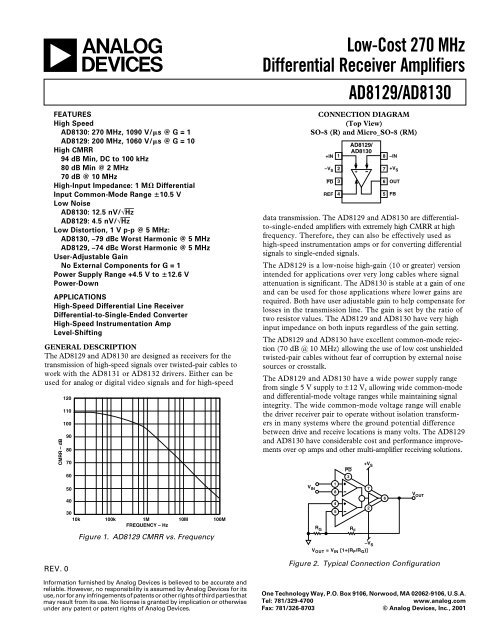
AD8129/AD8130 Low-Cost 270 MHz Differential Receiver ... - KIP
AD8129/AD8130 Low-Cost 270 MHz Differential Receiver ... - KIP
AD8129/AD8130 Low-Cost 270 MHz Differential Receiver ... - KIP

Create successful ePaper yourself
Turn your PDF publications into a flip-book with our unique Google optimized e-Paper software.
a<br />
FEATURES<br />
High Speed<br />
<strong>AD8130</strong>: <strong>270</strong> <strong>MHz</strong>, 1090 V/s @ G = 1<br />
<strong>AD8129</strong>: 200 <strong>MHz</strong>, 1060 V/s @ G = 10<br />
High CMRR<br />
94 dB Min, DC to 100 kHz<br />
80 dB Min @ 2 <strong>MHz</strong><br />
70 dB @ 10 <strong>MHz</strong><br />
High-Input Impedance: 1 M <strong>Differential</strong><br />
Input Common-Mode Range 10.5 V<br />
<strong>Low</strong> Noise<br />
<strong>AD8130</strong>: 12.5 nV/√Hz<br />
<strong>AD8129</strong>: 4.5 nV/√Hz<br />
<strong>Low</strong> Distortion, 1 V p-p @ 5 <strong>MHz</strong>:<br />
<strong>AD8130</strong>, –79 dBc Worst Harmonic @ 5 <strong>MHz</strong><br />
<strong>AD8129</strong>, –74 dBc Worst Harmonic @ 5 <strong>MHz</strong><br />
User-Adjustable Gain<br />
No External Components for G = 1<br />
Power Supply Range +4.5 V to 12.6 V<br />
Power-Down<br />
APPLICATIONS<br />
High-Speed <strong>Differential</strong> Line <strong>Receiver</strong><br />
<strong>Differential</strong>-to-Single-Ended Converter<br />
High-Speed Instrumentation Amp<br />
Level-Shifting<br />
GENERAL DESCRIPTION<br />
The <strong>AD8129</strong> and <strong>AD8130</strong> are designed as receivers for the<br />
transmission of high-speed signals over twisted-pair cables to<br />
work with the AD8131 or AD8132 drivers. Either can be<br />
used for analog or digital video signals and for high-speed<br />
CMRR – dB<br />
120<br />
110<br />
100<br />
90<br />
80<br />
70<br />
60<br />
50<br />
40<br />
<strong>Low</strong>-<strong>Cost</strong> <strong>270</strong> <strong>MHz</strong><br />
<strong>Differential</strong> <strong>Receiver</strong> Amplifiers<br />
<strong>AD8129</strong>/<strong>AD8130</strong><br />
CONNECTION DIAGRAM<br />
(Top View)<br />
SO-8 (R) and Micro_SO-8 (RM)<br />
+IN<br />
1<br />
<strong>AD8129</strong>/<br />
<strong>AD8130</strong><br />
–V S 2<br />
+<br />
7 +V S<br />
PD 3<br />
6 OUT<br />
REF<br />
4<br />
data transmission. The <strong>AD8129</strong> and <strong>AD8130</strong> are differentialto-single-ended<br />
amplifiers with extremely high CMRR at high<br />
frequency. Therefore, they can also be effectively used as<br />
high-speed instrumentation amps or for converting differential<br />
signals to single-ended signals.<br />
The <strong>AD8129</strong> is a low-noise high-gain (10 or greater) version<br />
intended for applications over very long cables where signal<br />
attenuation is significant. The <strong>AD8130</strong> is stable at a gain of one<br />
and can be used for those applications where lower gains are<br />
required. Both have user adjustable gain to help compensate for<br />
losses in the transmission line. The gain is set by the ratio of<br />
two resistor values. The <strong>AD8129</strong> and <strong>AD8130</strong> have very high<br />
input impedance on both inputs regardless of the gain setting.<br />
The <strong>AD8129</strong> and <strong>AD8130</strong> have excellent common-mode rejection<br />
(70 dB @ 10 <strong>MHz</strong>) allowing the use of low cost unshielded<br />
twisted-pair cables without fear of corruption by external noise<br />
sources or crosstalk.<br />
The <strong>AD8129</strong> and <strong>AD8130</strong> have a wide power supply range<br />
from single 5 V supply to ± 12 V, allowing wide common-mode<br />
and differential-mode voltage ranges while maintaining signal<br />
integrity. The wide common-mode voltage range will enable<br />
the driver receiver pair to operate without isolation transformers<br />
in many systems where the ground potential difference<br />
between drive and receive locations is many volts. The <strong>AD8129</strong><br />
and <strong>AD8130</strong> have considerable cost and performance improvements<br />
over op amps and other multi-amplifier receiving solutions.<br />
PD<br />
+V S<br />
8<br />
5<br />
–IN<br />
FB<br />
V OUT<br />
V IN<br />
R G<br />
REV. 0<br />
30<br />
10k 100k 1M 10M 100M<br />
FREQUENCY – Hz<br />
Figure 1. <strong>AD8129</strong> CMRR vs. Frequency<br />
Information furnished by Analog Devices is believed to be accurate and<br />
reliable. However, no responsibility is assumed by Analog Devices for its<br />
use, nor for any infringements of patents or other rights of third parties that<br />
may result from its use. No license is granted by implication or otherwise<br />
under any patent or patent rights of Analog Devices.<br />
R F<br />
–V S<br />
V OUT = V IN [1+(R F /R G )]<br />
Figure 2. Typical Connection Configuration<br />
One Technology Way, P.O. Box 9106, Norwood, MA 02062-9106, U.S.A.<br />
Tel: 781/329-4700<br />
www.analog.com<br />
Fax: 781/326-8703 © Analog Devices, Inc., 2001
<strong>AD8129</strong>/<strong>AD8130</strong>–SPECIFICATIONS<br />
5 V SPECIFICATIONS<br />
(<strong>AD8129</strong> G = 10, <strong>AD8130</strong> G = 1, T A = 25C, V S = 5 V, REF = 0 V, PD ≥ V IH , R L = 1 k, C L = 2 pF, unless<br />
otherwise noted. T MIN to T MAX = –40C to +85C, unless otherwise noted.)<br />
Model <strong>AD8129</strong>A <strong>AD8130</strong>A<br />
Parameter Conditions Min Typ Max Min Typ Max Unit<br />
DYNAMIC PERFORMANCE<br />
–3 dB Bandwidth V OUT ≤ 0.3 V p-p 175 200 240 <strong>270</strong> <strong>MHz</strong><br />
V OUT = 2 V p-p 170 190 140 155 <strong>MHz</strong><br />
Bandwidth for 0.1 dB Flatness V OUT ≤ 0.3 V p-p, SOIC/µSOIC 30/50 45 <strong>MHz</strong><br />
Slew Rate V OUT = 2 V p-p, 25% to 75% 925 1060 950 1090 V/µs<br />
Settling Time V OUT = 2 V p-p, 0.1% 20 20 ns<br />
Rise and Fall Time V OUT ≤ 1 V p-p, 10% to 90% 1.7 1.4 ns<br />
Output Overdrive Recovery 30 40 ns<br />
NOISE/DISTORTION<br />
Second Harmonic/Third Harmonic V OUT = 1 V p-p, 5 <strong>MHz</strong> –74/–84 –79/–86 dBc<br />
V OUT = 2 V p-p, 5 <strong>MHz</strong> –68/–74 –74/–81 dBc<br />
V OUT = 1 V p-p, 10 <strong>MHz</strong> –67/–81 –74/–80 dBc<br />
V OUT = 1 V p-p, 10 <strong>MHz</strong> –61/–70 –74/–76 dBc<br />
IMD V OUT = 2 V p-p, 10 <strong>MHz</strong> –67 –70 dBc<br />
Output IP3 V OUT = 2 V p-p, 10 <strong>MHz</strong> 25 26 dBm<br />
Input Voltage Noise (RTI) f ≥ 10 kHz 4.5 12.5 nV/√Hz<br />
Input Current Noise (+IN, –IN) f ≥ 100 kHz 1 1 pA/√Hz<br />
Input Current Noise (REF, FB) f ≥ 100 kHz 1.4 1.4 pA/√Hz<br />
<strong>Differential</strong> Gain Error <strong>AD8130</strong>, G = 2, NTSC 200 IRE, R L ≥ 150 Ω 0.3 0.13 %<br />
<strong>Differential</strong> Phase Error <strong>AD8130</strong>, G = 2, NTSC 200 IRE, R L ≥ 150 Ω 0.1 0.15 Degrees<br />
INPUT CHARACTERISTICS<br />
Common-Mode Rejection Ratio DC to 100 kHz, V CM = –3 V to +3.5 V 94 110 90 110 dB<br />
V CM = 1 V p-p @ 2 <strong>MHz</strong> 80 80 dB<br />
V CM = 1 V p-p @ 10 <strong>MHz</strong> 70 70 dB<br />
CMRR with V OUT = 1 V p-p V CM = 2 V p-p @ 1 kHz, V OUT = ±0.5 V dc 100 83 dB<br />
Common-Mode Voltage Range V +IN – V –IN = 0 V ±3.5 ±3.8 V<br />
<strong>Differential</strong> Operating Range ±0.5 ±2.5 V<br />
<strong>Differential</strong> Clipping Level ±0.6 ±0.75 ±0.85 ±2.3 ±2.8 ±3.3 V<br />
Resistance <strong>Differential</strong> 1 6 MΩ<br />
Common-Mode 4 4 MΩ<br />
Capacitance <strong>Differential</strong> 3 3 pF<br />
Common-Mode 4 4 pF<br />
DC PERFORMANCE<br />
Closed-Loop Gain Error V OUT = ±1 V, R L ≥ 150 Ω ±0.4 ±1.5 ±0.15 ±0.6 %<br />
T MIN to T MAX 20 10 ppm/°C<br />
Open-Loop Gain V OUT = ±1 V 88 74 dB<br />
Gain Nonlinearity V OUT = ±1 V 250 200 ppm<br />
Input Offset Voltage 0.2 0.8 0.4 1.8 mV<br />
T MIN to T MAX 2 10 µV/°C<br />
T MIN to T MAX 1.4 3.5 mV<br />
Input Offset Voltage vs. Supply +V S = +5 V, –V S = –4.5 V to –5.5 V –90 –84 –78 –74 dB<br />
–V S = –5 V, +V S = +4.5 V to +5.5 V –94 –86 –80 –74 dB<br />
Input Bias Current (+IN, –IN) ±0.5 ±2 ±0.5 ±2 µA<br />
Input Bias Current (REF, FB) ±1 ±3.5 ±1 ±3.5 µA<br />
T MIN to T MAX (+IN, –IN, REF, FB) 5 5 nA/°C<br />
Input Offset Current (+IN, –IN, REF, FB) ±0.08 ±0.4 ±0.08 ±0.4 µA<br />
T MIN to T MAX 0.2 0.2 nA/°C<br />
OUTPUT PERFORMANCE<br />
Voltage Swing R LOAD = 150 Ω/1 kΩ 3.6/4.0 3.6/4.0 ±V<br />
Output Current 40 40 mA<br />
Short Circuit Current To Common –60/+55 –60/+55 mA<br />
T MIN to T MAX –240 –240 µA/°C<br />
Output Impedance PD ≤ V IL , In Power-Down Mode 10 10 pF<br />
POWER SUPPLY<br />
Operating Voltage Range Total Supply Voltage ±2.25 ±12.6 ±2.25 ±12.6 V<br />
Quiescent Supply Current 10.8 11.6 10.8 11.6 mA<br />
T MIN to T MAX 36 36 µA/°C<br />
PD ≤ V IL 0.68 0.85 0.68 0.85 mA<br />
PD ≤ V IL , T MIN to T MAX 1 1 mA<br />
PD PIN<br />
V IH +V S – 1.5 +V S – 1.5 V<br />
V IL +V S – 2.5 +V S – 2.5 V<br />
I IH PD = Min V IH –30 –30 µA<br />
I IL PD = Max V IL –50 –50 µA<br />
Input Resistance PD ≤ +V S – 3 V 12.5 12.5 kΩ<br />
PD ≥ +V S – 2 V 100 100 kΩ<br />
Enable Time 0.5 0.5 µs<br />
Specifications subject to change without notice.<br />
–2–<br />
REV. 0
12 V SPECIFICATIONS<br />
<strong>AD8129</strong>/<strong>AD8130</strong><br />
(<strong>AD8129</strong> G = 10, <strong>AD8130</strong> G = 1, T A = 25C, V S = 12 V, REF = 0 V, PD ≥ V IH , R L = 1 k, C L = 2 pF,<br />
unless otherwise noted. T MIN to T MAX = –40C to +85C, unless otherwise noted.)<br />
Model <strong>AD8129</strong>A <strong>AD8130</strong>A<br />
Parameter Conditions Min Typ Max Min Typ Max Unit<br />
DYNAMIC PERFORMANCE<br />
–3 dB Bandwidth V OUT ≤ 0.3 V p-p 175 200 250 290 <strong>MHz</strong><br />
V OUT = 2 V p-p 170 195 150 175 <strong>MHz</strong><br />
Bandwidth for 0.1 dB Flatness V OUT ≤ 0.3 V p-p, SOIC/µSOIC 50/70 110 <strong>MHz</strong><br />
Slew Rate V OUT = 2 V p-p, 25% to 75% 935 1070 960 1100 V/µs<br />
Settling Time V OUT = 2 V p-p, 0.1% 20 20 ns<br />
Rise and Fall Time V OUT ≤ 1 V p-p, 10% to 90% 1.7 1.4 ns<br />
Output Overdrive Recovery 40 40 ns<br />
NOISE/DISTORTION<br />
Second Harmonic/Third Harmonic V OUT = 1 V p-p, 5 <strong>MHz</strong> –71/–84 –79/–86 dBc<br />
V OUT = 2 V p-p, 5 <strong>MHz</strong> –65/–74 –74/–81 dBc<br />
V OUT = 1 V p-p, 10 <strong>MHz</strong> –65/–82 –74/–80 dBc<br />
V OUT = 2 V p-p, 10 <strong>MHz</strong> –59/–70 –74/–74 dBc<br />
IMD V OUT = 2 V p-p, 10 <strong>MHz</strong> –67 –70 dBc<br />
Output IP3 V OUT = 2 V p-p, 10 <strong>MHz</strong> 25 26 dBm<br />
Input Voltage Noise (RTI) f ≥ 10 kHz 4.6 13 nV/√Hz<br />
Input Current Noise (+IN, –IN) f ≥ 100 kHz 1 1 pA/√Hz<br />
Input Current Noise (REF, FB) f ≥ 100 kHz 1.4 1.4 pA/√Hz<br />
<strong>Differential</strong> Gain Error <strong>AD8130</strong>, G = 2, NTSC 200 IRE, R L ≥ 150 Ω 0.3 0.13 %<br />
<strong>Differential</strong> Phase Error <strong>AD8130</strong>, G = 2, NTSC 200 IRE, R L ≥ 150 Ω 0.1 0.2 Degrees<br />
INPUT CHARACTERISTICS<br />
Common-Mode Rejection Ratio DC to 100 kHz, V CM = ±10 V 92 105 88 105 dB<br />
V CM = 1 V p-p @ 2 <strong>MHz</strong> 80 80 dB<br />
V CM = 1 V p-p @ 10 <strong>MHz</strong> 70 70 dB<br />
CMRR with V OUT = 1 V p-p V CM = 4 V p-p @ 1 kHz, V OUT = ±0.5 V dc 93 80 dB<br />
Common-Mode Voltage Range V +IN – V –IN = 0 V ± 10.3 ± 10.5 V<br />
<strong>Differential</strong> Operating Range ± 0.5 ± 2.5 V<br />
<strong>Differential</strong> Clipping Level ± 0.6 ± 0.75 ± 0.85 ± 2.3 ± 2.8 ± 3.3 V<br />
Resistance <strong>Differential</strong> 1 6 MΩ<br />
Common-Mode 4 4 MΩ<br />
Capacitance <strong>Differential</strong> 3 3 pF<br />
Common-Mode 4 4 pF<br />
DC PERFORMANCE<br />
Closed-Loop Gain Error V OUT = ± 1 V, R L ≥ 150 Ω ±0.8 ± 1.8 ± 0.15 ± 0.6 %<br />
T MIN to T MAX 20 10 ppm/°C<br />
Open-Loop Gain V OUT = ± 1 V 87 73 dB<br />
Gain Nonlinearity V OUT = ± 1 V 250 200 ppm<br />
Input Offset Voltage 0.2 0.8 0.4 1.8 mV<br />
T MIN to T MAX 2 10 µV/°C<br />
T MIN to T MAX 1.4 3.5 mV<br />
Input Offset Voltage vs. Supply +V S = +12 V, –V S = –11.0 V to –13.0 V –88 –82 –77 –70 dB<br />
–V S = –12 V, +V S = +11.0 V to +13.0 V –92 –84 –88 –70 dB<br />
Input Bias Current (+IN, –IN) ± 0.25 ± 2 ± 0.25 ± 2 µA<br />
Input Bias Current (REF, FB) ± 0.5 ± 3.5 ± 0.5 ± 3.5 µA<br />
T MIN to T MAX (+IN, –IN, REF, FB) 2.5 2.5 nA/°C<br />
Input Offset Current (+IN, –IN, REF, FB) ± 0.08 ± 0.4 ± 0.08 ± 0.4 µA<br />
T MIN to T MAX 0.2 0.2 nA/°C<br />
OUTPUT PERFORMANCE<br />
Voltage Swing R LOAD = 700 Ω ±10.8 ±10.8 V<br />
Output Current 40 40 mA<br />
Short Circuit Current To Common –60/+55 –60/+55 mA<br />
T MIN to T MAX –240 –240 µA/°C<br />
Output Impedance PD ≤ V IL , In Power-Down Mode 10 10 pF<br />
POWER SUPPLY<br />
Operating Voltage Range Total Supply Voltage ±2.25 ±12.6 ±2.25 ±12.6 V<br />
Quiescent Supply Current 13 13.9 13 13.9 mA<br />
T MIN to T MAX 43 43 µA/°C<br />
PD ≤ V IL 0.73 0.9 0.73 0.9 mA<br />
PD ≤ V IL , T MIN to T MAX 1.1 1.1 mA<br />
PD PIN<br />
V IH +V S – 1.5 +V S – 1.5 V<br />
V IL +V S – 2.5 +V S – 2.5 V<br />
I IH PD = Min V IH –30 –30 µA<br />
I IL PD = Max V IL –50 –50 µA<br />
Input Resistance PD ≤ +V S – 3 V 3 3 kΩ<br />
PD ≥ +V S – 2 V 100 100 kΩ<br />
Enable Time 0.5 0.5 µs<br />
Specifications subject to change without notice.<br />
REV. 0 –3–
<strong>AD8129</strong>/<strong>AD8130</strong>–SPECIFICATIONS<br />
5 V SPECIFICATIONS<br />
(<strong>AD8129</strong> G = 10, <strong>AD8130</strong> G = 1, T A = 25C, +V S = 5 V, –V S = 0 V, REF = 2.5 V, PD ≥ V IH , R L = 1 k, C L = 2 pF<br />
unless otherwise noted. T MIN to T MAX = –40C to +85C, unless otherwise noted.)<br />
Model <strong>AD8129</strong>A <strong>AD8130</strong>A<br />
Parameter Conditions Min Typ Max Min Typ Max Unit<br />
DYNAMIC PERFORMANCE<br />
–3 dB Bandwidth V OUT ≤ 0.3 V p-p 160 185 220 250 <strong>MHz</strong><br />
V OUT = 1 V p-p 160 185 180 205 <strong>MHz</strong><br />
Bandwidth for 0.1 dB Flatness V OUT ≤ 0.3 V p-p, SOIC/µSOIC 25/40 25 <strong>MHz</strong><br />
Slew Rate V OUT = 2 V p-p, 25% to 75% 810 930 810 930 V/µs<br />
Settling Time V OUT = 2 V p-p, 0.1% 20 20 ns<br />
Rise and Fall Time V OUT ≤ 1 V p-p, 10% to 90% 1.8 1.5 ns<br />
Output Overdrive Recovery 20 30 ns<br />
NOISE/DISTORTION<br />
Second Harmonic/Third Harmonic V OUT = 1 V p-p, 5 <strong>MHz</strong> –68/–75 –72/–79 dBc<br />
V OUT = 2 V p-p, 5 <strong>MHz</strong> –62/–64 –65/–71 dBc<br />
V OUT = 1 V p-p, 10 <strong>MHz</strong> –63/–70 –60/–62 dBc<br />
V OUT = 2 V p-p, 10 <strong>MHz</strong> –56/–58 –68/–68 dBc<br />
IMD V OUT = 2 V p-p, 10 <strong>MHz</strong> –67 –70 dBc<br />
Output IP3 V OUT = 2 V p-p, 10 <strong>MHz</strong> 25 26 dBm<br />
Input Voltage Noise (RTI) f ≥ 10 kHz 4.5 12.3 nV/√Hz<br />
Input Current Noise (+IN, –IN) f ≥ 100 kHz 1 1 pA/√Hz<br />
Input Current Noise (REF, FB) f ≥ 100 kHz 1.4 1.4 pA/√Hz<br />
<strong>Differential</strong> Gain Error <strong>AD8130</strong>, G = 2, NTSC 100 IRE, R L ≥ 150 Ω 0.3 0.13 %<br />
<strong>Differential</strong> Phase Error <strong>AD8130</strong>, G = 2, NTSC 100 IRE, R L ≥ 150 Ω 0.1 0.15 Degrees<br />
INPUT CHARACTERISTICS<br />
Common-Mode Rejection Ratio DC to 100 kHz, V CM = 1.5 V to 3.5 V 86 96 86 96 dB<br />
V CM = 1 V p-p @ 1 <strong>MHz</strong> 80 80 dB<br />
V CM = 1 V p-p @ 10 <strong>MHz</strong> 70 70 dB<br />
CMRR with V OUT = 1 V p-p V CM = 1 V p-p @ 1 kHz, V OUT = ±0.5 V dc 80 72 dB<br />
Common-Mode Voltage Range V +IN – V –IN = 0 V 1.25 to 3.7 1.25 to 3.8 V<br />
<strong>Differential</strong> Operating Range ± 0.5 ± 2.5 V<br />
<strong>Differential</strong> Clipping Level ± 0.6 ± 0.75 ± 0.85 ± 2.3 ± 2.8 ± 3.3 V<br />
Resistance <strong>Differential</strong> 1 6 MΩ<br />
Common-Mode 4 4 MΩ<br />
Capacitance <strong>Differential</strong> 3 3 pF<br />
Common-Mode 4 4 pF<br />
DC PERFORMANCE<br />
Closed-Loop Gain Error V OUT = ± 1 V, R L ≥ 150 Ω ±0.25 ± 1.25 ± 0.1 ± 0.6 %<br />
T MIN to T MAX 20 20 ppm/°C<br />
Open-Loop Gain V OUT = ± 1 V 86 71 dB<br />
Gain Nonlinearity V OUT = ± 1 V 250 200 ppm<br />
Input Offset Voltage 0.2 0.8 0.4 1.8 mV<br />
T MIN to T MAX 2 10 µV/°C<br />
T MIN to T MAX 1.4 3.5 mV<br />
Input Offset Voltage vs. Supply +V S = 5 V, –V S = –0.5 V to +0.5 V –88 –80 –74 –70 dB<br />
–V S = 0 V, +V S = +4.5 V to +5.5 V –100 –86 –90 –76 dB<br />
Input Bias Current (+IN, –IN) ± 0.5 ± 2 ± 0.5 ± 2 µA<br />
Input Bias Current (REF, FB) ± 1 ± 3.5 ± 1 ± 3.5 µA<br />
T MIN to T MAX (+IN, –IN, REF, FB) 5 5 nA/°C<br />
Input Offset Current (+IN, –IN, REF, FB) ± 0.08 ± 0.4 ± 0.08 ± 0.4 µA<br />
T MIN to T MAX 0.2 0.2 nA/°C<br />
OUTPUT PERFORMANCE<br />
Voltage Swing R LOAD ≥ 150 Ω 1.1 3.9 1.1 3.9 V<br />
Output Current 35 35 mA<br />
Short Circuit Current To Common –60/+55 –60/+55 mA<br />
T MIN to T MAX –240 –240 µA/°C<br />
Output Impedance PD ≤ V IL , In Power-Down Mode 10 10 pF<br />
POWER SUPPLY<br />
Operating Voltage Range Total Supply Voltage ±2.25 ±12.6 ±2.25 ±12.6 V<br />
Quiescent Supply Current 9.9 10.6 9.9 10.6 mA<br />
T MIN to T MAX 33 33 µA/°C<br />
PD ≤ V IL 0.65 0.85 0.65 0.85 mA<br />
PD ≤ V IL , T MIN to T MAX 1 1 mA<br />
PD PIN<br />
V IH +V S – 1.5 +V S – 1.5 V<br />
V IL +V S – 2.5 +V S – 2.5 V<br />
I IH PD = Min V IH –30 –30 µA<br />
I IL PD = Max V IL –50 –50 µA<br />
Input Resistance PD ≤ +V S – 3 V 12.5 12.5 kΩ<br />
PD ≥ +V S – 2 V 100 100 kΩ<br />
Enable Time 0.5 0.5 µs<br />
Specifications subject to change without notice.<br />
–4–<br />
REV. 0
<strong>AD8129</strong>/<strong>AD8130</strong><br />
ABSOLUTE MAXIMUM RATINGS 1, 2<br />
Supply Voltage . . . . . . . . . . . . . . . . . . . . . . . . . . . . . . . . 26.4 V<br />
Power Dissipation . . . . . . . . . . . . . . . . . . . . . Refer to Figure 3<br />
Input Voltage (Any Input) . . . . . . . –V S – 0.3 V to +V S + 0.3 V<br />
<strong>Differential</strong> Input Voltage (<strong>AD8129</strong>) 3 V S ≥ ± 11.5 V . . . ± 0.5 V<br />
<strong>Differential</strong> Input Voltage (<strong>AD8129</strong>) 3 V S < ±11.5 V . . . ± 6.2 V<br />
<strong>Differential</strong> Input Voltage (<strong>AD8130</strong>) . . . . . . . . . . . . . . ± 8.4 V<br />
Storage Temperature . . . . . . . . . . . . . . . . . . –65°C to +150°C<br />
Lead Temperature (Soldering 10 sec) . . . . . . . . . . . . . . 300°C<br />
NOTES<br />
1 Stresses above those listed under Absolute Maximum Ratings may cause permanent<br />
damage to the device. This is a stress rating only; functional operation of the<br />
device at these or any other condition s above those indicated in the operational<br />
section of this specification is not implied. Exposure to absolute maximum rating<br />
conditions for extended periods may affect device reliability.<br />
2 Thermal Resistance measured on SEMI standard 4-layer board.<br />
8-Lead SOIC: θ JA = 121°C/W; 8-Lead Micro_SO: θ JA = 142°C/W<br />
3 Refer to Applications section, Extreme Operating Condition, and Power Dissipation.<br />
MAXIMUM POWER DISSIPATION – Watts<br />
2.0<br />
1.5<br />
1.0<br />
0.5<br />
0<br />
–50<br />
8-LEAD<br />
MICRO_SO<br />
8-LEAD SOIC<br />
PACKAGE<br />
T J (MAX) = 150C<br />
–40 –30 –20 –10 0 10 20 30 40 50 60 70 80 90<br />
AMBIENT TEMPERATURE – C<br />
Figure 3. Maximum Power Dissipation vs. Temperature<br />
CONNECTION DIAGRAM<br />
(Top View)<br />
SO-8 (R) and Micro_SO-8 (RM)<br />
+IN<br />
1<br />
<strong>AD8129</strong>/<br />
<strong>AD8130</strong><br />
8<br />
–IN<br />
–V S 2<br />
+<br />
7 +V S<br />
PD 3<br />
6 OUT<br />
REF<br />
4<br />
5<br />
FB<br />
ORDERING GUIDE<br />
Temperature Package Package Branding<br />
Model Range Description Option Information<br />
<strong>AD8129</strong>AR –40ºC to +85ºC 8-Lead SOIC SO-8<br />
<strong>AD8129</strong>AR-REEL 1 –40ºC to +85ºC 8-Lead SOIC 13" Tape and Reel<br />
<strong>AD8129</strong>AR-REEL7 2 –40ºC to +85ºC 8-Lead SOIC 7" Tape and Reel<br />
<strong>AD8129</strong>ARM –40ºC to +85ºC 8-Lead Micro_SO RM-8 HQA<br />
<strong>AD8129</strong>ARM-REEL 3 –40ºC to +85ºC 8-Lead Micro_SO 13" Tape and Reel HQA<br />
<strong>AD8129</strong>ARM-REEL7 2 –40ºC to +85ºC 8-Lead Micro_SO 7" Tape and Reel HQA<br />
<strong>AD8129</strong>-EVAL<br />
Evaluation Board with SOIC<br />
<strong>AD8130</strong>AR –40ºC to +85ºC 8-Lead SOIC SO-8<br />
<strong>AD8130</strong>AR-REEL 1 –40ºC to +85ºC 8-Lead SOIC 13" Tape and Reel<br />
<strong>AD8130</strong>AR-REEL7 2 –40ºC to +85ºC 8-Lead SOIC 7" Tape and Reel<br />
<strong>AD8130</strong>ARM –40ºC to +85ºC 8-Lead Micro_SO RM-8 HPA<br />
<strong>AD8130</strong>ARM-REEL 3 –40ºC to +85ºC 8-Lead Micro_SO 13" Tape and Reel HPA<br />
<strong>AD8130</strong>ARM-REEL7 2 –40ºC to +85ºC 8-Lead Micro_SO 7" Tape and Reel HPA<br />
<strong>AD8130</strong>-EVAL<br />
Evaluation Board with SOIC<br />
NOTES<br />
1 13" Reel of 2500 each.<br />
2 7" Reel of 1000 each.<br />
3 13" Reel of 3000 each.<br />
CAUTION<br />
ESD (electrostatic discharge) sensitive device. Electrostatic charges as high as 4000 V readily<br />
accumulate on the human body and test equipment and can discharge without detection. Although<br />
the <strong>AD8129</strong>/<strong>AD8130</strong> features proprietary ESD protection circuitry, permanent damage may occur<br />
on devices subjected to high-energy electrostatic discharges. Therefore, proper ESD precautions<br />
are recommended to avoid performance degradation or loss of functionality.<br />
WARNING!<br />
ESD SENSITIVE DEVICE<br />
REV. 0<br />
–5–
<strong>AD8129</strong>/<strong>AD8130</strong><br />
<strong>AD8130</strong> Frequency Response Characteristics<br />
(G = 1, R L = 1 k, C L = 2 pF, V OUT = 0.3 V p-p, T A = 25C, unless otherwise noted.)<br />
3<br />
2<br />
1<br />
V OUT = 0.3V p-p<br />
V S = 2.5V<br />
3<br />
2<br />
1<br />
V OUT = 1V p-p<br />
V S = 2.5V<br />
3<br />
2<br />
1<br />
V OUT = 2V p-p<br />
V S = 2.5V<br />
GAIN – dB<br />
0<br />
–1<br />
–2<br />
–3<br />
V S = 5V<br />
V S = 12V<br />
GAIN – dB<br />
0<br />
–1<br />
–2<br />
–3<br />
V S = 5V<br />
V S = 12V<br />
GAIN – dB<br />
0<br />
–1<br />
–2<br />
–3<br />
V S = 5V<br />
V S = 12V<br />
–4<br />
–5<br />
–6<br />
–7<br />
1<br />
10 100 400<br />
FREQUENCY – <strong>MHz</strong><br />
TPC 1. <strong>AD8130</strong> Frequency Response<br />
vs. Supply, V OUT = 0.3 V p-p<br />
–4<br />
–5<br />
–6<br />
–7<br />
1<br />
10 100 300<br />
FREQUENCY – <strong>MHz</strong><br />
TPC 2. <strong>AD8130</strong> Frequency Response<br />
vs. Supply, V OUT = 1 V p-p<br />
–4<br />
–5<br />
–6<br />
–7<br />
1<br />
10 100 300<br />
FREQUENCY – <strong>MHz</strong><br />
TPC 3. <strong>AD8130</strong> Frequency Response<br />
vs. Supply, V OUT = 2 V p-p<br />
6<br />
5<br />
V S = 5V<br />
C L = 20pF<br />
0.7<br />
0.6<br />
R L = 1k<br />
V S = 2.5V<br />
0.5<br />
0.4<br />
R L = 150<br />
V S = 2.5V<br />
GAIN – dB<br />
4<br />
3<br />
2<br />
1<br />
0<br />
–1<br />
–2<br />
–3<br />
C L = 10pF<br />
C L = 5pF<br />
C L = 2pF<br />
GAIN – dB<br />
0.5<br />
0.4<br />
0.3<br />
0.2<br />
0.1<br />
0.0<br />
–0.1<br />
–0.2<br />
V S = 5V<br />
V S = 12V<br />
GAIN – dB<br />
0.3<br />
0.2<br />
0.1<br />
0.0<br />
–0.1<br />
–0.2<br />
–0.3<br />
–0.4<br />
V S = 5V<br />
V S = 12V<br />
–4<br />
1<br />
10 100 300<br />
FREQUENCY – <strong>MHz</strong><br />
–0.3<br />
1<br />
10 100 300<br />
FREQUENCY – <strong>MHz</strong><br />
–0.5<br />
1<br />
10 100 300<br />
FREQUENCY – <strong>MHz</strong><br />
TPC 4. <strong>AD8130</strong> Frequency Response<br />
vs. Load Capacitance<br />
TPC 5. <strong>AD8130</strong> Fine Scale Response<br />
vs. Supply, R L = 1 kΩ<br />
TPC 6. <strong>AD8130</strong> Fine Scale Response<br />
vs. Supply, R L = 150 Ω<br />
GAIN – dB<br />
3<br />
2<br />
1<br />
0<br />
–1<br />
–2<br />
–3<br />
–4<br />
–5<br />
–6<br />
–7<br />
1<br />
R L = 150<br />
V S = 2.5V<br />
V S = 5V<br />
V S = 12V<br />
10 100 400<br />
FREQUENCY – <strong>MHz</strong><br />
TPC 7. <strong>AD8130</strong> Frequency Response<br />
vs. Supply, R L = 150 Ω<br />
GAIN – dB<br />
3<br />
2<br />
1<br />
0<br />
–1<br />
–2<br />
–3<br />
–4<br />
–5<br />
–6<br />
–7<br />
1<br />
G = 2<br />
V OUT = 0.3V p-p<br />
V S = 5V<br />
V S = 12V<br />
V S = 2.5V<br />
10 100 300<br />
FREQUENCY – <strong>MHz</strong><br />
TPC 8. <strong>AD8130</strong> Frequency Response<br />
vs. Supply, G = 2, V OUT = 0.3 V p-p<br />
GAIN – dB<br />
3<br />
2<br />
1<br />
0<br />
–1<br />
–2<br />
–3<br />
–4<br />
–5<br />
–6<br />
–7<br />
1<br />
G = 2<br />
V OUT = 2V p-p<br />
V S = 5V<br />
V S = 12V<br />
V S = 2.5V<br />
10 100 300<br />
FREQUENCY – <strong>MHz</strong><br />
TPC 9. <strong>AD8130</strong> Frequency Response<br />
vs. Supply, G = 2, V OUT = 2 V p-p<br />
–6–<br />
REV. 0
<strong>AD8129</strong>/<strong>AD8130</strong><br />
3<br />
2<br />
1<br />
R F = R G = 750<br />
R F = R G = 1k<br />
0.3<br />
0.2<br />
0.1<br />
G = 2<br />
R L = 1k<br />
V S = 2.5V<br />
0.3<br />
0.2<br />
0.1<br />
G = 2<br />
R L = 150<br />
V S = 2.5V<br />
0<br />
0<br />
0<br />
GAIN – dB<br />
–1<br />
–2<br />
–3<br />
–4<br />
–5<br />
R F = R G = 499<br />
R F = R G = 250<br />
G = 2<br />
V S = 5V<br />
GAIN – dB<br />
–0.1<br />
–0.2<br />
–0.3<br />
–0.4<br />
–0.5<br />
V S = 5V<br />
V S = 12V<br />
GAIN – dB<br />
–0.1<br />
–0.2<br />
–0.3<br />
–0.4<br />
–0.5<br />
V S = 5V<br />
V S = 12V<br />
–6<br />
–0.6<br />
–0.6<br />
–7<br />
1<br />
10 100 300<br />
FREQUENCY – <strong>MHz</strong><br />
–0.7<br />
1 10 100<br />
FREQUENCY – <strong>MHz</strong><br />
–0.7<br />
1 10 100<br />
FREQUENCY – <strong>MHz</strong><br />
TPC 10. <strong>AD8130</strong> Frequency<br />
Response for Various R F /R G<br />
TPC 11. <strong>AD8130</strong> Fine Scale Response<br />
vs. Supply, G = 2, R L = 1 kΩ<br />
TPC 12. <strong>AD8130</strong> Fine Scale Response<br />
vs. Supply, G = 2, R L = 150 Ω<br />
GAIN – dB<br />
3<br />
2<br />
1<br />
0<br />
–1<br />
–2<br />
–3<br />
–4<br />
–5<br />
–6<br />
G = 2<br />
R L = 150<br />
V S = 5V<br />
V S = 12V<br />
V S = 2.5V<br />
–7<br />
1 10 100 300<br />
FREQUENCY – <strong>MHz</strong><br />
TPC 13. <strong>AD8130</strong> Frequency Response<br />
vs. Supply, G = 2, R L = 150 Ω<br />
GAIN – dB<br />
0.3<br />
0.2<br />
0.1<br />
0<br />
–0.1<br />
–0.2<br />
–0.3<br />
–0.4<br />
–0.5<br />
–0.6<br />
–0.7<br />
0.1<br />
V OUT = 2V p-p<br />
V S = 2.5V<br />
V S = 2.5V<br />
V S = 5V, 12V<br />
G = 10<br />
V S = 12V<br />
V S = 5V<br />
G = 5<br />
1 10 30<br />
FREQUENCY – <strong>MHz</strong><br />
TPC 14. <strong>AD8130</strong> Fine Scale Response<br />
vs. Supply, G = 5, G = 10, V OUT = 2 V p-p<br />
GAIN – dB<br />
3<br />
2<br />
1<br />
0<br />
–1<br />
–2<br />
–3<br />
–4<br />
–5<br />
–6<br />
–7<br />
0.1<br />
V OUT = 2V p-p<br />
V S = 12V<br />
V S = 5V, 12V<br />
V S = 2.5V<br />
G = 10<br />
G = 5<br />
1 10 100<br />
FREQUENCY – <strong>MHz</strong><br />
TPC 15. <strong>AD8130</strong> Frequency Response<br />
vs. Supply, G = 5, G = 10, V OUT = 2 V p-p<br />
GAIN – dB<br />
3<br />
2<br />
1<br />
0<br />
–1<br />
–2<br />
–3<br />
–4<br />
–5<br />
–6<br />
–7<br />
0.1<br />
R L = 150<br />
G = 10<br />
V S = 2.5V<br />
V S = 5V, 12V<br />
V S = 5V, 12V<br />
G = 5<br />
1 10 100<br />
FREQUENCY – <strong>MHz</strong><br />
TPC 16. <strong>AD8130</strong> Frequency Response<br />
vs. Supply, G = 5, G = 10, R L = 150 Ω<br />
OUTPUT VOLTAGE – dBV<br />
12<br />
6<br />
0<br />
–6<br />
–12<br />
–18<br />
–24<br />
–30<br />
–36<br />
0dB = 1V RMS<br />
–42<br />
V S = 5V<br />
–48<br />
10<br />
100 400<br />
FREQUENCY – <strong>MHz</strong><br />
TPC 17. <strong>AD8130</strong> Frequency Response<br />
for Various Output Levels<br />
50<br />
R G<br />
1<br />
8<br />
4<br />
5<br />
G<br />
1<br />
2<br />
5<br />
10<br />
R F<br />
R F<br />
0<br />
499<br />
8.06k<br />
4.99k<br />
R G<br />
–<br />
499<br />
2k<br />
549<br />
6<br />
TEK P6245<br />
FET PROBE<br />
R L<br />
TPC 18. <strong>AD8130</strong> Basic Frequency<br />
Response Test Circuit<br />
C L<br />
REV. 0<br />
–7–
<strong>AD8129</strong>/<strong>AD8130</strong><br />
<strong>AD8129</strong> Frequency Response Characteristics<br />
(G = 10, R L = 1 k, C L = 2 pF, V OUT = 0.3 V p-p, T A = 25C, unless otherwise noted.)<br />
3<br />
2<br />
1<br />
V OUT = 0.3V p-p<br />
V S = 2.5V<br />
V S = 5V<br />
3<br />
2<br />
1<br />
V OUT = 1V p-p<br />
V S = 2.5V<br />
V S = 5V<br />
3<br />
2<br />
1<br />
V OUT = 2V p-p<br />
V S = 2.5V<br />
GAIN – dB<br />
0<br />
–1<br />
–2<br />
–3<br />
V S = 12V<br />
GAIN – dB<br />
0<br />
–1<br />
–2<br />
–3<br />
V S = 12V<br />
GAIN – dB<br />
0<br />
–1<br />
–2<br />
–3<br />
V S = 5V<br />
V S = 12V<br />
–4<br />
–4<br />
–4<br />
–5<br />
–6<br />
–7<br />
1 10 100 300<br />
FREQUENCY – <strong>MHz</strong><br />
TPC 19. <strong>AD8129</strong> Frequency Response<br />
vs. Supply, V OUT = 0.3 V p-p<br />
–5<br />
–6<br />
–7<br />
1 10 100 300<br />
FREQUENCY – <strong>MHz</strong><br />
TPC 20. <strong>AD8129</strong> Frequency Response<br />
vs. Supply, V OUT = 1 V p-p<br />
–5<br />
–6<br />
–7<br />
1 10 100 300<br />
FREQUENCY – <strong>MHz</strong><br />
TPC 21. <strong>AD8129</strong> Frequency Response<br />
vs. Supply, V OUT = 2 V p-p<br />
4<br />
3<br />
2<br />
1<br />
V S = 5V<br />
C L = 20pF<br />
C L = 10pF<br />
C L = 5pF<br />
C L = 2pF<br />
0.5<br />
0.4<br />
0.3<br />
0.2<br />
R L = 1k<br />
V S = 2.5V<br />
V S = 5V<br />
0.3<br />
0.2<br />
0.1<br />
0<br />
R L = 150<br />
V S = 2.5V<br />
GAIN – dB<br />
0<br />
–1<br />
–2<br />
GAIN – dB<br />
0.1<br />
0<br />
–0.1<br />
V S = 12V<br />
GAIN – dB<br />
–0.1<br />
–0.2<br />
–0.3<br />
V S = 5V<br />
V S = 12V<br />
–3<br />
–4<br />
–5<br />
–6<br />
1 10 100 300<br />
FREQUENCY – <strong>MHz</strong><br />
TPC 22. <strong>AD8129</strong> Frequency Response<br />
vs. Load Capacitance<br />
–0.2<br />
–0.3<br />
–0.4<br />
–0.5<br />
1 10 100 300<br />
FREQUENCY – <strong>MHz</strong><br />
TPC 23. <strong>AD8129</strong> Fine Scale Response<br />
vs. Supply, R L = 1 kΩ<br />
–0.4<br />
–0.5<br />
–0.6<br />
–0.7<br />
1 10 100 300<br />
FREQUENCY – <strong>MHz</strong><br />
TPC 24. <strong>AD8129</strong> Fine Scale Response<br />
vs. Supply, R L = 150 Ω<br />
GAIN – dB<br />
3<br />
2<br />
1<br />
0<br />
–1<br />
–2<br />
–3<br />
–4<br />
–5<br />
–6<br />
–7<br />
10<br />
R L = 150<br />
V S = 2.5V<br />
V S = 5V<br />
V S = 12V<br />
100 300<br />
FREQUENCY – <strong>MHz</strong><br />
TPC 25. <strong>AD8129</strong> Frequency Response<br />
vs. Supply, R L = 150 Ω<br />
GAIN – dB<br />
3<br />
2<br />
1<br />
0<br />
–1<br />
–2<br />
–3<br />
–4<br />
–5<br />
–6<br />
G = 20<br />
V OUT = 0.3V p-p<br />
V S = 2.5V<br />
V S = 5V, 12V<br />
–7<br />
1 10 100 300<br />
FREQUENCY – <strong>MHz</strong><br />
TPC 26. <strong>AD8129</strong> Frequency Response<br />
vs. Supply, G = 20, V OUT = 0.3 V p-p<br />
GAIN – dB<br />
3<br />
2<br />
1<br />
0<br />
–1<br />
–2<br />
–3<br />
–4<br />
–5<br />
–6<br />
G = 20<br />
V OUT = 2V p-p<br />
V S = 2.5V<br />
V S = 5V, 12V<br />
–7<br />
1 10 100 300<br />
FREQUENCY – <strong>MHz</strong><br />
TPC 27. <strong>AD8129</strong> Frequency Response<br />
vs. Supply, G = 20, V OUT = 2 V p-p<br />
–8–<br />
REV. 0
<strong>AD8129</strong>/<strong>AD8130</strong><br />
GAIN – dB<br />
0.8<br />
0.6<br />
0.4<br />
0.2<br />
0<br />
–0.2<br />
0.2<br />
0<br />
–0.2<br />
–0.4<br />
G = 10<br />
V S = 5V<br />
SOIC<br />
SOIC<br />
2k/221<br />
909/100<br />
499/54.9<br />
499/54.9<br />
909/100<br />
2k/221<br />
–0.6<br />
1 10 100 300<br />
FREQUENCY – <strong>MHz</strong><br />
TPC 28. <strong>AD8129</strong> Fine Scale Response<br />
vs. SOIC and µSOIC for Various R F /R G<br />
GAIN – dB<br />
0.2<br />
0.1<br />
0<br />
–0.1<br />
–0.2<br />
–0.3<br />
–0.4<br />
–0.5<br />
–0.6<br />
–0.7<br />
–0.8<br />
1<br />
G = 20<br />
R L = 1k<br />
V S = 12V<br />
V S = 2.5V<br />
V S = 5V<br />
10 30<br />
FREQUENCY – <strong>MHz</strong><br />
TPC 29. <strong>AD8129</strong> Fine Scale Response<br />
vs. Supply<br />
GAIN – dB<br />
0.3<br />
0.2<br />
0.1<br />
0<br />
–0.1<br />
–0.2<br />
–0.3<br />
–0.4<br />
–0.5<br />
–0.6<br />
G = 20<br />
R L = 150<br />
V S = 5V, 12V<br />
V S = 2.5V<br />
–0.7<br />
0.1 1 10 30<br />
FREQUENCY – <strong>MHz</strong><br />
TPC 30. <strong>AD8129</strong> Fine Scale Response<br />
vs. Supply<br />
GAIN – dB<br />
3<br />
2<br />
1<br />
0<br />
–1<br />
–2<br />
–3<br />
–4<br />
–5<br />
–6<br />
G = 20<br />
R L = 150<br />
V S = 2.5V<br />
V S = 5V, 12V<br />
–7<br />
1 10 100 300<br />
FREQUENCY – <strong>MHz</strong><br />
TPC 31. <strong>AD8129</strong> Frequency Response<br />
vs. Supply, G = 20, R L = 150 Ω<br />
GAIN – dB<br />
0.2<br />
0.1<br />
0<br />
–0.1<br />
–0.2<br />
–0.3<br />
–0.4<br />
–0.5<br />
–0.6<br />
–0.7<br />
V OUT = 2V p-p<br />
G = 100<br />
V S = 2.5V<br />
V S = 5V<br />
V S = 12V<br />
V S = 12V<br />
G = 50<br />
–0.8<br />
0.1 1 10<br />
FREQUENCY – <strong>MHz</strong><br />
TPC 32. <strong>AD8129</strong> Fine Scale Response<br />
vs. Supply, G = 50, G = 100,<br />
V OUT = 2 V p-p<br />
GAIN – dB<br />
3<br />
2<br />
1<br />
0<br />
–1<br />
–2<br />
–3<br />
–4<br />
–5<br />
–6<br />
V OUT = 2V p-p<br />
G = 100<br />
V S = 2.5V<br />
V S = 5V<br />
V S = 12V<br />
G = 50<br />
–7<br />
0.1 1 10 50<br />
FREQUENCY – <strong>MHz</strong><br />
TPC 33. <strong>AD8129</strong> Frequency Response<br />
vs. Supply, G = 50, G = 100,<br />
V OUT = 2 V p-p<br />
GAIN – dB<br />
3<br />
2<br />
1<br />
0<br />
–1<br />
–2<br />
–3<br />
–4<br />
–5<br />
–6<br />
R L = 150<br />
G = 100<br />
V S = 2.5V<br />
V S = 5V<br />
V S = 12V<br />
G = 50<br />
–7<br />
0.1 1 10 50<br />
FREQUENCY – <strong>MHz</strong><br />
TPC 34. <strong>AD8129</strong> Frequency Response<br />
vs. Supply, G = 50, G = 100,<br />
R L = 150 Ω<br />
OUTPUT VOLTAGE – dBV<br />
12<br />
0dB = 1V RMS<br />
6<br />
0<br />
–6<br />
–12<br />
–18<br />
–24<br />
–30<br />
–36<br />
–42<br />
V S = 5V<br />
–48<br />
10<br />
100 400<br />
FREQUENCY – <strong>MHz</strong><br />
TPC 35. <strong>AD8129</strong> Frequency Response<br />
for Various Output Levels<br />
50<br />
R G<br />
1<br />
8<br />
4<br />
5<br />
G<br />
10<br />
20<br />
50<br />
100<br />
R F<br />
2k<br />
2k<br />
2k<br />
2k<br />
R F<br />
R G<br />
221<br />
105<br />
41.2<br />
20<br />
6<br />
TEK P6245<br />
FET PROBE<br />
R L<br />
TPC 36. <strong>AD8129</strong> Basic Frequency<br />
Response Test Circuit<br />
C L<br />
REV. 0<br />
–9–
<strong>AD8129</strong>/<strong>AD8130</strong><br />
<strong>AD8130</strong> Harmonic Distortion Characteristics<br />
(R L = 1 k, C L = 2 pF, T A = 25C, unless otherwise noted.)<br />
HD2 – dBc<br />
–60<br />
–66<br />
–72<br />
–78<br />
–84<br />
–90<br />
1<br />
V OUT = 1V p-p<br />
G = 1<br />
V S = 12V<br />
G = 2<br />
V S = 12V<br />
V S = 5V<br />
10 40<br />
FREQUENCY – <strong>MHz</strong><br />
TPC 37. <strong>AD8130</strong> Second Harmonic<br />
Distortion vs. Frequency<br />
HD2 – dBc<br />
–54<br />
–60<br />
–66<br />
–72<br />
–78<br />
–84<br />
1<br />
V OUT = 2V p-p<br />
V S = 12V<br />
G = 2<br />
V S = 5V<br />
G = 1<br />
V S = 5V<br />
G = 1<br />
V S = 12V<br />
10 40<br />
FREQUENCY – <strong>MHz</strong><br />
TPC 38. <strong>AD8130</strong> Second Harmonic<br />
Distortion vs. Frequency<br />
HD2 – dBc<br />
–55<br />
–61<br />
–67<br />
–73<br />
–79<br />
–85<br />
–91<br />
0.5<br />
f C = 5<strong>MHz</strong><br />
V S = 12V<br />
V S = 5V<br />
G = 2<br />
G = 1<br />
V S = 12V<br />
V S = 5V<br />
1 10<br />
V OUT – V p-p<br />
TPC 39. <strong>AD8130</strong> Second Harmonic<br />
Distortion vs. Output Voltage<br />
HD3 – dBc<br />
–51<br />
–57<br />
–63<br />
–69<br />
–75<br />
–81<br />
–87<br />
–93<br />
–99<br />
1<br />
V OUT = 1V p-p<br />
V S = 12V<br />
G = 1<br />
G = 2<br />
G = 1<br />
V S = 5V<br />
G = 1<br />
V S = 12V<br />
V S = 5V<br />
10 40<br />
FREQUENCY – <strong>MHz</strong><br />
TPC 40. <strong>AD8130</strong> Third Harmonic<br />
Distortion vs. Frequency<br />
HD3 – dBc<br />
–45<br />
–51<br />
–57<br />
–63<br />
–69<br />
–75<br />
–81<br />
–87<br />
–93<br />
1<br />
V OUT = 2V p-p<br />
V S = 12V<br />
V S = 5V<br />
G = 1<br />
G = 2<br />
G = 2, V S = 12V<br />
G = 2, V S = 5V<br />
10 40<br />
FREQUENCY – <strong>MHz</strong><br />
TPC 41. <strong>AD8130</strong> Third Harmonic<br />
Distortion vs. Frequency<br />
HD3 – dBc<br />
–46<br />
–52<br />
–58<br />
–64<br />
–70<br />
–76<br />
–82<br />
–88<br />
–94<br />
0.5<br />
f C = 5<strong>MHz</strong><br />
V S = 12V<br />
V S = 5V<br />
G = 1<br />
V S = 12V<br />
V S = 5V<br />
G = 2<br />
1 10<br />
V OUT – V p-p<br />
TPC 42. <strong>AD8130</strong> Third Harmonic<br />
Distortion vs. Output Voltage<br />
HD2 – dBc<br />
–43<br />
–49<br />
–55<br />
–61<br />
–67<br />
–73<br />
–79<br />
1<br />
V S = 2.5V<br />
G = 1<br />
V OUT = 2V p-p<br />
G = 2<br />
G = 2<br />
G = 1<br />
V OUT = 1V p-p<br />
10 40<br />
FREQUENCY – <strong>MHz</strong><br />
TPC 43. <strong>AD8130</strong> Second Harmonic<br />
Distortion vs. Frequency<br />
HD3 – dBc<br />
–42<br />
V S = 2.5V<br />
–48<br />
–54<br />
–60<br />
V OUT = 2V p-p<br />
–66<br />
G = 2<br />
–72<br />
–78<br />
–84<br />
–90<br />
–96<br />
1<br />
G = 1<br />
G = 2<br />
G = 1<br />
V OUT = 1V p-p<br />
10 40<br />
FREQUENCY – <strong>MHz</strong><br />
TPC 44. <strong>AD8130</strong> Third Harmonic<br />
Distortion vs. Frequency<br />
HD – dBc<br />
–46<br />
–52<br />
–58<br />
–64<br />
–70<br />
–76<br />
–82<br />
–88<br />
–94<br />
0<br />
V S = 2.5V<br />
f C = 5<strong>MHz</strong><br />
G = 1, HD2<br />
G = 2, HD2<br />
G = 1, HD3<br />
G = 2, HD3<br />
G = 2, HD3<br />
G = 2, HD2<br />
0.5 1.0 1.5 2.0 2.5 3.0<br />
V OUT – V p-p<br />
TPC 45. <strong>AD8130</strong> Harmonic Distortion<br />
vs. Output Voltage<br />
–10–<br />
REV. 0
<strong>AD8129</strong> Harmonic Distortion Characteristics<br />
(R L = 1 k, C L = 2 pF, T A = 25C, unless otherwise noted.)<br />
<strong>AD8129</strong>/<strong>AD8130</strong><br />
HD2 – dBc<br />
–51<br />
–57<br />
–63<br />
–69<br />
–75<br />
–81<br />
–87<br />
1<br />
V OUT = 1V p-p<br />
G = 10,<br />
V S = 5V<br />
G = 10,<br />
V S = 12V<br />
G = 20,<br />
V S = 5V<br />
G = 20,<br />
V S = 12V<br />
10 40<br />
FREQUENCY – <strong>MHz</strong><br />
TPC 46. <strong>AD8129</strong> Second Harmonic<br />
Distortion vs. Frequency<br />
HD2 – dBc<br />
–42<br />
–48<br />
–54<br />
–60<br />
–66<br />
–72<br />
–78<br />
–84<br />
1<br />
V OUT = 2V p-p<br />
G = 20,<br />
V S = 12V<br />
G = 10,<br />
V S = 12V<br />
G = 20,<br />
V S = 5V<br />
G = 10<br />
G = 20<br />
G = 10,<br />
V S = 5V<br />
10 40<br />
FREQUENCY – <strong>MHz</strong><br />
TPC 47. <strong>AD8129</strong> Second Harmonic<br />
Distortion vs. Frequency<br />
HD2 – dBc<br />
–50<br />
–56<br />
–62<br />
–68<br />
–74<br />
–80<br />
–86<br />
0.5<br />
f C = 5<strong>MHz</strong><br />
G = 10,<br />
V S = 12V<br />
G = 20,<br />
V S = 12V<br />
G = 20,<br />
V S = 5V<br />
G = 10,<br />
V S = 5V<br />
1 10<br />
V OUT – V p-p<br />
TPC 48. <strong>AD8129</strong> Second Harmonic<br />
Distortion vs. Output Voltage<br />
HD3 – dBc<br />
–54<br />
–60<br />
–66<br />
–72<br />
–78<br />
–84<br />
V OUT = 1V p-p<br />
G = 20,<br />
V S = 5V<br />
G = 10,<br />
V S = 5V<br />
G = 10,<br />
V S = 12V<br />
–90<br />
G = 20,<br />
V S = 12V<br />
–96<br />
1 10 40<br />
FREQUENCY – <strong>MHz</strong><br />
TPC 49. <strong>AD8129</strong> Third Harmonic<br />
Distortion vs. Frequency<br />
HD3 – dBc<br />
–45<br />
–51<br />
–57<br />
–63<br />
–69<br />
–75<br />
–81<br />
–87<br />
1<br />
V OUT = 2V p-p<br />
G = 10,<br />
V S = 12V<br />
G = 10,<br />
V S = 5V<br />
G = 10,<br />
V S = 5V<br />
G = 10,<br />
V S = 12V<br />
G = 20,<br />
V S = 5V<br />
G = 20,<br />
V S = 12V<br />
10 40<br />
FREQUENCY – <strong>MHz</strong><br />
TPC 50. <strong>AD8129</strong> Third Harmonic<br />
Distortion vs. Frequency<br />
HD3 – dBc<br />
–48<br />
–54<br />
–60<br />
–66<br />
–72<br />
–78<br />
–84<br />
–90<br />
–96<br />
0.5<br />
f C = 5<strong>MHz</strong><br />
G = 10,<br />
V S = 12V<br />
G = 10,<br />
V S = 5V<br />
G = 20,<br />
V S = 12V<br />
G = 20,<br />
V S = 5V<br />
1 10<br />
V OUT – V p-p<br />
TPC 51. <strong>AD8129</strong> Third Harmonic<br />
Distortion vs. Output Voltage<br />
HD2 – dBc<br />
–44<br />
–50<br />
–56<br />
–62<br />
–68<br />
–74<br />
–80<br />
1<br />
V S = 2.5V<br />
G = 20<br />
G = 10<br />
V OUT = 2V p-p<br />
V OUT = 1V p-p<br />
10 40<br />
FREQUENCY – <strong>MHz</strong><br />
TPC 52. <strong>AD8129</strong> Second Harmonic<br />
Distortion vs. Frequency<br />
HD3 – dBc<br />
–42<br />
–48<br />
–54<br />
–60<br />
–66<br />
–72<br />
–78<br />
–84<br />
–90<br />
1<br />
V S = 2.5V<br />
G = 20<br />
V OUT = 2V p-p<br />
V OUT = 1V p-p<br />
G = 10<br />
10 40<br />
FREQUENCY – <strong>MHz</strong><br />
TPC 53. <strong>AD8129</strong> Third Harmonic<br />
Distortion vs. Frequency<br />
HD – dBc<br />
–50<br />
–56<br />
–62<br />
–68<br />
–74<br />
–80<br />
–86<br />
0<br />
V S = 2.5V<br />
f C = 5<strong>MHz</strong><br />
G = 10<br />
HD2<br />
G = 20<br />
HD3<br />
G = 10<br />
HD3<br />
G = 20<br />
HD2<br />
0.5 1.0 1.5 2.0 2.5 3.0<br />
V OUT – V p-p<br />
TPC 54. <strong>AD8129</strong> Harmonic Distortion<br />
vs. Output Voltage<br />
REV. 0<br />
–11–
<strong>AD8129</strong>/<strong>AD8130</strong><br />
DISTORTION – dBc<br />
–39<br />
–45<br />
–51<br />
–57<br />
–63<br />
–69<br />
–75<br />
–81<br />
G = 1<br />
V OUT = 2V p-p<br />
V S = 5V<br />
R L = 1k<br />
f C = 5<strong>MHz</strong><br />
HD2<br />
HD3<br />
–87<br />
–5 –4 –3 –2 –1 0 1<br />
V CM – V<br />
2 3 4 5<br />
TPC 55. <strong>AD8130</strong> Harmonic Distortion<br />
vs. Common-Mode Voltage<br />
DISTORTION – dBc<br />
–61<br />
–67<br />
–73<br />
–79<br />
–85<br />
–91<br />
–97<br />
100<br />
G = 1<br />
f C = 5<strong>MHz</strong><br />
HD3<br />
V S = 5V<br />
R L – <br />
V OUT = 1V p-p<br />
HD2<br />
V S = 2.5V<br />
HD2<br />
V S = 5V, 12V<br />
HD3<br />
V S = 12V<br />
HD3<br />
V S = 2.5V<br />
TPC 56. <strong>AD8130</strong> Harmonic Distortion<br />
vs. Load Resistance<br />
1k<br />
DISTORTION – dBc<br />
–50<br />
–56<br />
–62<br />
–68<br />
–74<br />
–80<br />
–86<br />
100<br />
G = 1<br />
f C = 5<strong>MHz</strong><br />
HD2<br />
V S = 2.5V<br />
R L – <br />
V OUT = 2V p-p<br />
HD2<br />
V S = 5V, 12V<br />
HD3<br />
V S = 2.5V<br />
HD3<br />
V S = 5V, 12V<br />
TPC 57. <strong>AD8130</strong> Harmonic Distortion<br />
vs. Load Resistance<br />
1k<br />
DISTORTION – dBc<br />
–36<br />
–42<br />
–48<br />
–54<br />
–60<br />
–66<br />
–72<br />
–78<br />
–5<br />
G = 10<br />
V OUT = 2V p-p<br />
V S = 5V<br />
R L = 1k<br />
f C = 5<strong>MHz</strong><br />
HD2<br />
HD3<br />
–4 –3 –2 –1 0 1<br />
V CM – V<br />
2 3 4 5<br />
DISTORTION – dBc<br />
–48<br />
–54<br />
–60<br />
–66<br />
–72<br />
–78<br />
–84<br />
–90<br />
100<br />
G = 10<br />
f C = 5<strong>MHz</strong><br />
V S = 2.5V<br />
HD3<br />
HD2<br />
V S = 12V<br />
V S = 5V<br />
R L – <br />
V OUT = 1V p-p<br />
V S = 2.5V<br />
V S = 12V<br />
V S = 5V<br />
1k<br />
DISTORTION – dBc<br />
–44<br />
–50<br />
–56<br />
–62<br />
–68<br />
–74<br />
–80<br />
100<br />
G = 10<br />
f C = 5<strong>MHz</strong><br />
V S = 2.5V<br />
V S = 5V<br />
R L – <br />
V OUT = 2V p-p<br />
V S = 2.5V<br />
V S = 12V<br />
V S = 5V<br />
HD3 V S = 12V<br />
1k<br />
TPC 58. <strong>AD8129</strong> Harmonic Distortion<br />
vs. Common-Mode Voltage<br />
TPC 59. <strong>AD8129</strong> Harmonic Distortion<br />
vs. Load Resistance<br />
TPC 60. <strong>AD8129</strong> Harmonic Distortion<br />
vs. Load Resistance<br />
V CM<br />
100<br />
100<br />
1:2<br />
200<br />
R G R F<br />
G<br />
1<br />
MINI CIRCUITS:<br />
2<br />
# T4 – 6T, f C 10<strong>MHz</strong><br />
10<br />
# TC4 – 1W, f C 10<strong>MHz</strong><br />
20<br />
R F<br />
0<br />
499<br />
2k<br />
2k<br />
R L<br />
R G<br />
–<br />
499<br />
221<br />
105<br />
C L<br />
CURRENT NOISE – pA/ Hz<br />
10<br />
1.0<br />
0.1<br />
10 100 1k 10k 100k<br />
FREQUENCY – Hz<br />
1M<br />
10M<br />
VOLTAGE NOISE – nV/ Hz<br />
10<br />
1.0<br />
10 100 1k 10k 100k<br />
FREQUENCY – Hz<br />
<strong>AD8130</strong><br />
<strong>AD8129</strong><br />
1M<br />
10M<br />
TPC 61. <strong>AD8129</strong>/<strong>AD8130</strong> Basic Distortion<br />
Test Circuit, V CM = 0 V Unless<br />
Otherwise Noted<br />
TPC 62. <strong>AD8129</strong>/<strong>AD8130</strong> Input<br />
Current Noise vs. Frequency<br />
TPC 63. <strong>AD8129</strong>/<strong>AD8130</strong> Input<br />
Voltage Noise vs. Frequency<br />
–12–<br />
REV. 0
<strong>AD8129</strong>/<strong>AD8130</strong><br />
COMMON-MODE REJECTION – dB<br />
–30<br />
–40<br />
–50<br />
–60<br />
–70<br />
–80<br />
–90<br />
–100<br />
–110<br />
–120<br />
10k<br />
V S = 2.5V<br />
V S = 5V, 12V<br />
100k 1M 10M<br />
FREQUENCY – Hz<br />
100M<br />
TPC 64. <strong>AD8130</strong> Common-Mode<br />
Rejection vs. Frequency<br />
POWER SUPPLY REJECTION – dB<br />
0<br />
–10<br />
–20<br />
–30<br />
–40<br />
–50<br />
–60<br />
–70<br />
–80<br />
–90<br />
–100<br />
1k<br />
V S = 12V<br />
V S = 5V<br />
V S = 2.5V<br />
10k 100k 1M 10M 100M<br />
FREQUENCY – Hz<br />
TPC 65. <strong>AD8130</strong> Positive Power<br />
Supply Rejection vs. Frequency<br />
POWER SUPPLY REJECTION – dB<br />
0<br />
–10<br />
–20<br />
–30<br />
–40<br />
–50<br />
–60<br />
–70<br />
–80<br />
V S = 2.5V<br />
–90<br />
V S = 5V V S = 12V<br />
–100<br />
1k 10k 100k 1M 10M 100M<br />
FREQUENCY – Hz<br />
TPC 66. <strong>AD8130</strong> Negative Power<br />
Supply Rejection vs. Frequency<br />
COMMON-MODE REJECTION – dB<br />
–30<br />
–40<br />
–50<br />
–60<br />
–70<br />
–80<br />
–90<br />
–100<br />
–110<br />
–120<br />
10k<br />
V S = 2.5V<br />
V S = 5V, 12V<br />
100k 1M 10M<br />
FREQUENCY – Hz<br />
100M<br />
TPC 67. <strong>AD8129</strong> Common-Mode<br />
Rejection vs. Frequency<br />
POWER SUPPLY REJECTION – dB<br />
0<br />
–10<br />
–20<br />
–30<br />
–40<br />
–50<br />
–60<br />
–70<br />
V S = 12V<br />
–80 V S = 2.5V<br />
–90<br />
–100<br />
V S = 5V<br />
1k 10k 100k 1M 10M 100M<br />
FREQUENCY – Hz<br />
TPC 68. <strong>AD8129</strong> Positive Power<br />
Supply Rejection vs. Frequency<br />
POWER SUPPLY REJECTION – dB<br />
0<br />
–10<br />
–20<br />
–30<br />
–40<br />
–50<br />
–60<br />
–70<br />
–80<br />
V S = 12V<br />
–90<br />
–100<br />
1k<br />
V S = 5V<br />
V S = 2.5V<br />
10k 100k 1M 10M 100M<br />
FREQUENCY – Hz<br />
TPC 69. <strong>AD8129</strong> Negative Power<br />
Supply Rejection vs. Frequency<br />
OPEN-LOOP GAIN – dB<br />
80<br />
70<br />
60<br />
50<br />
40<br />
30<br />
20<br />
10<br />
0<br />
–10<br />
1k<br />
1k<br />
+<br />
–<br />
+<br />
–<br />
1k<br />
GAIN<br />
1k<br />
V OUT<br />
2pF<br />
PHASE<br />
180<br />
135<br />
90<br />
45<br />
V IN<br />
φ M = 58<br />
0<br />
10k 100k 1M 10M 100M 300M<br />
FREQUENCY – Hz<br />
TPC 70. <strong>AD8130</strong> Open Loop Gain<br />
and Phase vs. Frequency<br />
PHASE MARGIN – Degrees<br />
OPEN-LOOP GAIN – dB<br />
90<br />
80<br />
70<br />
60<br />
50<br />
GAIN<br />
180<br />
135<br />
40<br />
V OUT<br />
PHASE 90<br />
30<br />
1k 2pF<br />
20<br />
100 1k<br />
45<br />
10<br />
V IN<br />
φ M = 56<br />
0<br />
0<br />
1k 10k 100k 1M 10M 100M 300M<br />
FREQUENCY – Hz<br />
TPC 71. <strong>AD8129</strong> Open Loop Gain<br />
and Phase vs. Frequency<br />
PHASE MARGIN – Degrees<br />
OUTPUT IMPEDANCE – <br />
100<br />
10<br />
1<br />
100m<br />
10m<br />
1m<br />
1k<br />
V S = 5V<br />
<strong>AD8129</strong>, G = 10<br />
<strong>AD8130</strong>, G = 1<br />
10k 100k 1M 10M 100M<br />
FREQUENCY – Hz<br />
TPC 72. Closed-Loop Output<br />
Impedance vs. Frequency<br />
REV. 0<br />
–13–
<strong>AD8129</strong>/<strong>AD8130</strong><br />
<strong>AD8130</strong> Transient Response Characteristics<br />
(G = 1, R L = 1 k, C L = 2 pF, V S = 5 V, T A = 25C, unless otherwise noted.)<br />
V OUT = 1V p-p<br />
V S = 2.5V<br />
V OUT = 1V p-p<br />
V S = 5V<br />
V OUT = 1V p-p<br />
V S = 12V<br />
250mV<br />
5.00ns<br />
250mV<br />
5.00ns<br />
250mV<br />
5.00ns<br />
TPC 73. <strong>AD8130</strong> Transient Response,<br />
V S = ±2.5 V, V OUT = 1 V p-p<br />
TPC 74. <strong>AD8130</strong> Transient Response,<br />
V S = ±5 V, V OUT = 1 V p-p<br />
TPC 75. <strong>AD8130</strong> Transient Response,<br />
V S = ±12 V, V OUT = 1 V p-p<br />
V S = 2.5V<br />
V S = 5V<br />
V OUT = 0.2V p-p<br />
V S = 2.5V<br />
V S = 5V<br />
V OUT = 1V p-p<br />
C L = 5pF<br />
V S = 2.5V<br />
V S = 5V<br />
V OUT = 2V p-p<br />
C L = 5pF<br />
V S = 12V<br />
V S = 12V<br />
V S = 12V<br />
50mV<br />
5.00ns<br />
250mV<br />
5.00ns<br />
500mV<br />
5.00ns<br />
TPC 76. <strong>AD8130</strong> Transient Response<br />
vs. Supply, V OUT = 0.2 V p-p<br />
TPC 77. <strong>AD8130</strong> Transient Response<br />
vs. Supply, V OUT = 1 V p-p, C L = 5 pF<br />
TPC 78. <strong>AD8130</strong> Transient Response<br />
vs. Supply, V OUT = 2 V p-p, C L = 5 pF<br />
C L = 10pF<br />
C L = 5pF<br />
C L = 2pF<br />
V OUT = 0.2V p-p<br />
2V p-p<br />
4V p-p<br />
1V p-p<br />
2V p-p<br />
0.5V p-p<br />
1V p-p<br />
50mV<br />
10.0ns<br />
500mV<br />
5.00ns<br />
1.00V 5.00ns<br />
TPC 79. <strong>AD8130</strong> Transient Response<br />
vs. Load Capacitance, V OUT = 0.2 V p-p<br />
TPC 80. <strong>AD8130</strong> Transient Response<br />
vs. Output Amplitude,<br />
V OUT = 0.5 V p-p, 1 V p-p, 2 V p-p<br />
TPC 81. <strong>AD8130</strong> Transient Response<br />
vs. Output Amplitude,<br />
V OUT = 1 V p-p, 2 V p-p, 4 V p-p<br />
–14–<br />
REV. 0
<strong>AD8129</strong>/<strong>AD8130</strong><br />
V OUT = 1V p-p<br />
G = 2<br />
V S = 5V, C L = 10pF<br />
V OUT = 2V p-p<br />
G = 2<br />
V S = 5V<br />
V OUT = 8V p-p<br />
C L = 10pF<br />
G = 2<br />
V S = 5V<br />
V S = 5V, C L = 2pF<br />
V S = 12V<br />
C L = 2pF<br />
250mV<br />
5.00ns<br />
500mV<br />
5.00ns<br />
2.00V 5.00ns<br />
TPC 82. <strong>AD8130</strong> Transient Response<br />
vs. Load Capacitance, V OUT = 1 V p-p,<br />
G = 2<br />
TPC 83. <strong>AD8130</strong> Transient Response<br />
vs. Supply, V OUT = 2 V p-p, G = 2<br />
TPC 84. <strong>AD8130</strong> Transient Response<br />
vs. Load Capacitance, V OUT = 8 V p-p<br />
V OUT = 10V p-p<br />
G = 2<br />
V S = 12V<br />
V IN<br />
V OUT<br />
V OUT<br />
V IN<br />
1.00V 5.00ns<br />
1.00V 5.00ns<br />
2.50V 5.00ns<br />
TPC 85. <strong>AD8130</strong> Transient Response<br />
with +3 V Common-Mode Input<br />
TPC 86. <strong>AD8130</strong> Transient Response<br />
with –3 V Common-Mode Input<br />
TPC 87. <strong>AD8130</strong> Transient Response,<br />
V OUT = 10 V p-p, G = 2, V S = ±12 V<br />
4V p-p<br />
G = 5<br />
V S = 5V<br />
C L = 10pF<br />
V OUT = 8V p-p<br />
G = 5<br />
V S = 5V<br />
C L = 10pF<br />
V OUT = 20V p-p<br />
G = 5<br />
V S = 12V<br />
C L = 10pF<br />
2V p-p<br />
1V p-p<br />
1.00V 10.0ns<br />
2.00V 10.0ns<br />
5.00V 10.0ns<br />
TPC 88. <strong>AD8130</strong> Transient Response<br />
vs. Output Amplitude<br />
TPC 89. <strong>AD8130</strong> Transient Response,<br />
V OUT = 8 V p-p, G = 5, V S = ±5 V<br />
TPC 90. <strong>AD8130</strong> Transient Response,<br />
V OUT = 20 V p-p, G = 5, V S = ±12 V<br />
REV. 0<br />
–15–
<strong>AD8129</strong>/<strong>AD8130</strong><br />
<strong>AD8129</strong> Transient Response Characteristics<br />
(G = 10, R F = 2 k, R G = 221 , R L = 1 k, C L = 1 pF, V S = 5 V, T A = 25C, unless otherwise noted.)<br />
V S = 2.5V<br />
V OUT = 1V p-p<br />
V S = 5V<br />
V OUT = 1V p-p<br />
V S = 12V<br />
V OUT = 1V p-p<br />
250mV<br />
5.00ns<br />
250mV<br />
5.00ns<br />
250mV<br />
5.00ns<br />
TPC 91. <strong>AD8129</strong> Transient Response,<br />
V S = ±2.5 V, V OUT = 1 V p-p<br />
TPC 92. <strong>AD8129</strong> Transient Response,<br />
V S = ±5 V, V OUT = 1 V p-p<br />
TPC 93. <strong>AD8129</strong> Transient Response,<br />
V S = ±12 V, V OUT = 1 V p-p<br />
V S = 5V<br />
V S = 2.5V<br />
V OUT = 0.4V p-p<br />
V S = 5V<br />
V S = 2.5V<br />
V OUT = 1V p-p<br />
C L = 5pF<br />
V S = 2.5V<br />
V S = 5V<br />
V OUT = 2V p-p<br />
C L = 5pF<br />
V S = 12V<br />
V S = 12V<br />
V S = 12V<br />
100mV<br />
5.00ns<br />
250mV<br />
5.00ns<br />
500mV<br />
5.00ns<br />
TPC 94. <strong>AD8129</strong> Transient Response<br />
vs. Supply, V OUT = 0.4 V p-p<br />
TPC 95. <strong>AD8129</strong> Transient Response<br />
vs. Supply, V OUT = 1 V p-p, C L = 5 pF<br />
TPC 96. <strong>AD8129</strong> Transient Response<br />
vs. Supply, V OUT = 2 V p-p, C L = 5 pF<br />
C L = 5pF<br />
C L = 10pF<br />
V OUT = 0.4V p-p<br />
V O = 2V p-p<br />
V O = 4V p-p<br />
C L = 2pF<br />
V O = 1V p-p<br />
V O = 0.5V p-p<br />
V O = 2V p-p<br />
V O = 1V p-p<br />
100mV<br />
5.00ns<br />
500mV<br />
5.00ns<br />
1.00V 5.00ns<br />
TPC 97. <strong>AD8129</strong> Transient Response<br />
vs. Load Capacitance, V OUT = 0.4 V p-p<br />
TPC 98. <strong>AD8129</strong> Transient Response<br />
vs. Output Amplitude,<br />
V OUT = 0.5 V p-p, 1 V p-p, 2 V p-p<br />
TPC 99. <strong>AD8129</strong> Transient Response<br />
vs. Output Amplitude,<br />
V OUT = 1 V p-p, 2 V p-p, 4 V p-p<br />
–16–<br />
REV. 0
<strong>AD8129</strong>/<strong>AD8130</strong><br />
V OUT = 1V p-p<br />
G = 20<br />
C L = 20pF<br />
V OUT = 2V p-p<br />
G = 20<br />
C L = 20pF<br />
V OUT = 8V p-p<br />
G = 20<br />
C L = 20pF<br />
250mV<br />
5.00ns<br />
500mV<br />
5.00ns<br />
2.00V 5.00ns<br />
TPC 100. <strong>AD8129</strong> Transient Response,<br />
V OUT = 1 V p-p, V S = ±2.5 V to ±12 V<br />
TPC 101. <strong>AD8129</strong> Transient Response,<br />
V OUT = 2 V p-p, V S = ±5 V<br />
TPC 102. <strong>AD8129</strong> Transient Response,<br />
V OUT = 8 V p-p, V S = ±5 V<br />
V IN<br />
V OUT = 10V p-p<br />
G = 20<br />
V S = 12V<br />
C L = 20pF<br />
V OUT<br />
V OUT<br />
1.00V 5.00ns<br />
V IN<br />
2.50V 5.00ns<br />
TPC 103. <strong>AD8129</strong> Transient Response<br />
with +3.5 V Common-Mode Input<br />
TPC 104. <strong>AD8129</strong> Transient Response<br />
with –3.5 V Common-Mode Input<br />
TPC 105. <strong>AD8129</strong> Transient Response,<br />
V OUT = 10 V p-p, G = 20<br />
4V p-p<br />
G = 50<br />
V S = 5V<br />
C L = 20pF<br />
V OUT = 8V p-p<br />
G = 50<br />
V S = 5V<br />
C L = 20pF<br />
V OUT = 20V p-p<br />
G = 50<br />
V S = 12V<br />
C L = 10pF<br />
2V p-p<br />
1V p-p<br />
1.00V 12.5ns<br />
2.00V 12.5ns<br />
5.00V 12.5ns<br />
TPC 106. <strong>AD8129</strong> Transient Response<br />
vs. Output Amplitude, V OUT = 1 V p-p,<br />
2 V p-p, 4 V p-p<br />
TPC 107. <strong>AD8129</strong> Transient Response,<br />
V OUT = 8 V p-p, G = 50, V S = ±5 V<br />
TPC 108. <strong>AD8129</strong> Transient Response,<br />
V OUT = 20 V p-p, G = 50, V S = ±12 V<br />
REV. 0<br />
–17–
<strong>AD8129</strong>/<strong>AD8130</strong><br />
SUPPLY CURRENT – mA<br />
23<br />
20<br />
17<br />
14<br />
G = 1<br />
V S = 5V<br />
11<br />
–5 –4 –3 –2 –1 0 1 2 3 4 5<br />
DIFFERENTIAL INPUT – V<br />
TPC 109. <strong>AD8130</strong> DC Power Supply<br />
Current vs. <strong>Differential</strong> Input Voltage<br />
SUPPLY CURRENT – mA<br />
37<br />
31<br />
25<br />
19<br />
G = 10<br />
V S = 10V<br />
13<br />
–1.0 –0.8 –0.6 –0.4 –0.2 0 0.2 0.4 0.6 0.8 1.0<br />
DIFFERENTIAL INPUT – V<br />
TPC 110. <strong>AD8129</strong> DC Power Supply<br />
Current vs. <strong>Differential</strong> Input Voltage<br />
DIFFERENTIAL INPUT – V<br />
3.0<br />
2.0<br />
1.0<br />
0.0<br />
–1.0<br />
–2.0<br />
<strong>AD8130</strong><br />
V OUT = 100mV AC @ 1kHz<br />
<strong>AD8129</strong><br />
<strong>AD8130</strong><br />
–3.0<br />
–50 –35 –20 –5 10 25 40 55 70 85 100<br />
TEMPERATURE – C<br />
TPC 111. <strong>AD8129</strong>/<strong>AD8130</strong> Input<br />
<strong>Differential</strong> Voltage Range vs. Temperature,<br />
1% Gain Compression<br />
GAIN NONLINEARITY –<br />
0.005%/DIV<br />
G = 1<br />
V S = 5V<br />
R L = 1k<br />
–1.0 –0.8 –0.6 –0.4 –0.2 0 0.2 0.4 0.6 0.8 1.0<br />
OUTPUT VOLTAGE – V<br />
GAIN NONLINEARITY – 0.08%/DIV<br />
G = 1<br />
V S = 5V<br />
R L = 1k<br />
–2.5 –2.0 –1.5 –1.0 –0.5 0 0.5 1.0 1.5 2.0 2.5<br />
OUTPUT VOLTAGE – V<br />
V OUT – V<br />
4<br />
3<br />
2<br />
1<br />
0<br />
–1<br />
–2<br />
–3<br />
V S = 5V<br />
–4<br />
–5 –4 –3 –2 –1 0 1 2 3 4 5<br />
DIFFERENTIAL INPUT – V<br />
TPC 112. <strong>AD8130</strong> Gain Nonlinearity,<br />
V OUT = 2 V p-p<br />
TPC 113. <strong>AD8130</strong> Gain Nonlinearity,<br />
V OUT = 5 V p-p<br />
TPC 114. <strong>AD8130</strong> <strong>Differential</strong> Input<br />
Clipping Level<br />
GAIN NONLINEARITY –<br />
0.005%/DIV<br />
G = 10<br />
V S = 5V<br />
R L = 1k<br />
GAIN NONLINEARITY –<br />
0.2%/DIV<br />
G = 10<br />
V S = 12V<br />
R L = 1k<br />
OUTPUT VOLTAGE – V<br />
8<br />
6<br />
4<br />
2<br />
0<br />
–2<br />
–4<br />
–6<br />
V S = 10V<br />
–1.0 –0.8 –0.6 –0.4 –0.2 0 0.2 0.4 0.6 0.8 1.0<br />
OUTPUT VOLTAGE – V<br />
–5 –4 –3 –2 –1 0 1 2 3 4 5<br />
OUTPUT VOLTAGE – V<br />
–8<br />
–1.0 –0.8 –0.6 –0.4 –0.2 0 0.2 0.4 0.6 0.8 1.0<br />
DIFFERENTIAL INPUT – V<br />
TPC 115. <strong>AD8129</strong> Gain Nonlinearity,<br />
V OUT = 2 V p-p<br />
TPC 116. <strong>AD8129</strong> Gain Nonlinearity,<br />
V OUT = 10 V p-p<br />
TPC 117. <strong>AD8129</strong> <strong>Differential</strong> Input<br />
Clipping Level<br />
–18–<br />
REV. 0
SUPPLY CURRENT – mA<br />
15<br />
14<br />
13<br />
12<br />
11<br />
10<br />
9<br />
0 5 10 15 20 25 30<br />
TOTAL SUPPLY VOLTAGE – V<br />
TPC 118. Quiescent Power Supply<br />
Current vs. Total Supply Voltage<br />
SUPPLY CURRENT – mA<br />
17<br />
16<br />
15<br />
14<br />
13<br />
12<br />
11<br />
10<br />
9<br />
8<br />
V S = 12V<br />
V S = 2.5V<br />
V S = 5V<br />
7<br />
–50 –35 –20 –5 10 25 40 55 70 85 100<br />
TEMPERATURE – C<br />
TPC 119. Quiescent Power Supply<br />
Current vs. Temperature<br />
INPUT BIAS CURRENT – A<br />
0.60<br />
0.45<br />
0.30<br />
<strong>AD8129</strong>/<strong>AD8130</strong><br />
I OS<br />
I B<br />
0.15<br />
10<br />
–50 –35 –20 –5 10 25 40 55 70 85 100<br />
TEMPERATURE – C<br />
TPC 120. Input Bias Current and<br />
Input Offset Current vs. Temperature<br />
40<br />
30<br />
20<br />
INPUT OFFSET CURRENT – nA<br />
INPUT COMMON-MODE – V<br />
4.00<br />
3.75<br />
3.50<br />
3.25<br />
3.00<br />
2.75<br />
2.50<br />
2.25<br />
2.00<br />
1.75<br />
1.50<br />
1.25<br />
1.00<br />
<strong>AD8129</strong><br />
V S = 5V<br />
<strong>AD8130</strong><br />
V OUT = 100mV<br />
AC AT 1kHz<br />
<strong>AD8129</strong><br />
<strong>AD8130</strong><br />
–50 –35 –20 –5 10 25 40 55 70 85 100<br />
TEMPERATURE – C<br />
TPC 121. Common-Mode Voltage<br />
Range vs. Temperature, Typical 1%<br />
Gain Compression<br />
INPUT COMMON-MODE – V<br />
4.00<br />
3.75<br />
3.50<br />
3.25<br />
3.00<br />
2.75<br />
–3.00<br />
–3.25<br />
–3.50<br />
–3.75<br />
V S = 5V<br />
V OUT = 100mV<br />
AC AT 1kHz<br />
<strong>AD8129</strong><br />
<strong>AD8129</strong><br />
<strong>AD8130</strong><br />
<strong>AD8130</strong><br />
–4.00<br />
–50 –35 –20 –5 10 25 40 55 70 85 100<br />
TEMPERATURE – C<br />
TPC 122. Common-Mode Voltage<br />
Range vs. Temperature, Typical 1%<br />
Gain Compression<br />
INPUT COMMON-MODE – V<br />
11.0<br />
10.5<br />
10.0<br />
9.5<br />
9.0<br />
8.5<br />
–9.0<br />
–9.5<br />
–10.0<br />
–10.5<br />
V S = 12V<br />
<strong>AD8129</strong><br />
<strong>AD8129</strong><br />
V OUT = 100mV<br />
AC AT 1kHz<br />
<strong>AD8130</strong><br />
<strong>AD8130</strong><br />
–11.0<br />
–50 –35 –20 –5 10 25 40 55 70 85 100<br />
TEMPERATURE – C<br />
TPC 123. Common-Mode Voltage<br />
Range vs. Temperature, Typical 1%<br />
Gain Compression<br />
4.0<br />
V S = 5V<br />
4.0<br />
V S = 5V<br />
11<br />
V S = 12V<br />
OUTPUT VOLTAGE – V<br />
3.5<br />
3.0<br />
2.0<br />
1.5<br />
1.0<br />
0<br />
SOURCING<br />
SINKING<br />
+100C –40C +25C<br />
V OUT = 100mV<br />
AC AT 1kHz<br />
5 10 15 20 25 30 35 40<br />
OUTPUT CURRENT – mA<br />
TPC 124. Output Voltage Range vs.<br />
Output Current, Typical 1% Gain<br />
Compression<br />
OUTPUT VOLTAGE – V<br />
3.5<br />
3.0<br />
–3.0<br />
–3.5<br />
–4.0<br />
0<br />
+100C –40C +25C<br />
V OUT = 100mV<br />
AC AT 1kHz<br />
5 10 15 20 25 30 35 40<br />
OUTPUT CURRENT – mA<br />
TPC 125. Output Voltage Range vs.<br />
Output Current, Typical 1% Gain<br />
Compression<br />
OUTPUT VOLTAGE – V<br />
10<br />
9<br />
–9<br />
–10<br />
–11<br />
0<br />
+100C –40C +25C<br />
V OUT = 100mV<br />
AC AT 1kHz<br />
5 10 15 20 25 30 35 40<br />
OUTPUT CURRENT – mA<br />
TPC 126. Output Voltage Range vs.<br />
Output Current, Typical 1% Gain<br />
Compression<br />
REV. 0<br />
–19–
<strong>AD8129</strong>/<strong>AD8130</strong><br />
THEORY OF OPERATION<br />
The <strong>AD8129</strong>/<strong>AD8130</strong> use an architecture called active feedback<br />
which differs from that of conventional op amps. The<br />
most obvious differentiating feature is the presence of two separate<br />
pairs of differential inputs compared to a conventional op<br />
amp’s single pair. Typically for the active-feedback architecture,<br />
one of these input pairs is driven by a differential input signal,<br />
while the other is used for the feedback. This active stage in the<br />
feedback path is where the term “active feedback” is derived.<br />
The active feedback architecture offers several advantages over a<br />
conventional op amp in several types of applications. Among<br />
these are excellent common-mode rejection, wide input commonmode<br />
range and a pair of inputs that are high-impedance and<br />
totally balanced in a typical application. In addition, while an<br />
external feedback network establishes the gain response as<br />
in a conventional op amp, its separate path makes it totally<br />
independent of the signal input. This eliminates any interaction<br />
between the feedback and input circuits, which traditionally<br />
causes problems with CMRR in conventional differential-input<br />
op amp circuits.<br />
Another advantage is the ability to change the polarity of the<br />
gain merely by switching the differential inputs. A high inputimpedance<br />
inverting amplifier can be made. Besides a high<br />
input impedance, a unity-gain inverter with the <strong>AD8130</strong> will<br />
have a noise gain of unity. This will produce lower output noise<br />
and higher bandwidth than op amps that have noise gain equal<br />
to 2 for a unity gain inverter.<br />
The two differential input stages of the <strong>AD8129</strong>/<strong>AD8130</strong> are each<br />
transconductance stages that are well matched. These stages<br />
convert the respective differential input voltages to internal<br />
currents. The currents are then summed and converted to a<br />
voltage, which is buffered to drive the output. The compensation<br />
capacitor is in the summing circuit.<br />
When the feedback path is closed around the part, the output<br />
will drive the feedback input to that voltage which causes the<br />
internal currents to sum to zero. This occurs when the two<br />
differential inputs are equal and opposite; that is, their algebraic<br />
sum is zero.<br />
In a closed-loop application, a conventional op amp will have its<br />
differential input voltage driven to near zero under nontransient<br />
conditions. The <strong>AD8129</strong>/<strong>AD8130</strong> generally will have differential<br />
input voltages at each of its input pairs, even under equilibrium<br />
conditions. As a practical consideration, it is necessary to internally<br />
limit the differential input voltage with a clamp circuit.<br />
Thus, the input dynamic ranges are limited to about 2.5 V for<br />
the <strong>AD8130</strong> and 0.5 V for the <strong>AD8129</strong> (see Specification<br />
section for more detail). For this and other reasons, it is not<br />
recommended to reverse the input and feedback stages of the<br />
<strong>AD8129</strong>/<strong>AD8130</strong>, even though some apparently normal functionality<br />
might be observed under some conditions.<br />
A few simple circuits can illustrate how the active feedback<br />
architecture of the <strong>AD8129</strong>/<strong>AD8130</strong> operates.<br />
Op Amp Configuration<br />
If only one of the input stages of the <strong>AD8129</strong>/<strong>AD8130</strong> is used,<br />
it will function very much like a conventional op amp. (See<br />
Figure 4.) Classical inverting and noninverting op amps circuits<br />
can be created, and the basic governing equations will be the<br />
same as for a conventional op amp. The unused input pins form<br />
the second input and should be shorted together and tied to<br />
ground or some midsupply voltage when they are not used.<br />
+V<br />
+ PD +V S<br />
V IN<br />
R F<br />
+<br />
–V S<br />
R G<br />
0.1F 10F<br />
–V<br />
0.1F<br />
V OUT<br />
10F<br />
Figure 4. With both inputs grounded, the feedback stage<br />
functions like an op amp: V OUT = V IN (1 + R F /R G ). NOTE: This<br />
circuit is provided to demonstrate device operation. It is<br />
not suggested to use this circuit in place of an op amp.<br />
With the unused pair of inputs shorted, there is no differential<br />
voltage between them. This dictates that the differential input<br />
voltage of the used inputs will also be zero for closed-loop<br />
applications. Since this is the governing principle of conventional<br />
op amp circuits, an active feedback amplifier can function<br />
as a conventional op amp under these conditions.<br />
Note that this circuit is presented only for illustration purposes,<br />
to show the similarities of the active feedback architecture functionality<br />
to conventional op amp functionality. If it is desired to<br />
design a circuit that can be created from a conventional op amp,<br />
it is recommended to choose a conventional op amp whose<br />
specifications are better suited to that application. These op amp<br />
principles are the basis for offsetting the output as described in<br />
the Output Offset/Level Translator section.<br />
–20–<br />
REV. 0
<strong>AD8129</strong>/<strong>AD8130</strong><br />
APPLICATIONS<br />
Basic Gain Circuits<br />
The gain of the <strong>AD8129</strong>/<strong>AD8130</strong> can be set with a pair of feedback<br />
resistors. The basic configuration is shown in Figure 5.<br />
The gain equation is the same as that of a conventional op amp:<br />
G = 1 + R F /R G . For unity gain applications using the <strong>AD8130</strong>,<br />
R F can be set to zero (short circuit), and R G can be removed.<br />
(See Figure 6.) The <strong>AD8129</strong> is compensated to operate at gains<br />
of 10 and higher, so shorting the feedback path to obtain unity<br />
gain will cause oscillation.<br />
V IN<br />
<strong>AD8129</strong>/<br />
<strong>AD8130</strong><br />
R F<br />
+<br />
+<br />
PD<br />
–V S<br />
R G<br />
0.1F 10F<br />
–V<br />
+V<br />
+V S<br />
0.1F<br />
V OUT<br />
10F<br />
Figure 5. Basic Gain Circuit: V OUT = V IN (1 + R F /R G )<br />
V IN<br />
<strong>AD8130</strong><br />
+<br />
+<br />
PD<br />
–V S<br />
–V<br />
+V<br />
+V S<br />
0.1F 10F<br />
0.1F<br />
V OUT<br />
10F<br />
Figure 6. An <strong>AD8130</strong> with Unity Gain<br />
The input signal can be applied either differentially or singleendedly—all<br />
that matters is the magnitude of the differential<br />
signal between the two inputs. For single-ended input applications,<br />
applying the signal to the +IN with –IN grounded will<br />
create a noninverting gain, while reversing these connections<br />
will create an inverting gain. Since the two inputs are highimpedance<br />
and matched, both of these conditions will provide<br />
the same high input impedance. Thus, an advantage of the<br />
active feedback architecture is the ability to make a high-inputimpedance,<br />
inverting op amp. If conventional op amps are used,<br />
a high impedance buffer followed by an inverting stage is needed.<br />
This requires two op amps.<br />
Twisted-Pair Cable, Composite Video <strong>Receiver</strong> with Equalization<br />
Using an <strong>AD8130</strong><br />
The <strong>AD8130</strong> has excellent common-mode rejection at its inputs.<br />
This makes it an ideal candidate for a receiver for signals that<br />
are transmitted over long distances on twisted-pair cables. Category<br />
5 type cables are now very common in office settings and<br />
are extensively used for data transmission. These same cables<br />
can also be used for the analog transmission of signals like video.<br />
These long cables will pick up noise from the environment they<br />
pass through. This noise will not favor one conductor over another,<br />
and will therefore be a common-mode signal. A receiver<br />
that rejects the common-mode signal on the cable can greatly<br />
enhance the signal-to-noise ratio performance of the link.<br />
The <strong>AD8130</strong> is also very easy to use as a differential receiver,<br />
because the differential inputs and the feedback inputs are<br />
entirely separate. This means that there is no interaction of the<br />
feedback network and the termination network as there would<br />
be in conventional op amp-type receivers.<br />
Another issue to be dealt with on long cables is the attenuation<br />
of the signal at longer distances. This attenuation is a function of<br />
frequency and increases as roughly as the square root of frequency.<br />
For good fidelity of video circuits, the overall frequency response<br />
of the transmission channel should be flat versus frequency. Since<br />
the cable attenuates the high frequencies, a frequency-selective<br />
boost circuit can be used to undo this effect. These circuits<br />
are called equalizers.<br />
An equalizer uses frequency-dependent elements (Ls and Cs) in<br />
order to create a frequency response that is the opposite of the<br />
rest of the channel’s response in order to create an overall flat<br />
response. There are many ways to create such circuits, but a<br />
common technique is to put the frequency-selective elements in<br />
the feedback path of an op amp circuit. The <strong>AD8130</strong> in particular<br />
makes this easier than other circuits, because, once again, the<br />
feedback path is totally independent of the input path and there<br />
is no interaction.<br />
The circuit in Figure 7 was developed as a receiver/equalizer for<br />
transmitting composite video over 300 m of Category 5 cable. This<br />
cable has an attenuation of approximately 20 dB at 10 <strong>MHz</strong><br />
for 300 m. At 100 <strong>MHz</strong>, the attenuation is approximately<br />
60 dB. (See Figure 8.)<br />
V IN<br />
R1<br />
100<br />
C1<br />
200pF<br />
<strong>AD8130</strong><br />
100<br />
R G<br />
499<br />
+<br />
+<br />
R F<br />
1k<br />
PD<br />
–V S<br />
–V<br />
+V<br />
+V S<br />
0.1F<br />
0.1F<br />
V OUT<br />
10F<br />
10F<br />
Figure 7. An Equalizer Circuit for Composite Video<br />
Transmission over 300 m of Category 5 Cable<br />
REV. 0<br />
–21–
<strong>AD8129</strong>/<strong>AD8130</strong><br />
20<br />
20<br />
10<br />
10<br />
0<br />
0<br />
–10<br />
–10<br />
I/O RESPONSE<br />
–20<br />
–30<br />
–40<br />
I/O RESPONSE<br />
–20<br />
–30<br />
–40<br />
–50<br />
–50<br />
–60<br />
–60<br />
–70<br />
–70<br />
–80<br />
10k 100k 1M 10M 100M<br />
FREQUENCY – Hz<br />
Figure 8. Transmission Response of 300 m of<br />
Category 5 Cable<br />
The feedback network is between Pins 6 and 5 and from Pin 5<br />
to ground. C1 and R F create a corner frequency of about 800 kHz.<br />
The gain increases to provide about 15 dB of boost at 8 <strong>MHz</strong>.<br />
The response of this circuit is shown in Figure 9.<br />
20<br />
10<br />
–80<br />
10k 100k 1M 10M 100M<br />
FREQUENCY – Hz<br />
Figure 10. Combined Response of Cable Plus Equalizer<br />
Output Offset/Level Translator<br />
The circuit in Figure 6 has the reference input (Pin 4) tied to<br />
ground, which produces a ground-referenced output signal. If it is<br />
desired to offset the output voltage from ground, the REF input<br />
can be used. (See Figure 11). The level V OFFSET appears at the<br />
output with unity gain.<br />
+V<br />
0<br />
–10<br />
<strong>AD8130</strong><br />
0.1F<br />
10F<br />
I/O RESPONSE<br />
–20<br />
–30<br />
–40<br />
V IN<br />
V OFFSET<br />
+<br />
+<br />
PD<br />
–V S<br />
+V S<br />
V OUT = V IN +V OFFSET<br />
–50<br />
–60<br />
–70<br />
–80<br />
10k 100k 1M 10M 100M<br />
FREQUENCY – Hz<br />
Figure 9. Frequency Response of Equalizer Circuit<br />
It is difficult to come up with the exact component values via<br />
strictly mathematical means, because the equations for the cable<br />
attenuation are approximate and have functions that are not<br />
simply related to the responses of RC networks. The method<br />
used in this design was to approximate the required response via<br />
graphical means from the frequency response, and then select<br />
components that would approximate this response. The circuit<br />
was then built and measured, and finally adjusted to obtain an<br />
acceptable response—in this case flat to 9 <strong>MHz</strong> to within<br />
approximately 1 dB. (See Figure 10.)<br />
–V<br />
0.1F<br />
10F<br />
Figure 11. The voltage applied to Pin 4 adds to the unitygain<br />
output voltage produced by V IN .<br />
If the circuit has a gain higher than unity, the gain has to be<br />
factored in. If R G is connected to ground, the voltage applied to<br />
REF will be multiplied by the gain of the circuit and appear at<br />
the output; just like a noninverting conventional op amp, This<br />
situation is not always desirable and one may want V OFFSET to<br />
appear at the output with unity gain.<br />
One way to accomplish this is to drive both REF and R G with<br />
the desired offset signal. (See Figure 12.) Superposition can be<br />
used to solve this circuit. First break the connection between<br />
V OFFSET and R G . With R G grounded the gain from Pin 4 to<br />
V OUT will be 1 + R F /R G . With Pin 4 grounded, the gain though<br />
R G to V OUT is –R F /R G . The sum of these is +1. If V REF is delivered<br />
from a low-impedance source, this will work fine. However, if<br />
the delivered offset voltage is derived from a high-impedance<br />
source, like a voltage divider, its impedance will affect the gain<br />
equation. This makes the circuit more complicated as it creates<br />
an interaction between the gain and offset voltage.<br />
–22–<br />
REV. 0
<strong>AD8129</strong>/<strong>AD8130</strong><br />
V OFFSET<br />
<strong>AD8129</strong>/<br />
<strong>AD8130</strong><br />
V IN<br />
+<br />
+<br />
PD<br />
+V<br />
+V S<br />
0.1F<br />
10F<br />
V OUT =<br />
V IN (1+ R F /R G ) +V OFFSET<br />
Summer<br />
A general summing circuit can be made by the above technique.<br />
A unity-gain configured <strong>AD8130</strong> has one signal applied to +IN,<br />
while the other signal is applied to REF. The output will be the<br />
sum of the two input signals. (See Figure 15.)<br />
+V<br />
R G<br />
–V S<br />
<strong>AD8130</strong><br />
0.1F<br />
10F<br />
R F<br />
V1<br />
+<br />
PD<br />
+V S<br />
–V<br />
0.1F<br />
10F<br />
Figure 12. In this circuit, V OFFSET appears at the output<br />
with unity gain. This circuit works well if the V OFFSET<br />
Source Impedance is low.<br />
A way around this is to apply the offset voltage to a voltage<br />
divider whose attenuation factor matches the gain of the amplifier,<br />
and then apply this voltage to the high-impedance REF<br />
input. This circuit will first divide the desired offset voltage by<br />
the gain, and the amplifier will multiply it back up to unity. (See<br />
Figure 13.)<br />
V OFFSET<br />
<strong>AD8129</strong>/<br />
<strong>AD8130</strong><br />
V IN<br />
R F<br />
R G<br />
RG<br />
+<br />
+<br />
R F<br />
PD<br />
–V S<br />
–V<br />
+V<br />
+V S<br />
0.1F<br />
0.1F<br />
V OUT =<br />
V IN (1+R F /R G ) + V OFFSET<br />
10F<br />
10F<br />
Figure 13. Adding an attenuator at the offset input causes<br />
it to appear at the output with unity gain.<br />
Resistorless Gain-of-Two<br />
The voltage applied to the REF input (Pin 4) can also be a high<br />
bandwidth signal. If a unity-gain <strong>AD8130</strong> has both +IN and<br />
REF driven with the same signal, there will be unity gain from<br />
V IN and unity gain from V REF . Thus, the circuit will have a gain<br />
of two, and requires no resistors. (See Figure 14.)<br />
V IN<br />
<strong>AD8130</strong><br />
+<br />
PD<br />
+V<br />
+V S<br />
0.1F<br />
10F<br />
V2<br />
+<br />
–V S<br />
–V<br />
0.1F<br />
V OUT = V1 + V2<br />
10F<br />
Figure 15. A Summing Circuit that is Noninverting with<br />
High Input Impedance<br />
This circuit offers several advantages over a conventional op<br />
amp inverting summing circuit. First, the inputs are both highimpedance<br />
and the circuit is noninverting. It would require<br />
significant additional circuitry to make an op amp summing<br />
circuit that has high input impedance and is noninverting.<br />
Another advantage is that the <strong>AD8130</strong> circuit still preserves the<br />
full bandwidth of the part. In a conventional summing circuit,<br />
the noise gain is increased for every additional input, so the<br />
bandwidth response decreases accordingly. By this technique,<br />
four signals can be summed by applying them to two <strong>AD8130</strong>s,<br />
and then summing the two outputs by a third <strong>AD8130</strong>.<br />
Cable-Tap Amplifier<br />
It is often desirable to have a video signal drive several different<br />
pieces of equipment. However, the cable should only be terminated<br />
once at its end point, so it is not appropriate to have a<br />
termination at each device. A “loop-through” connection allows<br />
a device to tap the video signal while not disturbing it by any<br />
excessive loading.<br />
Such a connection, also referred to as a cable-tap amplifier, can<br />
be simply made with an <strong>AD8130</strong>. (See Figure 16.) The circuit is<br />
configured with unity gain, and if no output offset is desired,<br />
the REF pin is grounded. The negative differential input is<br />
connected directly to the shield of the cable (or an associated<br />
connector) at the point at which it wants to be “tapped.”<br />
<strong>AD8130</strong><br />
75<br />
+<br />
PD<br />
+V<br />
+V S<br />
0.1F<br />
10F<br />
+<br />
–V S<br />
V OUT<br />
+<br />
–V S<br />
V OUT<br />
0.1F 10F<br />
–V<br />
Figure 14. Gain-of-Two Connections with No Resistors<br />
VIDEO<br />
IN<br />
75<br />
–V<br />
0.1F<br />
10F<br />
Figure 16. The <strong>AD8130</strong> can tap the video signal at any<br />
point along the cable without loading the signal.<br />
REV. 0<br />
–23–
<strong>AD8129</strong>/<strong>AD8130</strong><br />
The center conductor connects to the positive differential input<br />
of the <strong>AD8130</strong>. The amplitude of the video signal at this point<br />
is unity, because it is between the two termination resistors. The<br />
<strong>AD8130</strong> provides a high impedance to this signal, so it does not<br />
disturb it. A buffered, unity-gain version of the video signal<br />
appears at the output.<br />
Power-Down<br />
The <strong>AD8129</strong>/<strong>AD8130</strong> have a power-down pin that can be used<br />
to lower the quiescent current when the amplifier is not being<br />
used. A logic low level on the PD pin will cause the part to<br />
power down.<br />
Since there is no “Ground” pin on the <strong>AD8129</strong>/<strong>AD8130</strong>, there<br />
is no logic reference to interface to standard logic levels. For<br />
this reason, the reference level for the PD input is +V S . If the<br />
<strong>AD8129</strong>/<strong>AD8130</strong> are run with +V S = 5 V, there will be direct<br />
compatibility with logic families. However, if +V S is higher<br />
than this, a level-shift circuit will be needed to interface to conventional<br />
logic levels. A simple level-shifting circuit that is<br />
compatible with common logic families is presented in Figure 17.<br />
LOW=<br />
POWER-DOWN<br />
4.99k<br />
1k<br />
2N2222<br />
OR EQ<br />
3 PD<br />
+V S<br />
7<br />
+V S<br />
<strong>AD8129</strong>/<br />
<strong>AD8130</strong><br />
Figure 17. Circuit that Shifts the Logic Level when +V S Is<br />
Not Equal to Approximately 5 V<br />
Extreme Operating Conditions<br />
The <strong>AD8129</strong>/<strong>AD8130</strong> are designed to provide high performance<br />
over a wide range of supply voltages. However, there are<br />
some extremes of operating conditions that have been observed<br />
to produce non-optimal results. One of these conditions occurs<br />
when the <strong>AD8130</strong> is operated at unity gain with low supply<br />
voltage—less than approximately ± 4 V.<br />
At unity gain, the output drives FB directly. At supplies of ± V S<br />
less than approximately ±4 V and unity gain, the voltage on FB<br />
can be driven by the output too close to the rail for the circuit to<br />
stay properly biased. This can lead to a parasitic oscillation.<br />
A way to prevent this is to limit the input signal swing with<br />
clamp diodes. Common silicon junction signal diodes like the<br />
1N4148 have a forward bias of approximately 0.7 V when about<br />
1 mA of current flow through them. Two series pairs of such<br />
diodes connected antiparallel across the differential inputs can<br />
be used to clamp the input signal and prevent this condition. It<br />
should be noted that the REF input can also shift the output<br />
signal, so this technique will only work when REF is at ground<br />
or close to it. (See Figure 18.)<br />
V IN<br />
1N4148<br />
V IN<br />
<strong>AD8130</strong><br />
+<br />
+<br />
PD<br />
–V S<br />
–V<br />
+V<br />
+V S<br />
0.1F<br />
0.1F<br />
V OUT<br />
10F<br />
10F<br />
Figure 18. Clamping Diodes at the Input Limit the Input<br />
Swing Amplitude<br />
Another problem can occur with the <strong>AD8129</strong> operating at supply<br />
voltage of greater than or equal to ± 12 V. The architecture<br />
causes the supply current to increase as the input differential<br />
voltage increases. If the <strong>AD8129</strong> differential inputs are overdriven<br />
too far, excessive current can flow in the device and<br />
potentially cause permanent damage.<br />
A practical means to prevent this from occurring is to differentially<br />
clamp the inputs with a pair of antiparallel Schottky diodes.<br />
(See Figure 19.) These diodes have a lower forward voltage<br />
of approximately 0.4 V. If the differential voltage across the<br />
inputs is restricted to these conditions, no excess current will<br />
be drawn by the <strong>AD8129</strong> under these operating conditions.<br />
If the supply voltage is restricted to less than ±11 V, the internal<br />
clamping circuit will limit the differential voltage and excessive<br />
supply current will not be drawn. The external clamp circuit is<br />
not needed.<br />
V IN<br />
AGILENT<br />
3<br />
HSMS 2822<br />
V IN<br />
1 2<br />
<strong>AD8129</strong><br />
+<br />
+<br />
PD<br />
–V S<br />
–V<br />
+V<br />
+V S<br />
0.1F<br />
0.1F<br />
V OUT<br />
10F<br />
10F<br />
Figure 19. Schottky Diodes Across the Inputs Limits the<br />
Input <strong>Differential</strong> Voltage<br />
In both circuits, the input series resistors function to limit the<br />
current through the diodes when they are forward-biased. As a<br />
practical matter, these resistors need to be matched to the degree<br />
that the CMRR needs to be preserved at high frequency. These<br />
resistor will have minimal effect on the CMRR at low frequency.<br />
–24–<br />
REV. 0
<strong>AD8129</strong>/<strong>AD8130</strong><br />
Power Dissipation<br />
The <strong>AD8129</strong>/<strong>AD8130</strong> can operate with supply voltages from<br />
+5 V to ± 12 V. The major reason for such a wide supply range<br />
is to provide a wide input common-mode range for systems<br />
that might require this. This would be encountered when significant<br />
common-mode noise couples into the input path. For<br />
applications that do not require a wide input or output dynamic<br />
range, it is recommended to operate with lower supply voltages.<br />
The <strong>AD8129</strong>/<strong>AD8130</strong> is also available in a very small Micro_SO-8<br />
package. This has higher thermal impedance than larger packages<br />
and will operate at a higher temperature with the same amount<br />
of power dissipation. Certain operating conditions that are within<br />
the specification range of the parts can cause excess power dissipation.<br />
Caution should be exercised.<br />
The power dissipation is a function of several operating conditions.<br />
These include the supply voltage, the input differential<br />
voltage, the output load and the signal frequency.<br />
A basic starting point is to calculate the quiescent power dissipation<br />
with no signal and no differential input voltage. This is just<br />
the product of the total supply voltage and the quiescent operating<br />
current. The maximum operating supply voltage is 26.4 V<br />
and the quiescent current is 13 mA. This causes a quiescent<br />
power dissipation of 343 mW. For the Micro_SO package, the<br />
θ JA specification is 142°C/W. So the quiescent power will cause<br />
about a 49°C rise above ambient in the Micro_SO package.<br />
The current consumption is also a function of the differential<br />
input voltage. (See TPCs 109 and 110.) This current should be<br />
added on to the quiescent current and then multiplied by the<br />
total supply voltage to calculate the power.<br />
The <strong>AD8129</strong>/<strong>AD8130</strong> can directly drive loads of as low as<br />
100 Ω, such as a terminated 50 Ω cable. The worst-case power<br />
dissipation in the output stage occurs when the output is at<br />
midsupply. As an example, for a 12 V supply and the output<br />
driving a 250 Ω load to ground, the maximum power dissipation<br />
in the output will occur when the output voltage is 6 V.<br />
The load current will be 6 V/250 Ω = 24 mA. This same current<br />
will flow through the output across a 6 V drop from +V S . This<br />
will dissipate 144 mW. For the Micro_SO-8 package, this causes a<br />
temperature rise of 20°C above ambient. Although this is a worstcase<br />
number, it is apparent that this can be a considerable<br />
additional amount of power dissipation.<br />
Several changes can be made to alleviate this. One is to use the<br />
standard SO-8 package. This will lower the thermal impedance<br />
to 121°C/W, which is a 15% improvement. Next is to use a<br />
lower supply voltage unless absolutely necessary.<br />
Finally, do not use the <strong>AD8129</strong>/<strong>AD8130</strong> to directly drive a<br />
heavy load when it is operating on high supply voltages. It is<br />
best to use a second op amp after the output stage. Some of the<br />
gain can be shifted to this stage so that the signal swing at the<br />
output of the <strong>AD8129</strong>/<strong>AD8130</strong> is not too large.<br />
Layout, Grounding and Bypassing<br />
The <strong>AD8129</strong>/<strong>AD8130</strong> are very high-speed parts that can be<br />
sensitive to the PCB environment in which they have to operate.<br />
Realizing their superior specifications requires attention<br />
to various details of standard high-speed PCB design practice.<br />
The first requirement is for a good solid ground plane that covers<br />
as much of the board area around the <strong>AD8129</strong>/<strong>AD8130</strong> as<br />
possible. The only exception to this is that the ground plane<br />
around the FB pin should be kept a few mm away, and ground<br />
should be removed from inner layers and the opposite side of<br />
the board under this pin. This will minimize the stray capacitance<br />
on this node and help preserve the gain flatness versus<br />
frequency.<br />
The power supply pins should be bypassed as close as possible<br />
to the device to the nearby ground plane. Good high-frequency<br />
ceramic chip capacitors should be used. This bypassing should<br />
be done with a capacitance value of 0.01 µF to 0.1 µF for each<br />
supply. Further away, low frequency bypassing should be provided<br />
with 10 µF tantalum capacitors from each supply to ground.<br />
The signal routing should be short and direct in order to avoid<br />
parasitic effects. Where possible, signals should be run over<br />
ground planes to avoid radiating, or to avoid being susceptible<br />
to other radiation sources.<br />
REV. 0<br />
–25–
<strong>AD8129</strong>/<strong>AD8130</strong><br />
OUTLINE DIMENSIONS<br />
Dimensions shown in inches and (mm).<br />
8-Lead SOIC<br />
(SO-8)<br />
0.1968 (5.00)<br />
0.1890 (4.80)<br />
0.1574 (4.00)<br />
0.1497 (3.80)<br />
8 5<br />
1<br />
4<br />
0.2440 (6.20)<br />
0.2284 (5.80)<br />
PIN 1<br />
0.0098 (0.25)<br />
0.0040 (0.10)<br />
SEATING<br />
PLANE<br />
0.0500 (1.27)<br />
BSC<br />
0.0192 (0.49)<br />
0.0138 (0.35)<br />
0.0688 (1.75)<br />
0.0532 (1.35)<br />
0.0098 (0.25)<br />
0.0075 (0.19)<br />
8<br />
0<br />
0.0196 (0.50)<br />
0.0099 (0.25) 45<br />
0.0500 (1.27)<br />
0.0160 (0.41)<br />
8-Lead Micro_SO<br />
(RM-8)<br />
0.122 (3.10)<br />
0.114 (2.90)<br />
0.122 (3.10)<br />
0.114 (2.90)<br />
8 5<br />
0.199 (5.05)<br />
0.187 (4.75)<br />
1<br />
4<br />
0.006 (0.15)<br />
0.002 (0.05)<br />
PIN 1<br />
0.0256 (0.65) BSC<br />
0.120 (3.05)<br />
0.112 (2.84)<br />
SEATING<br />
PLANE<br />
0.018 (0.46)<br />
0.008 (0.20)<br />
0.043 (1.09)<br />
0.037 (0.94)<br />
0.011 (0.28)<br />
0.003 (0.08)<br />
0.120 (3.05)<br />
0.112 (2.84)<br />
33<br />
27<br />
0.028 (0.71)<br />
0.016 (0.41)<br />
–26–<br />
REV. 0
–27–
C02464–2.5–4/01(0)<br />
PRINTED IN U.S.A.<br />
–28–