Compact wideband tag antenna for UHF RFID - Wiley Online Library
Compact wideband tag antenna for UHF RFID - Wiley Online Library
Compact wideband tag antenna for UHF RFID - Wiley Online Library

You also want an ePaper? Increase the reach of your titles
YUMPU automatically turns print PDFs into web optimized ePapers that Google loves.
COMPACT WIDEBAND TAG ANTENNA<br />
FOR <strong>UHF</strong> <strong>RFID</strong><br />
Sang Ho Lim, Young Cheol Oh, Ho Lim, and Noh Hoon Myung<br />
Department of Electrical Engineering and Computer Science, Korea<br />
Advanced Institute of Science and Technology (KAIST), 373-1,<br />
Kuseong Dong, Yuseong Gu, Daejeon, Korea; Corresponding author:<br />
limsangho@kaist.ac.kr<br />
Received 21 August 2008<br />
ABSTRACT: A <strong>UHF</strong> radio frequency identification <strong>tag</strong> <strong>antenna</strong> using<br />
an inductively coupled feeding method and meander lines is proposed.<br />
The <strong>antenna</strong> has a compact size (diameter: 0.08, 26.4 mm),<br />
wide bandwidth, and simple matching technique between a <strong>tag</strong> <strong>antenna</strong><br />
and a <strong>tag</strong> chip. To get a physical operation of the proposed<br />
<strong>antenna</strong>, a simplified structure is presented and analyzed. An equivalent<br />
circuit model with a simplified structure has good results compared<br />
with a simulation. © 2009 <strong>Wiley</strong> Periodicals, Inc. Microwave<br />
Opt Technol Lett 51: 1291–1294, 2009; Published online in <strong>Wiley</strong><br />
InterScience (www.interscience.wiley.com). DOI 10.1002/mop.24295<br />
Key words: <strong>tag</strong> <strong>antenna</strong>s; compact; <strong>wideband</strong>; meander line; radio frequency<br />
identification (<strong>RFID</strong>)<br />
1. INTRODUCTION<br />
Radio frequency identification (<strong>RFID</strong>) systems can be grouped by<br />
the size of objects <strong>for</strong> fixed applications, i.e., pallet level, box<br />
level, and item level. For many applications, pallet and box level<br />
<strong>RFID</strong> systems can be successfully used with a high recognition<br />
rate. However, item level <strong>RFID</strong> systems need to be comparatively<br />
more accurate and stable. In recent years, the requirements imposed<br />
on small object identifications have rapidly increased; thus,<br />
compact <strong>tag</strong> <strong>antenna</strong> analysis and design have become mandatory<br />
to obtain good per<strong>for</strong>mance from an item level <strong>RFID</strong> system. For<br />
<strong>UHF</strong> ranges, the dipole-like <strong>tag</strong> <strong>antenna</strong>s, which are used in many<br />
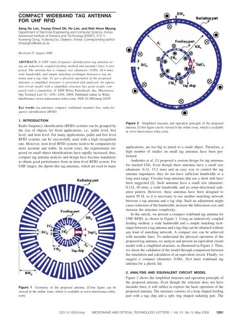
Figure 1 Geometry of the proposed <strong>antenna</strong>. [Color figure can be<br />
viewed in the online issue, which is available at www.interscience.wiley.<br />
com]<br />
Figure 2 Simplified structure and operation principle of the proposed<br />
<strong>antenna</strong>. [Color figure can be viewed in the online issue, which is available<br />
at www.interscience.wiley.com]<br />
applications, are too big to attach to a small object. There<strong>for</strong>e, a<br />
high number of studies on small <strong>tag</strong> <strong>antenna</strong>s have been per<strong>for</strong>med.<br />
Andrenko et al. [1] proposed a custom design <strong>for</strong> <strong>tag</strong> <strong>antenna</strong>s<br />
<strong>for</strong> stacked CDs. Even though these <strong>antenna</strong>s have a small size<br />
(diameter: 0.1, 33.2 mm) and an easy way to control the <strong>tag</strong><br />
<strong>antenna</strong> impedance, they do not have sufficient bandwidth or a<br />
long read range. Circular loop <strong>antenna</strong>s that use a short stub have<br />
been suggested [2]. Such <strong>antenna</strong>s have a small size (diameter:<br />
0.12, 40 mm), a wide bandwidth, and an omni-directional radiation<br />
pattern. However, these <strong>antenna</strong>s have been designed to<br />
match 50 , so it is necessary to use another matching network<br />
between a <strong>tag</strong> <strong>antenna</strong> and a <strong>tag</strong> chip. Such an adjustment might<br />
cause reduction of the bandwidth, increase the fabrication cost, and<br />
increase the structure complexity.<br />
In this article, we present a compact <strong>wideband</strong> <strong>tag</strong> <strong>antenna</strong> <strong>for</strong><br />
<strong>UHF</strong> <strong>RFID</strong>, as shown in Figure 1. Using an inductively coupled<br />
feeding method, a wide bandwidth and a simple matching technique<br />
between a <strong>tag</strong> <strong>antenna</strong> and a <strong>tag</strong> chip can be obtained without<br />
any kind of matching network. A compact size can be achieved<br />
with meander lines. To understand the physical operation of the<br />
proposed <strong>tag</strong> <strong>antenna</strong>, we analyze and present an equivalent circuit<br />
model with a simplified structure, as illustrated in Figure 2. Then,<br />
we check the validation of the model through comparison between<br />
the simulation and calculation of an equivalent circuit. Finally, we<br />
suggest a compact (diameter: 0.08, 26.4 mm) <strong>wideband</strong> <strong>tag</strong><br />
<strong>antenna</strong> <strong>for</strong> a plastic lid.<br />
2. ANALYSIS AND EQUIVALENT CIRCUIT MODEL<br />
Figure 2 shows the simplified structure and operation principle of<br />
the proposed <strong>antenna</strong>. Even though the structure does not have<br />
meander lines, it will suffice to express the basic operation of the<br />
proposed <strong>antenna</strong>. The structure consists of a loop shaped feeding<br />
part with a <strong>tag</strong> chip and a split ring shaped radiating part. The<br />
DOI 10.1002/mop MICROWAVE AND OPTICAL TECHNOLOGY LETTERS / Vol. 51, No. 5, May 2009 1291
The solution to the mutual inductance of the simplified structure is<br />
not known. There<strong>for</strong>e, we analyzed the problem and validated the<br />
results. In general, a mutual inductance can be expressed using (6),<br />
where I fp is a current on the feeding part, B fp is the magnetic flux<br />
density, which is created by I fp , and S rp is the area of the radiating<br />
part. If the feeding part, which has a radius FR s , is placed in the x-y<br />
plane, centered at the origin, and carrying a constant current I fp , the<br />
current density has only a component, as in (7). The magnetic<br />
vector potential, A, which can be derived from J, can be expressed<br />
by using a complete elliptic integral of first kind and second kind<br />
[5, 6].<br />
M 1<br />
I fps rp<br />
B fp ds rp H (6)<br />
Figure 3<br />
Equivalent circuit model of the simplified structure<br />
circumference of the radiating part should be close to /2 <strong>for</strong> the<br />
purpose of effective radiation into free space.<br />
The operation principle can be explained as follows. It is<br />
possible to assume constant current flows on the feeding part,<br />
because the feeding part is much smaller than the wavelength of<br />
<strong>UHF</strong> frequency ranges. If the current flows in a counterclockwise<br />
direction, it produces magnetic fields around the feeding loop. To<br />
cancel the magnetic fields, new magnetic fields are induced near<br />
the radiating part. There<strong>for</strong>e, a current that flows in a clockwise<br />
direction is also induced on the radiating part. It is the source to<br />
radiate into free space. The simplified structure can be expressed as<br />
an equivalent circuit model in Figure 3 [3]. The capacitance C couple<br />
between the feeding part and the radiating part is negligible,<br />
because the distance between the two parts is large. There<strong>for</strong>e,<br />
only inductive coupling survives. The input resistance and reactance<br />
of the inductively coupled feeding structure can be expressed<br />
as (1) and (2) near the resonance frequency, where M is the mutual<br />
inductance between the two parts, and R rp,o and Q rp are the<br />
radiation resistance and the quality factor of the radiating part at<br />
resonance frequency, respectively. L fp is the self inductance of the<br />
feeding part [3]. The unknown variables (L fp , M, R rp,o , and Q rp )of<br />
the equivalent circuit are analyzed and designed.<br />
R a 2fM2<br />
R rp,o<br />
1<br />
1 Q rp f/f o f o /f 2 (1)<br />
X a 2fL fp 2fM2 Q rp f/f o f o /f <br />
1 Q rp f/f o f o /f 2 (2)<br />
R rp,o<br />
The inductance of a circular loop which has radius “a” and a wire<br />
radius “b” can be calculated by (3) [4]. However, the feeding part<br />
of the simplified structure is a planar type, which has a radius FR s<br />
and width FW s , as shown in Figure 2. There<strong>for</strong>e, (3) needs to be<br />
modified. If most currents flow on the surface of the wire, from (4),<br />
the circumference of the wire is equal to the feeding part width of<br />
the simplified structure. Substituting (4) in (3), we obtain the<br />
inductance of the feeding part by (5).<br />
L loop o aln 8a<br />
<br />
b 2 (3)<br />
2b FW s 3 b FW s /2 (4)<br />
L fp o FR sln 16FR s<br />
FW s<br />
2 (5)<br />
Kk <br />
21 2<br />
1 2k 2<br />
Ek <br />
21 2<br />
1 2k 2<br />
J I fp sincos r FR s<br />
FR s<br />
(7)<br />
1 3<br />
2<br />
2 4<br />
k 4 <br />
2n 1!!<br />
<br />
2 n n!<br />
<br />
2<br />
k 2n (8)<br />
1 3 2<br />
k<br />
2 4<br />
4 <br />
2<br />
2n 1!! k<br />
<br />
2 n n!<br />
<br />
2n<br />
2n 1<br />
(9)<br />
4FR<br />
k 2 s rsin<br />
<br />
FR 2 s r 2 2FR s rsin<br />
A r, 0 4I fp FR s<br />
4FR 2 s r 2 2FR s rsin 1/ 2<br />
2 k2 Kk 2Ek<br />
k 2 <br />
(10)<br />
(11)<br />
The magnetic flux density, B, can be calculated using (12). Since<br />
the loop lies in the x-y plane (at 90°), B r becomes zero and<br />
only the B component survives. Finally, substituting (12.2) in (6),<br />
we can get the mutual inductance, M, between the feeding part and<br />
the radiating part, as shown in (13). Because the current flow<br />
direction of the feeding part is opposite to that of the radiating part,<br />
the mutual inductance has a minus sign. The radiation resistance<br />
and the reactance of a radiating part can be calculated by using<br />
ADS Momentum. The quality factor of the split ring shaped<br />
radiating part can be also calculated by using (14).<br />
M <br />
B r 1 <br />
rsin sinA (12.1)<br />
B 1 <br />
rr rA (12.2)<br />
B 0 (12.3)<br />
2 0 FR s RR 2 s<br />
k2 Kk 2Ek<br />
k<br />
<br />
2<br />
FR s 2 RR s 2 2FR s RR s 1/ 2 <br />
(13)<br />
1292 MICROWAVE AND OPTICAL TECHNOLOGY LETTERS / Vol. 51, No. 5, May 2009 DOI 10.1002/mop
Figure 4<br />
Input resistance and reactance of the simplified structure<br />
Q rp <br />
dX r<br />
2R rp,o d o<br />
<br />
o X 2 X 1<br />
(14)<br />
2R rp,o 2 1<br />
The specific dimensions were calculated to use the simplified<br />
structure in the <strong>UHF</strong> range. The results of the computation were<br />
RR s 23.8 mm, RW s 2 mm, RG s 2 mm, FR s 5.2 mm, FW s<br />
1.5 mm, TagG s 0.6 mm, and d s 17.1 mm. The unknown<br />
variables were determined to be L fp 20.6 (nH), M 2.37<br />
(nH), R rp,o 9.85 (), and Q rp 58. To confirm the validation,<br />
the input impedance of the equivalent circuit with the calculated<br />
variables was compared with the input impedance obtained from<br />
high frequency structural simulator (HFSS) simulation. Figure 4<br />
shows good agreement; hence, the availability of the inductance of<br />
the feeding part from (5) and the mutual inductance M from (13)<br />
was confirmed.<br />
3. ANTENNA DESIGN<br />
A compact <strong>wideband</strong> <strong>tag</strong> <strong>antenna</strong> with meander lines was designed<br />
and prototyped <strong>for</strong> an <strong>RFID</strong> <strong>tag</strong> chip with an input impedance of<br />
6.2-j127 () [3], as shown in Figure 5. Indeed, there are parasitic<br />
capacitances between the gaps of the meander lines. However, the<br />
basic principle of operation is nearly the same as that of the<br />
simplified structure. The design parameters of the prototype <strong>antenna</strong><br />
are RR p 8.4 mm, RW p 4.8 mm, RG p 0.5 mm, FR p<br />
2.2 mm, FW p 2 mm, FG p 0.3 mm, TagG p 1 mm, and<br />
d p 4.2 mm (refer to Fig. 1). The <strong>antenna</strong> was printed on a thin<br />
substrate of polytetrafluoroethylene ( r 3.5, tan 0.001) using<br />
copper traces ( 5.8 10 7 S/m) with a thickness of 35 m. The<br />
proposed <strong>antenna</strong> is a kind of balanced symmetric type <strong>antenna</strong>.<br />
Thus, the <strong>antenna</strong> input impedance was measured by measuring<br />
half of the <strong>antenna</strong> over a 400 400 mm 2 ground plane, as shown<br />
in Figure 6, and multiplying the measured impedance by two.<br />
Figure 7 shows the simulated return loss, which was obtained<br />
using HFSS and the measured return loss of the <strong>antenna</strong>. The<br />
simulation result at the reference level of 3 dB return loss was 102<br />
MHz (862–964 MHz), whereas the measured result at the same<br />
reference level was 102 MHz (856–958 MHz). Both results approximately<br />
cover the <strong>UHF</strong> <strong>RFID</strong> frequency bandwidth (860–960<br />
MHz). There<strong>for</strong>e, the prototype <strong>antenna</strong> can be operated continually<br />
in the <strong>UHF</strong> <strong>RFID</strong> frequency range.<br />
Figures 8 and 9 show the simulation results <strong>for</strong> the input<br />
impedance characteristic of the proposed <strong>tag</strong> <strong>antenna</strong> with a varying<br />
feeding part width, FW p , and a varying distance, d p , between<br />
the radiating and the feeding parts. Figure 8 shows the results of<br />
Figure 5 Prototype of the proposed <strong>antenna</strong> mounted on a bottle cap.<br />
[Color figure can be viewed in the online issue, which is available at<br />
www.interscience.wiley.com]<br />
varying the feeding part width FW p without changing other parameters.<br />
The feeding part width FW p controls the input reactance<br />
of the <strong>tag</strong> <strong>antenna</strong>. The reactance of the <strong>tag</strong> <strong>antenna</strong> is dependent<br />
on the <strong>tag</strong> chip due to the maximization of the power delivery to<br />
the <strong>tag</strong> <strong>antenna</strong>. The width FW p was 2 mm, which gives a complex<br />
conjugate value <strong>for</strong> the chip impedance. As the width FW p increases,<br />
the reactance of the <strong>antenna</strong> increases. There<strong>for</strong>e, it is easy<br />
to control the reactance of the <strong>tag</strong> <strong>antenna</strong>.<br />
Figure 9 shows the results when the distance d p between the<br />
radiating and the feeding parts is varied. As seen in Figure 9, the<br />
input resistance of the <strong>tag</strong> <strong>antenna</strong> is dependent on the distance d p<br />
between the radiating and feeding parts. The inductively coupled<br />
feeding method can control the input resistance of the <strong>antenna</strong> by<br />
varying the mutual coupling between the radiating and feeding<br />
Figure 6 Input impedance measurement of the proposed <strong>antenna</strong>. [Color<br />
figure can be viewed in the online issue, which is available at www.interscience.wiley.com]<br />
DOI 10.1002/mop MICROWAVE AND OPTICAL TECHNOLOGY LETTERS / Vol. 51, No. 5, May 2009 1293
Figure 7<br />
Return loss of the proposed <strong>antenna</strong><br />
Figure 9<br />
Input resistance as a function of distance between the two parts<br />
parts. The input resistance of the <strong>tag</strong> <strong>antenna</strong> increases in proportion<br />
to the squared mutual coupling in (1). As the distance d p<br />
between the parts increases, the mutual coupling decreases. As the<br />
mutual coupling decreases, the resistance of the <strong>antenna</strong> decreases.<br />
There<strong>for</strong>e, the input resistance of the <strong>tag</strong> <strong>antenna</strong> can be easily<br />
adjusted.<br />
A number of <strong>tag</strong> chips are fabricated with various impedances<br />
according to the chip providers. There<strong>for</strong>e, this method is convenient<br />
when designing <strong>tag</strong> <strong>antenna</strong>s.<br />
4. CONCLUSION<br />
In this article, to understand the physical operation of the proposed<br />
<strong>tag</strong> <strong>antenna</strong>, we have presented an analysis and an equivalent<br />
circuit model of the simplified structure. We have validated the<br />
model through a comparison between simulation and calculation<br />
of the equivalent circuit. For use in plastic lids, we have presented<br />
a compact (diameter: 0.08, 26.4 mm) <strong>wideband</strong> (102 MHz) <strong>tag</strong><br />
<strong>antenna</strong> <strong>for</strong> <strong>UHF</strong> <strong>RFID</strong>. Using an inductively coupled feeding<br />
method, a wide bandwidth and a simple matching technique can be<br />
obtained, while size reduction can also be achieved using meander<br />
lines. The prototype <strong>antenna</strong> can be operated continually in the<br />
<strong>UHF</strong> <strong>RFID</strong> frequency range.<br />
ACKNOWLEDGMENT<br />
This work was supported by KAIST BK 21(Brain Korea 21),<br />
Agency <strong>for</strong> Defense Development (ADD) through the Radiowave<br />
Detection Research Center (RDRC) at KAIST, and the Samsung<br />
Advanced Institute of Technology (SAIT).<br />
REFERENCES<br />
1. A.S. Andrenko, M. Kai, T. Maniwa, and T. Yamagajo, <strong>Compact</strong> printed<br />
on CD <strong>UHF</strong> <strong>RFID</strong> <strong>tag</strong> <strong>antenna</strong>s, IEEE Antennas and Propagation<br />
Society International Symposium, 2007, Honolulu, HI, pp. 5455–5458.<br />
2. H.-K. Ryu and J.-M. Woo, Miniaturisation of circular loop <strong>antenna</strong><br />
using short stub <strong>for</strong> <strong>RFID</strong> system, Electron Lett 42 (2006), 955–956.<br />
3. H.W. Son and C.S. Pyo, Design of <strong>RFID</strong> <strong>tag</strong> <strong>antenna</strong>s using an inductively<br />
coupled feed, Electron Lett 41 (2005), 994–996.<br />
4. C.A. Balanis, Antenna theory, 3rd ed., <strong>Wiley</strong> Interscience, Hoboken,<br />
NJ, 2005.<br />
5. J.D. Jackson, Classical electrodynamics, <strong>Wiley</strong>, New York, NY, 1998.<br />
6. I.S. Gradshteyn and I.M. Ryzhik, Table of integrals, series, and products,<br />
Academic press, Orlando, FL, 1980.<br />
© 2009 <strong>Wiley</strong> Periodicals, Inc.<br />
CASCADED DUAL-MODE SQUARE-<br />
LOOP RESONATORS USING HILBERT-<br />
CURVE PERTURBATION FOR WIDE<br />
BANDPASS FILTER APPLICATIONS<br />
Ji-Chyun Liu, 1 Chiung-Hung Li, 1 Ching-Pin Kuei, 2 and<br />
Bing-Hao Zeng 3<br />
1 Department of Electrical Engineering, Ching Yun University, Chung-<br />
Li, Tao-yuan 32097, Taiwan, Republic of China; Corresponding<br />
author: jichyun@cyu.edu.tw<br />
2 Department of Electronics Engineering, Ching Yun University,<br />
Chung-Li, Tao-yuan 32097, Taiwan, Republic of China<br />
3 Department of Communication Engineering, Yuan Ze University,<br />
Chung-Li, Tao-yuan 32003, Taiwan, Republic of China<br />
Received 26 August 2008<br />
Figure 8<br />
Input reactance as a function of feeding part width<br />
ABSTRACT: The cascaded dual-mode square-loop resonator<br />
(DMSLR) with Hilbert-curve perturbation is introduced to design<br />
wide band-pass filter in this article. To obtain low insertion loss<br />
(0.85 dB), high out-of-band rejection level (51.82 dB), and wider<br />
band (BW 62.3%) responses, using Hilbert-curve perturbation and<br />
1294 MICROWAVE AND OPTICAL TECHNOLOGY LETTERS / Vol. 51, No. 5, May 2009 DOI 10.1002/mop