Reliable Circuit Techniques for Low-Voltage Analog Design in Deep ...
Reliable Circuit Techniques for Low-Voltage Analog Design in Deep ...
Reliable Circuit Techniques for Low-Voltage Analog Design in Deep ...

You also want an ePaper? Increase the reach of your titles
YUMPU automatically turns print PDFs into web optimized ePapers that Google loves.
30 Fayomi, Sawan and Roberts<br />
2.2. <strong>Analog</strong> CMOS Switches<br />
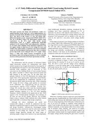
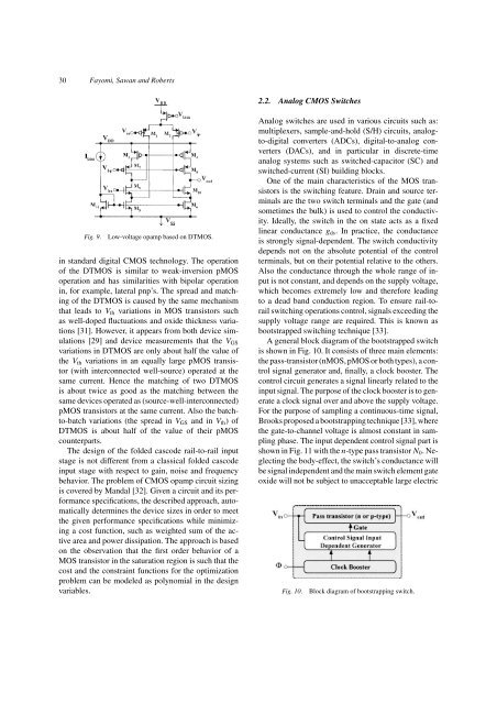
Fig. 9.<br />
<strong>Low</strong>-voltage opamp based on DTMOS.<br />
<strong>in</strong> standard digital CMOS technology. The operation<br />
of the DTMOS is similar to weak-<strong>in</strong>version pMOS<br />
operation and has similarities with bipolar operation<br />
<strong>in</strong>, <strong>for</strong> example, lateral pnp’s. The spread and match<strong>in</strong>g<br />
of the DTMOS is caused by the same mechanism<br />
that leads to V th variations <strong>in</strong> MOS transistors such<br />
as well-doped fluctuations and oxide thickness variations<br />
[31]. However, it appears from both device simulations<br />
[29] and device measurements that the V GS<br />
variations <strong>in</strong> DTMOS are only about half the value of<br />
the V th variations <strong>in</strong> an equally large pMOS transistor<br />
(with <strong>in</strong>terconnected well-source) operated at the<br />
same current. Hence the match<strong>in</strong>g of two DTMOS<br />
is about twice as good as the match<strong>in</strong>g between the<br />
same devices operated as (source-well-<strong>in</strong>terconnected)<br />
pMOS transistors at the same current. Also the batchto-batch<br />
variations (the spread <strong>in</strong> V GS and <strong>in</strong> V th )of<br />
DTMOS is about half of the value of their pMOS<br />
counterparts.<br />
The design of the folded cascode rail-to-rail <strong>in</strong>put<br />
stage is not different from a classical folded cascode<br />
<strong>in</strong>put stage with respect to ga<strong>in</strong>, noise and frequency<br />
behavior. The problem of CMOS opamp circuit siz<strong>in</strong>g<br />
is covered by Mandal [32]. Given a circuit and its per<strong>for</strong>mance<br />
specifications, the described approach, automatically<br />
determ<strong>in</strong>es the device sizes <strong>in</strong> order to meet<br />
the given per<strong>for</strong>mance specifications while m<strong>in</strong>imiz<strong>in</strong>g<br />
a cost function, such as weighted sum of the active<br />
area and power dissipation. The approach is based<br />
on the observation that the first order behavior of a<br />
MOS transistor <strong>in</strong> the saturation region is such that the<br />
cost and the constra<strong>in</strong>t functions <strong>for</strong> the optimization<br />
problem can be modeled as polynomial <strong>in</strong> the design<br />
variables.<br />
<strong>Analog</strong> switches are used <strong>in</strong> various circuits such as:<br />
multiplexers, sample-and-hold (S/H) circuits, analogto-digital<br />
converters (ADCs), digital-to-analog converters<br />
(DACs), and <strong>in</strong> particular <strong>in</strong> discrete-time<br />
analog systems such as switched-capacitor (SC) and<br />
switched-current (SI) build<strong>in</strong>g blocks.<br />
One of the ma<strong>in</strong> characteristics of the MOS transistors<br />
is the switch<strong>in</strong>g feature. Dra<strong>in</strong> and source term<strong>in</strong>als<br />
are the two switch term<strong>in</strong>als and the gate (and<br />
sometimes the bulk) is used to control the conductivity.<br />
Ideally, the switch <strong>in</strong> the on state acts as a fixed<br />
l<strong>in</strong>ear conductance g ds .Inpractice, the conductance<br />
is strongly signal-dependent. The switch conductivity<br />
depends not on the absolute potential of the control<br />
term<strong>in</strong>als, but on their potential relative to the others.<br />
Also the conductance through the whole range of <strong>in</strong>put<br />
is not constant, and depends on the supply voltage,<br />
which becomes extremely low and there<strong>for</strong>e lead<strong>in</strong>g<br />
to a dead band conduction region. To ensure rail-torail<br />
switch<strong>in</strong>g operations control, signals exceed<strong>in</strong>g the<br />
supply voltage range are required. This is known as<br />
bootstrapped switch<strong>in</strong>g technique [33].<br />
A general block diagram of the bootstrapped switch<br />
is shown <strong>in</strong> Fig. 10. It consists of three ma<strong>in</strong> elements:<br />
the pass-transistor (nMOS, pMOS or both types), a control<br />
signal generator and, f<strong>in</strong>ally, a clock booster. The<br />
control circuit generates a signal l<strong>in</strong>early related to the<br />
<strong>in</strong>put signal. The purpose of the clock booster is to generate<br />
a clock signal over and above the supply voltage.<br />
For the purpose of sampl<strong>in</strong>g a cont<strong>in</strong>uous-time signal,<br />
Brooks proposed a bootstrapp<strong>in</strong>g technique [33], where<br />
the gate-to-channel voltage is almost constant <strong>in</strong> sampl<strong>in</strong>g<br />
phase. The <strong>in</strong>put dependent control signal part is<br />
shown <strong>in</strong> Fig. 11 with the n-type pass transistor N 0 . Neglect<strong>in</strong>g<br />
the body-effect, the switch’s conductance will<br />
be signal <strong>in</strong>dependent and the ma<strong>in</strong> switch element gate<br />
oxide will not be subject to unacceptable large electric<br />
Fig. 10.<br />
Block diagram of bootstrapp<strong>in</strong>g switch.