Reliable Circuit Techniques for Low-Voltage Analog Design in Deep ...
Reliable Circuit Techniques for Low-Voltage Analog Design in Deep ...
Reliable Circuit Techniques for Low-Voltage Analog Design in Deep ...

Create successful ePaper yourself
Turn your PDF publications into a flip-book with our unique Google optimized e-Paper software.
22 Fayomi, Sawan and Roberts<br />
2.1. <strong>Low</strong>-<strong>Voltage</strong> Operational Amplifier<br />
One of the most important basic build<strong>in</strong>g blocks <strong>in</strong><br />
analog and mixed-mode circuits is the operational<br />
amplifier. In a low-voltage (LV) opamp, the m<strong>in</strong>imum<br />
supply value is imposed by the differential pair of the<br />
<strong>in</strong>put stage and is equal to the threshold voltage (V th )<br />
plus two overdrive voltages (V DSat ). In typical CMOS<br />
processes, this value turns out to be around 1-V. On<br />
the other hand, the ma<strong>in</strong> limitation of differential pairs<br />
is the reduced <strong>in</strong>put common-mode range (ICMR). In<br />
order to m<strong>in</strong>imize the supply requirements of the <strong>in</strong>put<br />
stage, both <strong>in</strong>put term<strong>in</strong>als of an opamp must work<br />
with potentials very close to one of the supply rails. To<br />
overcome this limitation, several schemes <strong>for</strong> discretetime<br />
(switched) operation with a s<strong>in</strong>gle supply down to<br />
1Vand large output signal sw<strong>in</strong>gs have been recently<br />
reported [2–10]. The switched-opamp (SO) technique<br />
[2] has been shown to be a promis<strong>in</strong>g low-cost solution<br />
to realize switched-capacitor (SC) circuits <strong>in</strong> standard<br />
CMOS processes. The SO elim<strong>in</strong>ates critical MOS<br />
switches that set the m<strong>in</strong>imum supply voltage to allow<br />
sub-1-V operation of the SC circuits [4] and, thus,<br />
does not have a reliability problem. S<strong>in</strong>ce then, a few<br />
modifications have been proposed to improve the per<strong>for</strong>mance<br />
of the SO techniques <strong>in</strong> terms of operation<br />
speed and compatibility with exist<strong>in</strong>g SC circuits.<br />
In switched applications, no <strong>in</strong>put sw<strong>in</strong>g is required<br />
<strong>for</strong> the opamp s<strong>in</strong>ce both <strong>in</strong>put term<strong>in</strong>als operate at<br />
one of the supply rails. Many others 1 V opamps<br />
are cont<strong>in</strong>uous-time <strong>for</strong> differential operation but use<br />
switches <strong>for</strong> the common-mode. Those techniques will<br />
not be covered <strong>in</strong> this paper. Most of cont<strong>in</strong>uous-time<br />
techniques will be addressed and can be classified <strong>in</strong><br />
three categories. The first technique is mostly based<br />
on level shift<strong>in</strong>g of the common <strong>in</strong>put signal to a<br />
value capable of driv<strong>in</strong>g the <strong>in</strong>put term<strong>in</strong>als [11–18].<br />
Cont<strong>in</strong>uous-time and switched-capacitor techniques<br />
have been developed to shift the <strong>in</strong>put. The second<br />
concept makes use of the bulk-driven MOS transistor<br />
[19, 20] and current driven bulk [21] techniques, while<br />
the local charge pump based approach is described <strong>in</strong><br />
[22]. The latter technique will not be addressed s<strong>in</strong>ce it<br />
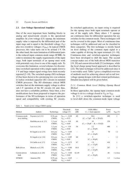
is not widely used. Table 1 gives a simplified overview<br />
of methods used <strong>for</strong> achiev<strong>in</strong>g almost rail-to-rail lowvoltage<br />
opamp designs with their related per<strong>for</strong>mance.<br />
Detailed description will be given below.<br />
2.1.1. Common Mode Level Shift<strong>in</strong>g Opamp Based<br />
Method<br />
In these approaches, the opamp <strong>in</strong>put common-mode<br />
voltage is set to a voltage closed to V SS or V DD .<br />
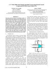
In [11] a switched-capacitor technique is used<br />
to level-shift down the common-mode <strong>in</strong>put voltage<br />
Table 1.<br />
Trends <strong>in</strong> low-voltage CMOS opamp.<br />
Threshold Ga<strong>in</strong> UGB (MHz) Power<br />
Method Authors Technology voltage (V) (dB) C 1 = load capacitor (µW) V DD (V)<br />
Common-mode Fayomi et al. [11] 0.18-µm V th,p =−0.48 60 26.6 400 1<br />
level shift<strong>in</strong>g CMOS V th,n = 0.52 (C 1 = 5pF− R 1 = 20 k)<br />
Karthikeyan et al. [13] 1.2-µm V th,p =−0.8 60 10 150 1<br />
CMOS V th,n = 0.60 (C 1 = 20 pF − R 1 = 10 k)<br />
Lee et al. [14] 1.2-µm V th,p =−0.8 58 2.2 400 1<br />
CMOS V th,n = 0.60 (C 1 = 20 pF)<br />
R-Angulo et al. [15] 0.8-µm V th,p ≈−0.85 – 13 70 1.2<br />
CMOS V th,n ≈ 0.85 (C 1 = 10 pF)<br />
R-Angulo et al. [16] 0.8-µm V th,p ≈−0.85 60 5 – 1.2<br />
CMOS V th,n ≈ 0.85 (C 1 = 50 pF)<br />
D-Carillo et al. [17] 1.2-µm V th,p ≈−0.75 87 1.9 410 1<br />
CMOS V th,n ≈ 0.75 (C 1 = 15 pF)<br />
Bulk-driven Blalock et al. [19] 2.0-µm V th,p ≈−0.80 44.8 1.3 287 1<br />
CMOS V th,n ≈ 0.80 (C 1 = 22 pF)<br />
Current driven Lehmann et al. [20] 0.5-µm V th,p ≈−0.60 62–69 2 40 1 or less<br />
bulk CMOS V th,n ≈ 0.60 (C 1 = 20 pF)<br />
DTMOS Annema [29] 0.35-µm V th,p =−0.65 – – 1.2 1 or less<br />
CMOS V th,n = 0.65