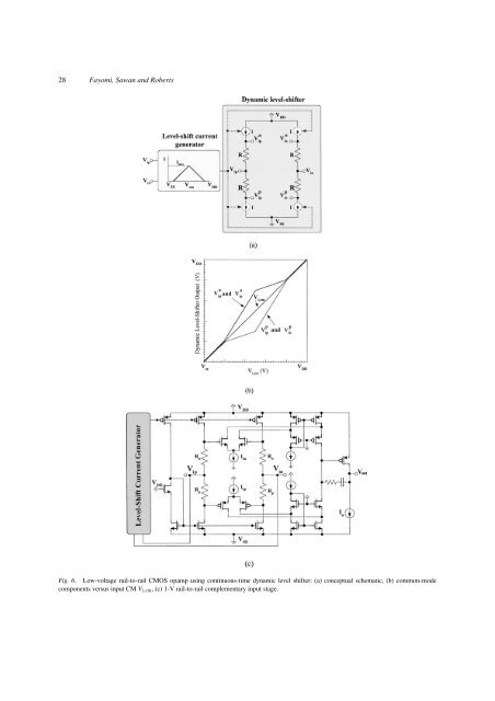
28 Fayomi, Sawan and Roberts Fig. 6. <strong>Low</strong>-voltage rail-to-rail CMOS opamp us<strong>in</strong>g cont<strong>in</strong>uous-time dynamic level shifter: (a) conceptual schematic, (b) common-mode components versus <strong>in</strong>put CM V i,cm , (c) 1-V rail-to-rail complementary <strong>in</strong>put stage.
<strong>Reliable</strong> <strong>Circuit</strong> <strong>Techniques</strong> <strong>for</strong> <strong>Low</strong>-<strong>Voltage</strong> <strong>Analog</strong> <strong>Design</strong> 29 2.1.2. Bulk Driven and Current Driven Bulk MOSFET Based Opamp Method <strong>Low</strong>-voltage rail-to-rail CM <strong>in</strong>put sw<strong>in</strong>g can also be achieved us<strong>in</strong>g the bulk-driven differential pair technique. The orig<strong>in</strong>al purpose of this technique was to yield a small g m and to improve l<strong>in</strong>earity [19]. In [20], a 1-V opamp was designed us<strong>in</strong>g the depletion characteristic of the bulk-driven transistors to have a railto-rail CM range and to meet the low-voltage requirement. The full opamp circuit implementation is shown <strong>in</strong> Fig. 7. This type of opamp requires low supply, about (V GS +V SD,sat ). Its shortcom<strong>in</strong>g is that the transconductance value changes dramatically (about 2 times) with the CM <strong>in</strong>put voltage. The equivalent <strong>in</strong>put referred noise of a bulk-driven MOS amplifier is larger than the conventional gate-driven MOS amplifier because of its small transconductance. It has the prone turn on the parasitic bipolar transistors, which may result <strong>in</strong> a latch-up problem. The threshold voltage of a MOS transistor as a function of bulk-source voltage V BS is given by Eq. (9): V th = V th0 + γ (√ |2 · φ F − V BS |− √ |2 · φ F | ) (9) where V th0 is zero bias threshold voltage, γ the bulk effect factor and φ F the Fermi potential. For a p- channel transistor, 2·φ F ≈−0.7V,γ ≈−0.5 √ V and V th0 ≈−0.6 V,typically, and a bulk bias V BS is normally greater than 0, which leads to an <strong>in</strong>crease of the threshold voltage. However, by bias<strong>in</strong>g V BS < 0V,we can actually decrease the threshold voltage [28]. Thus, to reduce the threshold voltage as much as possible, the device is bulk biased as high as possible. This will, however, <strong>for</strong>ward bias the bulk-source diode, i.e., the base-emitter diode of the associated parasitic bipolar transistor, thereby turn<strong>in</strong>g on this BJT. |V BS | is limited Fig. 7. 1-V rail-to-rail bulk driven CMOS opamp. Fig. 8. 1-V CDB folded cascode OTA. by how much current the new BJT can tolerate. This is the basic idea of the current driven bulk (CDB) circuit technique. This method has been used to implement a 1-V CMOS OTA [21] as shown <strong>in</strong> Fig. 8. The threshold voltage of the differential pair (M 1 –M 2 )isreduced and thus leads to a direct improvement of the CM <strong>in</strong>put range. Note that, only one current source has been used <strong>for</strong> the common bulk term<strong>in</strong>al <strong>in</strong> the pair (rather than <strong>in</strong>dividual current drives <strong>for</strong> each transistor); otherwise, mismatch problems <strong>in</strong> the pair will appear. Any noise <strong>in</strong>jected because of the current drive will enter the amplifier as a common-mode signal and thus will be rejected. Operation of this circuit down to 0.7 V has been reported. Current driv<strong>in</strong>g the bulk <strong>in</strong>troduces unsuited effects <strong>in</strong> the result<strong>in</strong>g devices. The first obvious one is the parallel connection of the BJT emitter/collector with the MOS source/dra<strong>in</strong>; this must lower the device output impedance. If the BJT emitter current is much smaller than the MOS source current, the effect is negligible. Noise from the BJT would also enter the circuit, butaga<strong>in</strong>, if the current <strong>in</strong> this device is low, we would expect only a small amount of added noise. It’s evident that the dra<strong>in</strong>-bulk capacitance has a major impact on high frequency circuit per<strong>for</strong>mance. Several ways can be used to cancel its effect. A similar technique has been used by Annema [29] to build an opamp <strong>for</strong> low-voltage bandgap reference voltage circuit (Fig. 9). A dynamic threshold MOS (DTMOS) transistor [30] is used <strong>in</strong>stead. The <strong>in</strong>put driven differential pair consists of DTMOS M 1 –M 2 . The device is basically a MOS transistor with an <strong>in</strong>terconnected well and gate. Only p-type DTMOS can be used due to the fact that their n-well can be controlled