Reliable Circuit Techniques for Low-Voltage Analog Design in Deep ...
Reliable Circuit Techniques for Low-Voltage Analog Design in Deep ...
Reliable Circuit Techniques for Low-Voltage Analog Design in Deep ...

Create successful ePaper yourself
Turn your PDF publications into a flip-book with our unique Google optimized e-Paper software.
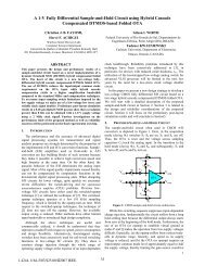
24 Fayomi, Sawan and Roberts<br />
fully differential <strong>in</strong>vert<strong>in</strong>g opamp configuration <strong>in</strong>to a<br />
low-voltage design. In this case, two current sources or<br />
two resistors are required to connect to the fully differential<br />
opamp <strong>in</strong>puts, and the values of the current<br />
sources or resistors can be determ<strong>in</strong>ed based on the<br />
<strong>in</strong>put and output common-mode voltages. Add<strong>in</strong>g the<br />
current source or resistor <strong>in</strong>duces m<strong>in</strong>imal effects on<br />
the low frequency response s<strong>in</strong>ce they are connected to<br />
the virtual ground of the opamp. However, at high frequency,<br />
the bandwidths of the two schemes are different.<br />
The obta<strong>in</strong>ed reduction <strong>in</strong> supply voltage, however,<br />
comes with a price of <strong>in</strong>creas<strong>in</strong>g the overall noise. The<br />
mean squared output noise Vno 2 <strong>for</strong> both circuits shown<br />
<strong>in</strong> Fig. 3 can be written as:<br />
vno 2 = ( (<br />
Inl 2 + I nf 2 + I n 2 )<br />
R<br />
2<br />
f + vna<br />
2 1 + R ) 2<br />
f<br />
(6)<br />
R 1 //R x<br />
Fig. 2.<br />
Level Shifter transfer function.<br />
hence the m<strong>in</strong>imum supply voltage of the circuit is<br />
V DS,sat + 2V SD,sat +|V th,p |.Ifthe <strong>in</strong>put stage of the<br />
opamp is realized us<strong>in</strong>g nMOS differential pair, sett<strong>in</strong>g<br />
v x close to V DD with a pMOS current source I B connected<br />
between the opamp negative <strong>in</strong>put term<strong>in</strong>al and<br />
V DD will m<strong>in</strong>imize the supply voltage. A resistor or a<br />
MOSFET operat<strong>in</strong>g <strong>in</strong> the triode region can be used to<br />
bias the opamp <strong>in</strong>put common-mode voltage as shown<br />
<strong>in</strong> Fig. 3(b). The resistance R B can be determ<strong>in</strong>ed as:<br />
R B =<br />
v x<br />
V DD<br />
2<br />
− v x<br />
(R 1 //R f ) (5)<br />
The second approach has the advantage of sett<strong>in</strong>g<br />
v x to a value lower than one V DS,sat (but greater than<br />
the ground). The method can be extended to convert a<br />
where I nl , I nf and V na are the equivalent noise currents<br />
of R 1 , R f and the equivalent noise voltage of the opamp<br />
respectively. When compared to the case without the<br />
addition of R B and I B , additional terms In 2 and R x are<br />
presented <strong>in</strong> (6). For Fig. 3(a), R x is equivalent to r ds ,<br />
and In 2 is due to the noise current of I B.With v x =<br />
V DS,sat , In 2 can then be derived us<strong>in</strong>g (4) as<br />
In 2 = 16 V DD<br />
3 kT − v<br />
2 x<br />
v x (R f //R 1 )<br />
(7)<br />
where only thermal noise is considered. For Fig. 3(b),<br />
R x is equal to R B , and In 2 is due to the equivalent noise<br />
current of R B that can be also described us<strong>in</strong>g (7) except<br />
that the scal<strong>in</strong>g factor 16/3 is now equal 4. In<br />
most cases, the term due to the opamp noise V 2<br />
na is<br />
usually the dom<strong>in</strong>ant factor. S<strong>in</strong>ce R B < R 1 < r ds , the<br />
circuit shown <strong>in</strong> Fig. 3(a) has lower noise than the circuit<br />
shown <strong>in</strong> Fig. 3(b). Furthermore, due to the term<br />
In 2 ,ithas a slightly higher noise than the case when<br />
Fig. 3.<br />
Bias<strong>in</strong>g schemes <strong>for</strong> low-voltage CMOS opamp <strong>in</strong> a s<strong>in</strong>gle-ended configuration us<strong>in</strong>g: (a) a current source and (b) a resistor.