IL410 datasheet - Datasheet Catalog
IL410 datasheet - Datasheet Catalog
IL410 datasheet - Datasheet Catalog

Create successful ePaper yourself
Turn your PDF publications into a flip-book with our unique Google optimized e-Paper software.
This document was created with FrameMaker 4.0.4<br />
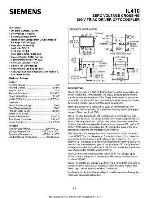
<strong>IL410</strong><br />
ZERO VOLTAGE CROSSING<br />
600 V TRIAC DRIVER OPTOCOUPLER<br />
FEATURES<br />
• On-State Current, 300 mA<br />
• Zero Voltage Crossing<br />
• Blocking Voltage, 600 V<br />
• Isolation Test Voltage from Double Molded<br />
Package, 5300 VAC RMS<br />
• High Input Sensitivity<br />
I FT =2 mA, PF=1.0<br />
I FT =5 mA, PF≤1.0<br />
• High Static dv/dt 10,000 V/µs<br />
• Inverse Parallel SCRs Provide<br />
Commutating dv/dt >10K V/µs<br />
• Very Low Leakage
Characteristics<br />
Symbol Min Typ Max Unit Condition<br />
Emitter<br />
Forward Voltage V F 1.16 1.35 V I F =10 mA<br />
Reverse Current I R 0.1 10 µA V R =6 V<br />
Capacitance C O 25 pF V F =0 V, f=1 MHz<br />
Thermal Resistance, Junction to Lead R THJL 750 °C/W<br />
Output Detector<br />
Off-State Voltage V D(RMS) 424 460 V I D(RMS) =70 mA<br />
Off-State Current I D(RMS)1 10 100 µA V D =600 V, T A =100°C, I F =0 mA<br />
Off State Current I D(RMS)2 200 µA V D =600 V, I F =Rated I FT<br />
On-State Voltage V TM 1.7 3 V I T =300 mA<br />
On State Current I TM 300 mA PF=1.0, V T(RMS) =1.7 V<br />
Surge (Non-Repititive),<br />
On-State Current I TSM 3 A f=50 Hz<br />
Trigger Current 1 I FT1 2.0 mA V D =5 V<br />
Trigger Current 2 I FT2 6.0 mA V OP =220 V, f=50 Hz, T j =100°C, t pF >10 ms<br />
Trigger Current Temp. Gradient ∆I FT1 /∆T j<br />
∆I FT2 /∆T j<br />
7<br />
7<br />
14<br />
14<br />
µA/K<br />
µA/K<br />
Inhibit Voltage Temp. Gradient ∆V DINH /∆T j -20 mV/K<br />
Off-State Current in Inhibit State I DINH 50 200 µA I F =I FT1 , V DRM<br />
Capacitance Between Input and<br />
Output Circuit<br />
C IO 2.0 pF V D =0, f=1 kHz<br />
Holding Current I H 65 500 µA<br />
Latching Current I L 5 mA V T =2.2 V<br />
Zero Cross Inhibit Voltage V IH 15 25 V I F =Rated I FT<br />
Turn-On Time t ON 35 µs V RM =V DM =424 VAC<br />
Turn-Off Time t OFF 50 µs PF=1.0, I T =300 mA<br />
Critical Rate of Rise of Off-State<br />
Voltage<br />
Critical Rate of Rise of Voltage<br />
at Current Commutation<br />
Critical Rate of Rise of On-State<br />
Current<br />
Thermal Resistance,<br />
Junction to Lead<br />
Insulation and Isolation<br />
Critical Rate of Rise of Coupled<br />
Input/Output Voltage<br />
dv/dt cr 10000<br />
dv/dt cr 5000<br />
dv/dt crq 10000<br />
dv/dt crq 5000<br />
V/µs<br />
V/µs<br />
V/µs<br />
V/µs<br />
di/dt cr 8 A/ms<br />
R THJL 150 °C/W<br />
VD=0.67 V DRM , T j =25°C<br />
T j =80°C<br />
V D =0.67 V DRM , di/dt crq ≤ 15 A/ms<br />
T j =25°C<br />
T j =80°C<br />
dv (IO) /dt 10000 V/µs I T =0 A, V RM =V DM =424 VAC<br />
Common Mode Coupling Capacitor C CM 0.01 pF<br />
Packing Capacitance C IO 0.8 pF f=1 MHz, V IO =0 V<br />
Isolation Test Voltag, Input-Output V ISO 5300 VAC RMS Relative Humidity ≤ 50%<br />
Creepage ≥7 mm<br />
Clearance ≥7 mm<br />
Creepage Tracking Resistance per DIN<br />
IEC 112/VDE 0303, Part 1 Group IIIa<br />
per DIN VDE 10110<br />
CTI 175<br />
Isolation Resistance<br />
R is<br />
≥10 12<br />
R is ≥10 11<br />
Ω<br />
Ω<br />
V IO =500 V T A =25°C<br />
T A +100°C<br />
5–2<br />
<strong>IL410</strong>
Power Factor Considerations<br />
A snubber isn’t needed to eliminate false operation of the<br />
TRIAC driver because of the <strong>IL410</strong>’s high static and commutating<br />
dv/dt with loads between 1 and 0.8 power factors.<br />
When inductive loads with power factors less than 0.8 are<br />
being driven, include a RC snubber or a single capacitor<br />
directly across the device to damp the peak commutating<br />
dv/dt spike. Normally a commutating dv/dt causes a turningoff<br />
device to stay on due to the stored energy remaining in<br />
the turning-off device.<br />
But in the case of a zero voltage crossing optotriac, the<br />
commutating dv/dt spikes can inhibit one half of the TRIAC<br />
from turning on. If the spike potential exceeds the inhibit<br />
voltage of the zero cross detection circuit, half of the TRIAC<br />
will be held-off and not turn-on. This hold-off condition can<br />
be eliminated by using a snubber or capacitor placed<br />
directly across the optotriac as shown in Figure 1. Note that<br />
the value of the capacitor increases as a function of the load<br />
current.<br />
Figure 1. Shunt capacitance versus load current<br />
1<br />
Cs(µF)= 0.0032(µF)* 10^(0.0066IL(mA))<br />
Cs - Shunt Capacitance - µF<br />
.1<br />
.01<br />
.001<br />
0<br />
50<br />
Ta = 25°C, PF = 0.3<br />
IF = 2.0mA<br />
100 150 200 250 300<br />
IL - Load Current - mA(RMS)<br />
350<br />
400<br />
The hold-off condition also can be eliminated by providing a<br />
higher level of LED drive current. The higher LED drive provides<br />
a larger photocurrent which causes the phototransistor<br />
to turn-on before the commutating spike has activated<br />
the zero cross network. Figure 2 shows the relationship of<br />
the LED drive for power factors of less than 1.0. The curve<br />
shows that if a device requires 1.5 mA for a resistive load,<br />
then 1.8 times (2.7 mA) that amount would be required to<br />
control an inductive load whose power factor is less than<br />
0.3.<br />
Figure 2. Normalized LED trigger current versus<br />
power factor<br />
NIFth - Normalized LED<br />
Trigger Current<br />
2.0<br />
1.8<br />
1.6<br />
1.4<br />
1.2<br />
1.0<br />
0.8<br />
0.0<br />
0.2<br />
IFth Normalized to IFth @ PF = 1.0<br />
Ta = 25°C<br />
0.4 0.6 0.8<br />
PF - Power Factor<br />
1.0<br />
Figure 3. Forward voltage versus forward current<br />
VF - Forward Voltage - V<br />
1.4<br />
1.3<br />
1.2<br />
1.1<br />
1.0<br />
0.9<br />
0.8<br />
0.7<br />
.1<br />
1<br />
10<br />
IF - Forward Current - mA<br />
Figure 4. Peak LED current versus duty factor, Tau<br />
If(pk) - Peak LED Current - mA<br />
10000<br />
1000<br />
100<br />
Duty Factor<br />
.005<br />
.01<br />
.02<br />
.05<br />
.1<br />
.2<br />
.5<br />
Ta = -55°C<br />
Ta = 25°C<br />
Ta = 85°C<br />
τ<br />
t<br />
τ<br />
DF = /t<br />
100<br />
1.2<br />
10<br />
10 -6 10 -5 10 -4 10 -3 10 -2 10 -1 10 0 10 1<br />
t - LED Pulse Duration - s<br />
5–3<br />
<strong>IL410</strong>
Figure 5. Maximum LED power dissipation<br />
P LED - LED Power - mW<br />
150<br />
100<br />
50<br />
Figure 8. Current reduction<br />
I TRMS =f(T PIN5 ), R thJ–PIN5 =16.5 K/W<br />
Thermocouple measurement must be performed<br />
potentially separated to A1 and A2. Measuring<br />
junction as near as possible at the case.<br />
0<br />
-60<br />
-40<br />
-20<br />
0<br />
20<br />
40<br />
60<br />
80<br />
100<br />
Ta - Ambient Temperature - °C<br />
Figure 6. Typical output characteristics<br />
I T = f(V T ), parameter: T j<br />
Figure 9. Typical trigger delay time<br />
t gd =f (I F I FT25∞C ), V D =200 V, f=40 to 60 Hz,<br />
parameter: T j<br />
Figure 7. Current reduction<br />
I TRMS =f(T A ), R thJA =125 K/W<br />
Device switch soldered in pcb or base plate.<br />
Figure 10. Typical inhibit current<br />
I DINH =f(I F /I FT25∞C )<br />
V D =600 V, parameter: T j<br />
5–4<br />
<strong>IL410</strong>
Figure 11. Power dissipation40 to 60 Hz<br />
line operation, P TOT =f(I TRMS )<br />
Current commutation:<br />
The values 100 A/ms with following peak reverse recovery current >80 mA should<br />
not be exceeded.<br />
Avoiding high-frequency turn-off current oscillations:<br />
This effect can occur when switching a circuit. Current oscillations which appear<br />
essentially with inductive loads of a higher winding capacity result in current commutation<br />
and can generate a relatively high peak reverse recovery current. The following<br />
alternating protective measures are recommended for the individual<br />
operating states:<br />
1—Apply a capacitor to the supply pins at the load-side.<br />
1<br />
6<br />
2<br />
5<br />
0.1 µF 220 V~<br />
3<br />
4<br />
Figure 12. Typical static inhibit voltage<br />
limit<br />
V DINHmin = f(I F /I FT 25°C), parameter: T j<br />
Device zero voltage switch can be triggered<br />
only in hatched area below T j curves.<br />
2— Connect a series resistor to the <strong>IL410</strong> output and bridge both by a<br />
capacitor.<br />
33 Ω<br />
1 6<br />
2<br />
5<br />
22 nF 220 V~<br />
3<br />
4<br />
3—Connect a choke of low winding capacity in series, e.g., a<br />
ringcore choke, with higher load currents.<br />
500 µH<br />
1<br />
6<br />
2<br />
5<br />
22 nF 220 V~<br />
3<br />
4<br />
Note:<br />
Measures 2 to 3 are especially required for the load separated from the <strong>IL410</strong> during operation.<br />
The above mentioned effects do not occur with <strong>IL410</strong> circuits which are connected to<br />
the line by transformers and which are not mechanically interrupted.<br />
In such cases as well as in applications with a resistive load the corresponding protective<br />
circuits can be neglected.<br />
5–5<br />
<strong>IL410</strong>
Technical Information<br />
Commutating Behavior<br />
The use of a triac at the output creates difficulties in commutation<br />
due to both the built-in coupled thyristor systems.<br />
The triac can remain conducting by parasitic triggering after<br />
turning off the control current. However, if the <strong>IL410</strong> is<br />
equipped with two separate thyristor chips featuring high dv/<br />
dt strength, no RC circuit is needed in case of commutation.<br />
Control And Turn-On Behavior<br />
The trigger current of the <strong>IL410</strong> has a positive temperature<br />
gradient. The time which expires from applying the control<br />
current to the turn-on of the load current is defined as the trigger<br />
delay time (tgd). On the whole this is a function of the<br />
overdrive meaning the ratio of the applied control current versus<br />
the trigger current (I F /I FT ). If the value of the control current<br />
corresponds to that of the individual trigger current of<br />
<strong>IL410</strong> turn-on delay times amounts to a few milliseconds only.<br />
The shortest times of 5 to 10 µs can be achieved for an overdrive<br />
greater or equal than 10. The trigger delay time rises<br />
with an increase in temperature.<br />
For very short control current pulses (t plF
This <strong>datasheet</strong> has been download from:<br />
www.<strong>datasheet</strong>catalog.com<br />
<strong>Datasheet</strong>s for electronics components.